


On July 1, 2026, China’s Ministry of Commerce issued Announcement No. 26 of 2026, further improving the reporting and handling mechanisms for violations of export controls on critical strategic minerals such as gallium, germanium, and indium. This marks a notable tightening of enforcement since China introduced export licensing requirements for gallium and germanium in August 2023.

China’s 15th Five-Year Plan Outline
In the section on “Fostering and Developing New Industries and Emerging Tracks” of China’s 15th Five-Year Plan Outline, ultra-wide-bandgap semiconductors such as gallium oxide and diamond are included in the national strategic development agenda for the first time.

Hubei Province’s 15th Five-Year Plan Outline
Hubei Province’s 15th Five-Year Plan Outline incorporates “advanced compound semiconductor materials” into its development strategy, specifically highlighting gallium nitride (GaN), gallium oxide (Ga₂O₃), and diamond, while emphasizing the simultaneous advancement of technological innovation and technology commercialization.
In March 2026, Jiufengshan Laboratory validated a Ga₂O₃ device with a breakdown voltage exceeding 9,000 V. In June, Hangzhou Gallium Ren Semiconductor announced the completion of the world’s first 6-inch and 8-inch Ga₂O₃ homoepitaxy mass-production lines, with products already being delivered in volume to leading chip manufacturers. In August, Gallium Ren Semiconductor completed a multi-hundred-million-yuan Series A financing round, while Fujia Gallium completed a new round of financing worth more than RMB 100 million.
Gallium, germanium, and gallium oxide may be unfamiliar terms to the general public, but they serve as critical materials underpinning the compound semiconductor industry. During the roundtable discussion at the Jiufengshan Forum on Strategic Compound Semiconductor Materials Technology, materials experts discussed key technological breakthroughs and the challenges of translating them into industrial applications.
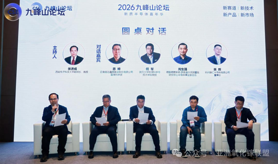
Zhang Jincheng — Vice President and Professor, Xidian University
Hui Feng— Chief Scientist, Yunnan Lincang Xinyuan Germanium Industry Co., Ltd.
He Jun— Professor, School of Physics and Technology, Wuhan University
Zhou Shengqiang— Director, Semiconductor Division, Helmholtz-Zentrum Dresden-Rossendorf (HZDR), Germany
Zhang Hui — Chairman, Hangzhou Garen Semiconductor Co., Ltd.
What Are the Key Bottlenecks in Technological Breakthroughs and Commercialization of Critical Compound Semiconductor Materials such as Germanium and Gallium?
Hui Feng: Germanium is a first-generation semiconductor with a relatively high level of technological maturity. China has established a complete industrial chain covering substrates, epitaxy, solar cells, and packaging, and is in a relatively strong position globally. As satellite demand continues to grow, a key priority is to further reduce costs while maintaining the radiation resistance and high- and low-temperature tolerance of multijunction solar cells. Gallium arsenide and indium phosphide are second-generation semiconductors. As early as 1962, the Institute of Semiconductors of the Chinese Academy of Sciences produced China’s first GaAs single crystal. The domestic industry has since largely overcome key technological barriers to commercialization, with device applications also representing a major strength of China’s semiconductor industry.
He Jun: You mentioned germanium as a substrate material for tandem solar cells. I remember that when I was at UCLA, Intel had a project on III–V tandem solar cells, and the efficiency was extremely high—reportedly reaching above 90%.
Hui Feng: In a typical triple-junction solar cell, germanium serves as the substrate, with the first subcell grown on the germanium substrate, followed by a GaAs subcell and then a GaInP subcell. The key challenge remains lattice matching.
Zhang Hui: There is no fundamental shortage of raw materials for the Ga₂O₃ industry. China accounts for more than 90% of global gallium raw material production, and most downstream application scenarios are also located in China. The current bottleneck is concentrated on the materials side. Ga₂O₃ substrates can already be produced, but epitaxial wafers remain a key hurdle. Once epitaxy is overcome, the entire industrial chain will be able to operate more smoothly. Over the next one or two years, the priority is to establish the overall industrial framework; once that foundation is in place, subsequent development should proceed more efficiently.
Zhou Shengqiang: My personal impression is that China is clearly ahead in Ga₂O₃. I attended the German Physical Society (DPG) annual conference, where there may have been fewer than 10 presentations on Ga₂O₃. Yet during these two days alone, the number of invited presentations on Ga₂O₃ has already exceeded 10. In China, research spanning materials through device design is already at the global forefront. I also conduct some fundamental research related to germanium. For n-type doping of germanium, we use ion implantation followed by a specialized short-duration annealing process.
How Can We Better Bridge Fundamental Research, Device Development, and Market Applications?
Hui Feng: I previously worked at the Institute of Semiconductors of the Chinese Academy of Sciences, where I spent more than 20 years conducting research and development on gallium arsenide and gallium phosphide. Commercialization must be built on a solid foundation of fundamental research. Without that foundation, it is difficult to resolve the technical challenges that arise during the commercialization process. Yunnan Lincang Xinyuan Germanium Industry has established strategic collaborations with the Institute of Semiconductors of the Chinese Academy of Sciences, Huawei, Jiufengshan Laboratory, and several universities, leveraging expert teams to address key challenges in industrialization.
He Jun: Not all technological research needs to be directly translated into market applications. Some research can instead accumulate as knowledge and contribute to talent development, providing a foundation for future technological breakthroughs.
Zhou Shengqiang: Germany also places great importance on industry–academia–research collaboration. A few years ago, we established a dedicated technology incubation office to encourage researchers to engage with companies and promote the transition of research achievements into market applications.
Zhang Hui: Much of the research on semiconductor single crystals will eventually become the responsibility of companies. As government funding gradually declines, universities increasingly need to rely on spin-off companies focused on commercialization to reinvest in and sustain research in established fields. The core of industry–academia–research collaboration is having a shared objective.
Zhang Jincheng: Fundamental research achievements ultimately have two destinations: they either “go onto the bookshelf” or “go onto the shelf.” Knowledge that goes onto the bookshelf can be preserved and developed within academia, while research achievements that are meant to go onto the shelf need to be advanced through technology transfer and commercialization. Today, the industrial ecosystem around Jiufengshan Laboratory and the East Lake High-tech Development Zone is showing increasingly strong momentum.
What Directions Should Compound Semiconductor Materials Focus on During the 15th Five-Year Plan Period?
Hui Feng: Under the 15th Five-Year Plan, semiconductors and information optoelectronics are among the key areas for development. Semiconductor single crystals are the foundation, and the development of large-diameter single-crystal materials remains a long-term priority. As crystal sizes increase, ensuring and maintaining material performance becomes critical. In addition, stronger industry–academia–research collaboration is needed to avoid repeating the lessons of the past, when the LED and photovoltaic industries experienced excessive investment and destructive competition. Coordinated efforts across academia and industry are essential to overcoming key technological challenges.
He Jun: In the RF sector, development will increasingly target 6G, interstellar communications, and defense applications. The optoelectronics sector encompasses various sensing technologies as well as automotive-grade applications for new energy vehicles. Leading domestic universities, including Northwestern Polytechnical University and Xidian University, have already established international influence in device and system applications, addressing markets potentially worth hundreds of billions or even trillions of yuan.
Zhang Hui: Ga₂O₃ needs to leverage its own strengths and target ultra-high-voltage and ultra-high-power applications. Epitaxy is the critical bridge connecting materials with devices. As substrates become increasingly affordable and their quality continues to improve, epitaxy will remain the key link connecting substrates to functional devices.
Zhang Jincheng: Looking toward the 15th Five-Year Plan, we need to continuously improve material and device performance, reduce costs, and accelerate the translation of academic achievements into industrial applications. The combined growth of artificial intelligence and new energy vehicles, together with the broader post-Moore era, is creating substantial opportunities for compound semiconductors. With enormous market demand ahead and growing international competition, we must strengthen independent technological development. Through collective efforts, China’s compound semiconductor materials industry is well positioned to achieve further progress during the 15th Five-Year Plan period.
Instruction
Official Account

Cooperation
Top
