


Major Breakthrough
Fujian-based Sunwise Semiconductor has achieved a major breakthrough in silicon-based heteroepitaxial gallium oxide piezoelectric thin-film materials, with its products now entering the customer validation stage. The material has demonstrated performance superior to that of conventional piezoelectric materials used for bulk acoustic wave (BAW) devices.
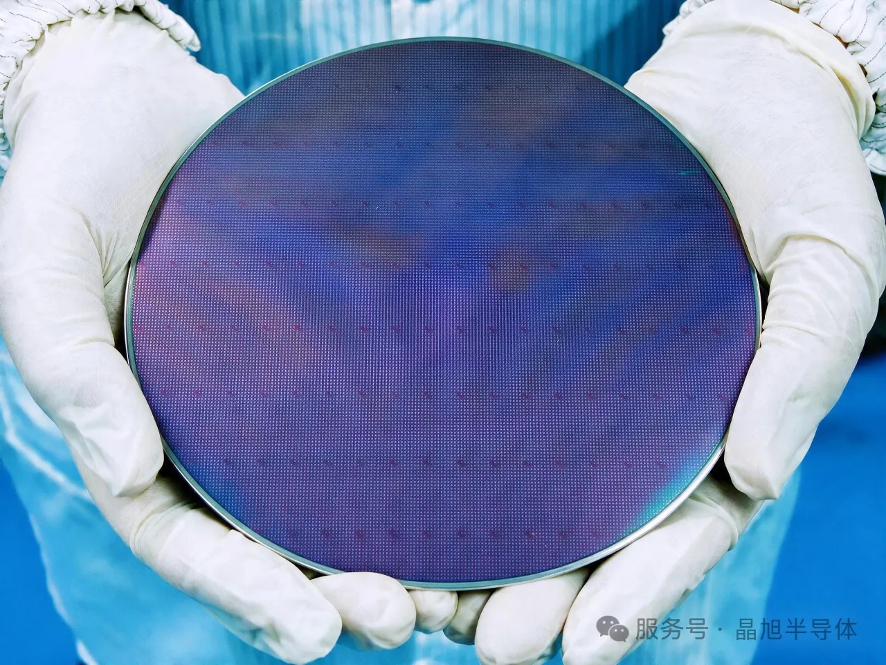
Bulk acoustic wave (BAW) filters are key components in RF front ends and are widely regarded as a representative technology for high-frequency, low-loss, and high-power acoustic filtering. With the continued expansion of 5G applications, high-frequency, wide-bandwidth BAW filters have evolved from an “optional component” into an essential core device, serving as a critical foundation for advances in next-generation wireless communications, radar sensing, satellite Internet, and other applications.
Unlike conventional AlN-based technology routes used in China and abroad, Sunwise Semiconductor has achieved a number of proprietary breakthroughs spanning gallium oxide materials, device design, manufacturing, and equipment. The company holds more than 100 granted invention patents in China and overseas, with key performance metrics reportedly exceeding those of comparable overseas products by more than 20%.
The company focuses on applications including 5G/6G communications, intelligent IoT, and high-precision positioning, and has developed globally competitive products such as epitaxial gallium oxide piezoelectric materials and POI wafers based on gallium oxide piezoelectric thin films. According to the company, Sunwise Semiconductor is currently the only company worldwide with in-house mass-production and delivery capabilities for gallium-oxide-based piezoelectric materials used in BAW filters.
Industry Challenges
Currently, AlN is the dominant piezoelectric material used in high-performance bulk acoustic wave (BAW) filters. The filter-device architectures built around AlN-based piezoelectric materials are subject to substantial intellectual property barriers, with key patents reportedly concentrated among companies in the United States, Japan, and other countries.
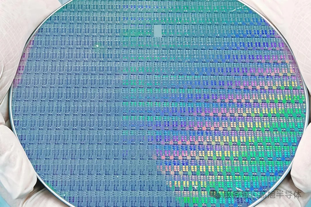
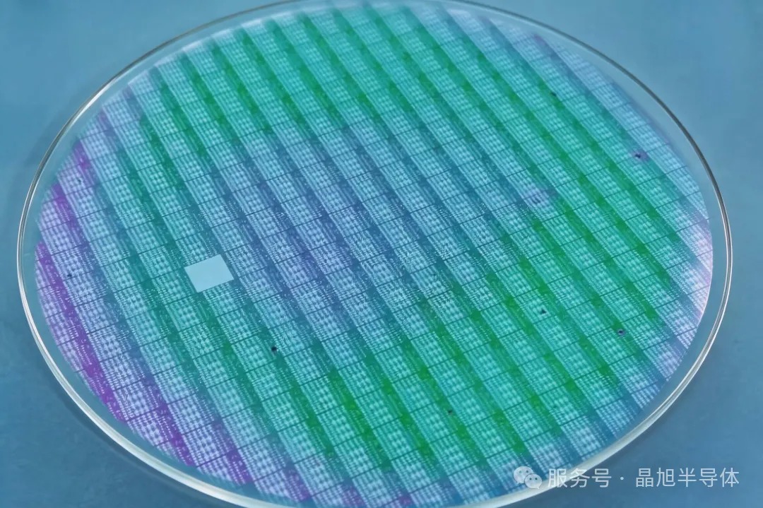
After more than 20 years of dedicated research, Sunwise Semiconductor overcame key commercialization barriers for silicon-based heteroepitaxial ε-Ga₂O₃ piezoelectric thin films in 2023. The company has developed a series of innovations spanning hardware, process technologies, software, and theoretical approaches, providing an alternative to the conventional AlN technology route and seeking to address overseas technology and IP barriers at the underlying material level.
Technological Breakthrough
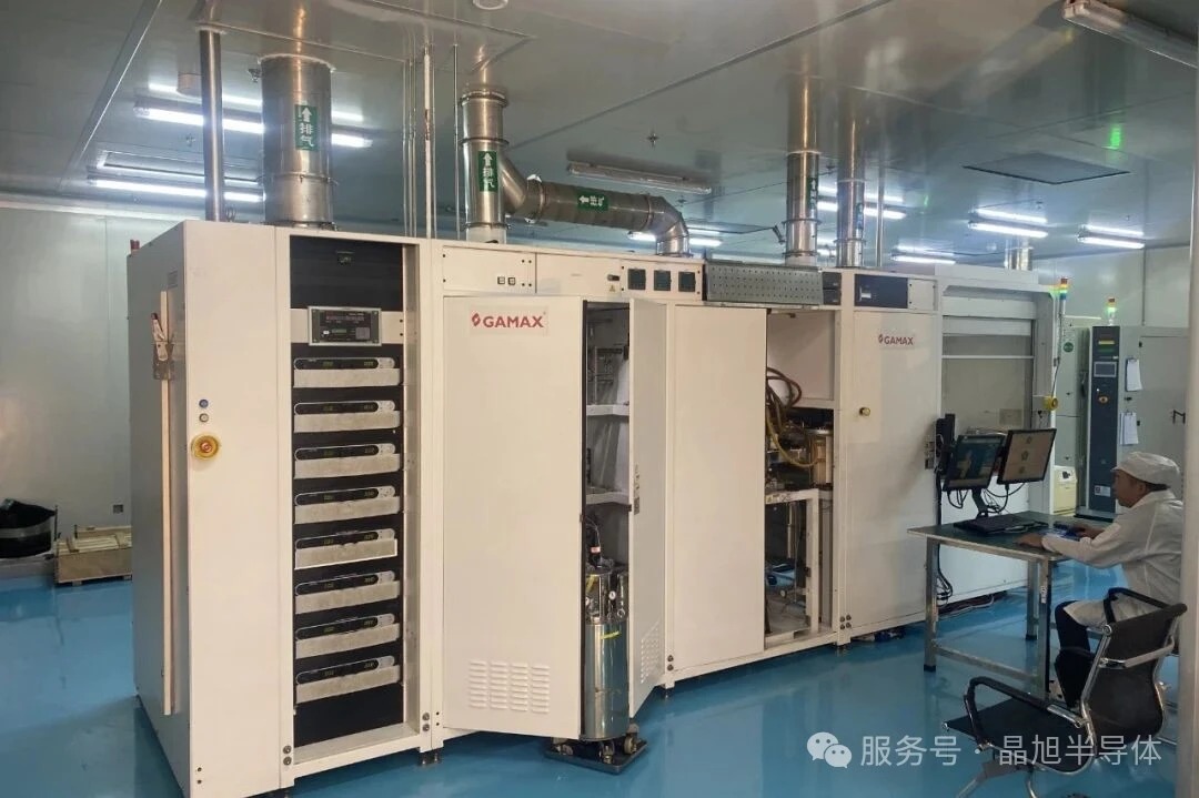
Development of the World’s First MOCVD System for Epitaxial ε-Ga₂O₃ Piezoelectric Thin Films
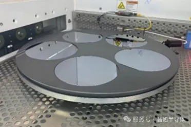
Through independent R&D and substantial investment in personnel and resources, Sunwise Semiconductor has successfully developed what it describes as the world’s first MOCVD system specifically designed for the growth of epitaxial ε-Ga₂O₃ piezoelectric thin films.
The company has overcome several key technical challenges, including computational-fluid-dynamics-assisted reactor flow-field and thermal-field design, as well as high-temperature oxidation-resistant heating technology. These developments have been incorporated into a proprietary MOCVD platform supported by a number of core patents, enabling the growth of high-quality ε-Ga₂O₃ piezoelectric thin films.
The resulting films reportedly achieve a rocking-curve FWHM below 0.6°, thickness uniformity better than 2%, and stress below 500 MPa. In terms of material quality, the films exhibit a c-axis orientation above 98%, porosity below 0.1%, and a dislocation density below 10⁶ cm⁻², with fewer internal defects than comparable piezoelectric materials. According to the company, these performance metrics meet the requirements for potential mass-production applications.
POI Wafers Based on ε-Ga₂O₃ Piezoelectric Materials
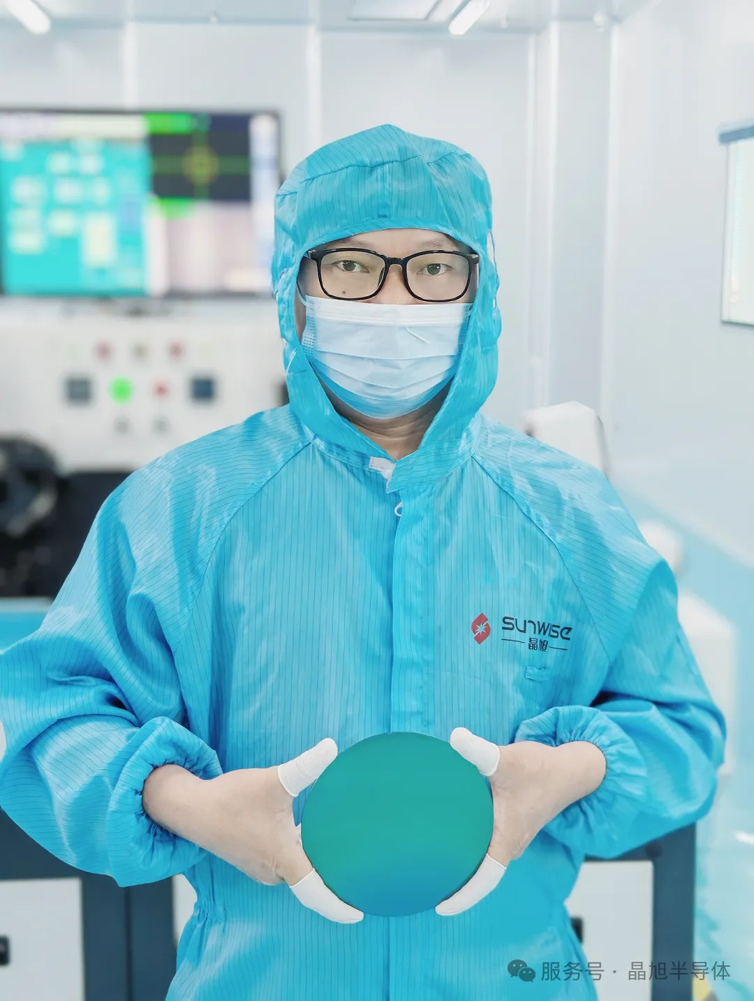
Building on high-quality ε-Ga₂O₃ piezoelectric thin-film materials, Sunwise Semiconductor has developed key processing technologies for the transfer fabrication of ε-Ga₂O₃ piezoelectric thin films and the formation of the bottom electrode, a critical layer in BAW filter structures. These processes enable the fabrication of POI wafers based on ε-Ga₂O₃ piezoelectric materials, achieving an overall yield of more than 97%, meeting the requirements for mass production.
POI wafers based on ε-Ga₂O₃ piezoelectric materials can support the following filter design specifications:
High operating frequency:2–10 GHz
Wide bandwidth:100 MHz–1.5 GHz
Ultra-low in-band insertion loss (single-crystal material):<2 dB
Power handling capability: Up to 2× that of conventional BAW filters
Commercialization Breakthrough
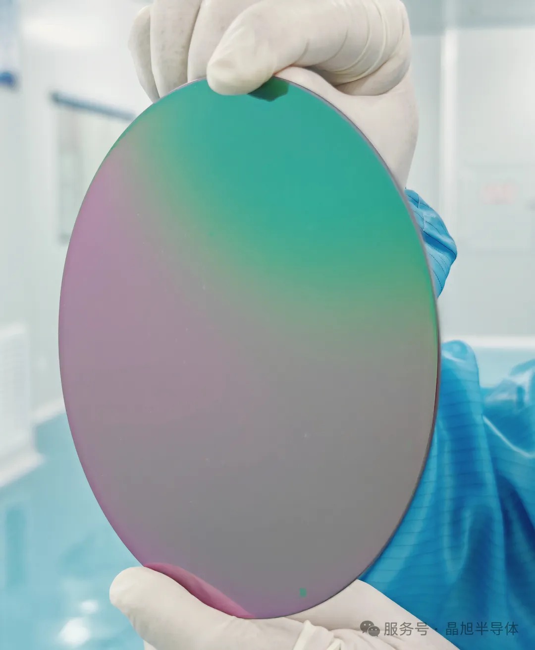
At present, Sunwise Semiconductor’s ε-Ga₂O₃ piezoelectric thin-film epitaxial wafers and POI wafers have received recognition from downstream Fabless companies, IDMs, and foundries in China and are gradually entering the customer validation stage. Mass delivery is expected to begin by the end of 2026. Recent customer validation results indicate that filters based on ε-Ga₂O₃ piezoelectric materials demonstrate notable advantages in low loss and wide-bandwidth applications.
The company’s silicon-based heteroepitaxial growth approach also provides significant cost advantages. Compared with conventional wide-bandwidth piezoelectric materials produced through doping-based approaches, the cost of Sunwise Semiconductor’s ε-Ga₂O₃ piezoelectric material is reportedly around 50% lower. In addition, the epitaxial approach enables the production of large-area ε-Ga₂O₃ piezoelectric thin films. Sunwise Semiconductor expects to achieve 8-inch ε-Ga₂O₃ piezoelectric material epitaxial growth by the end of 2026, which is expected to further reduce production costs.

About Sunwise Semiconductor
Sunwise Semiconductor focuses on ultra-wide-bandgap semiconductor and optoelectronic integration technologies based on third-generation gallium nitride (GaN) and fourth-generation gallium oxide (Ga₂O₃) materials. The company is a high-tech enterprise with rare wafer-level heterogeneous and heterostructure integration capabilities in China.
Led by an academician-backed R&D team, Sunwise has developed proprietary technologies for single-crystal Ga₂O₃ thin-film epitaxy and wafer-level heterogeneous integration, with more than 100 core patents and a comprehensive portfolio of independently owned intellectual property.
Leveraging its advanced heterogeneous integration platform, Sunwise has established an end-to-end process chain covering epitaxial growth, damage-free thin-film release, wafer-level transfer and bonding, and optoelectronic integration and packaging. Its 8-inch-class wafer-level heterogeneous integration platform is aligned with the process requirements of optical communication modulator chips. The company has achieved volume production and delivery of GaN optoelectronic integration packaging, while its 6- and 8-inch Ga₂O₃ epitaxy and substrate-transfer product lines, including Ga₂O₃ POI wafers, are entering pilot production and ramp-up stages.
Looking ahead, Sunwise plans to extend its heterogeneous integration technologies to thin-film lithium niobate on insulator (LNOI) and silicon-on-insulator (SOI) platforms for AI computing optical modules. The company is committed to working with industry partners to address key bottlenecks in advanced semiconductor materials and devices, helping overcome international technology barriers and supporting the development of high-end chip materials and optical communication products. Its goal is to become a world-leading company in compound semiconductor materials R&D, manufacturing, and services.
Instruction
Official Account

Cooperation
Top
