


Recently, a team from the University of Hong Kong and Nanjing University published a review paper titled "Research Progress on Gallium Nitride and Gallium Oxide Semiconductor Avalanche Power Devices" in the journal "Acta Electronica Sinica". The research focuses on wide bandgap (GaN) and ultra-wide bandgap (Ga₂O₃) semiconductor power devices, systematically sorting out and exploring issues such as the avalanche breakdown physical mechanism, terminal electric field regulation, dynamic UIS avalanche tolerance, and repeatable avalanche capability of the devices under transient operating conditions such as sudden changes in inductive load and short-circuit faults.
Background
Wide Bandgap (WBG) and Ultra-wide Bandgap (UWBG) semiconductors have attracted significant attention for next-generation power electronics due to their higher critical electric fields, wider bandgaps, and superior high-temperature stability. These properties enable power devices to operate efficiently and reliably under high-voltage, high-frequency, and high-power-density conditions. Among them, gallium oxide (Ga₂O₃) features an extremely high theoretical critical electric field of approximately 8 MV/cm and offers the potential for large-size, low-cost single-crystal substrates through melt-based growth, making it a promising candidate for next-generation high-voltage power devices. However, Ga₂O₃ still faces challenges such as the difficulty of achieving p-type doping and the resulting inability to readily form homojunction avalanche p–n junctions, while heterojunctions suffer from issues including interface defects and electric-field crowding, which limit device performance and reliability.
Meanwhile, under transient conditions such as inductive load switching, short-circuit faults, electromagnetic interference pulses, and high dv/dt and di/dt stresses, power devices may need to withstand avalanche breakdown and absorb and dissipate transient energy. As a result, avalanche capability has become a key indicator of the safe operating area and system robustness of high-voltage power devices. Focusing on the goal of achieving repeatable and robust avalanche operation, this article systematically reviews the physical mechanisms underlying avalanche breakdown in WBG and UWBG power devices, as well as quantitative characterization and evaluation methods. Particular attention is given to static breakdown, dynamic unclamped inductive switching (UIS) avalanche testing, and avalanche energy evaluation. The article further examines the synergistic roles of electric-field uniformization and avalanche ionization from the perspective of termination and edge-structure design.
At the device level, the review summarizes recent progress in the avalanche endurance and repeatable avalanche performance of GaN vertical diodes, Fin-JFET transistors, and Ga₂O₃ heterojunction power devices, with particular emphasis on key technologies including heterojunction termination electric-field control, minority-carrier transport at interfaces, and highly reliable overvoltage surge protection. Finally, based on recent research advances, the article discusses future directions including material–device–circuit co-design and modeling of avalanche behavior, highly robust termination and composite structural design, system-level avalanche reliability under complex operating conditions, and the coupled evolution of avalanche failure and thermal effects. These insights provide guidance and reference for the design, evaluation, and engineering application of next-generation high-voltage, highly reliable power devices.
Abstract
This paper systematically reviews the research progress of avalanche power devices based on wide-bandgap gallium nitride (GaN) and ultra-wide-bandgap gallium oxide (Ga₂O₃) semiconductors, with the core objective of achieving "repeatable and robust avalanche" operation in power devices. The paper first elucidates the physical mechanism of carrier multiplication in avalanche breakdown and multidimensional characterization methods including static I–V and dynamic unclamped inductive switching (UIS) tests, emphasizing the critical role of termination structures in electric-field homogenization. Subsequently, it focuses on the technical pathways by which GaN vertical diodes and Fin-JFET transistors achieve high avalanche ruggedness through termination optimizations such as ion-implanted guard rings, gradient junction termination extension (JTE), beveled mesa, and ultra-small-angle bevel JTE (USAB-JTE), covering the evolution from native GaN substrates to low-cost patterned sapphire substrates (PSS). To address the bottleneck of difficult p-type doping in Ga₂O₃, it summarizes the breakthrough progress in realizing "high-voltage, high-current, high-robustness" avalanche operation through p-NiO/n-Ga₂O₃ heterojunctions combined with beveled JTE and high-permittivity field plates. Finally, it outlines future directions including material–device–circuit co-design modeling, composite termination design, system-level reliability evaluation, and failure-mechanism research, providing guidance for the design of next-generation high-voltage, high-reliability power devices.
Conclusion
The core conclusion of this review is that wide-bandgap and ultra-wide-bandgap avalanche power devices have advanced from merely demonstrating "avalanche capability" to a new stage of "robust and repeatable avalanche" operation, marking a substantive breakthrough in their reliability and engineering practicality.
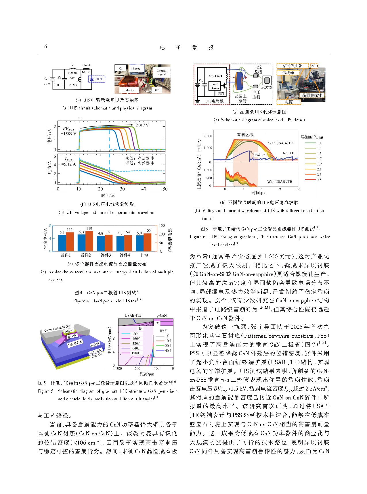
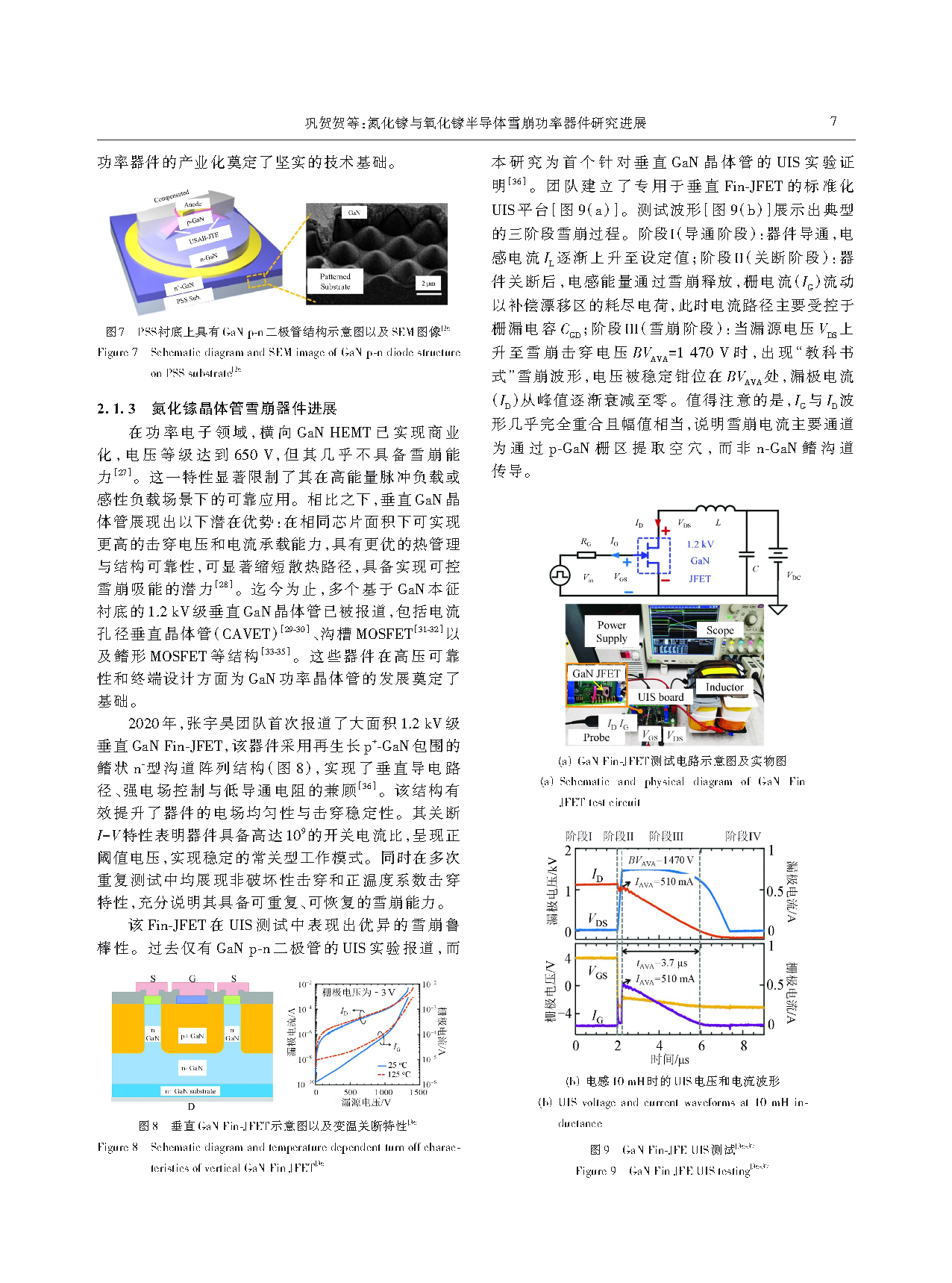
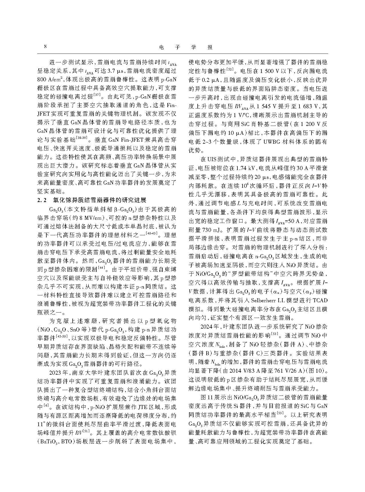
In the GaN system, device avalanche capability has achieved a leap from "feasible" to "designable." Through multidimensional termination optimizations including ion-implanted guard rings, gradient junction termination extension (JTE), beveled mesa, and ultra-small-angle bevel JTE (USAB-JTE), the avalanche energy density (EAVA) of 1–2 kV-class vertical GaN p-n diodes has surpassed the J/cm² level, reaching as high as 7.56 J/cm². Among these, gradient JTE devices achieved an avalanche breakdown voltage of 1.7 kV and an avalanche current density exceeding 1100 A/cm² without thermal failure, while the low-cost patterned sapphire substrate (PSS) route realized a BVAVA greater than 1.5 kV and an IAVA exceeding 2 kA/cm², with avalanche ruggedness approaching that of native GaN substrates. Vertical GaN Fin-JFETs also demonstrated transistor-level avalanche capability for the first time through UIS experiments, with a breakdown voltage of 1470 V and an avalanche current density exceeding 800 A/cm², revealing the key physical mechanism that the p-GaN gate region serves as the primary channel for hole extraction during avalanche.
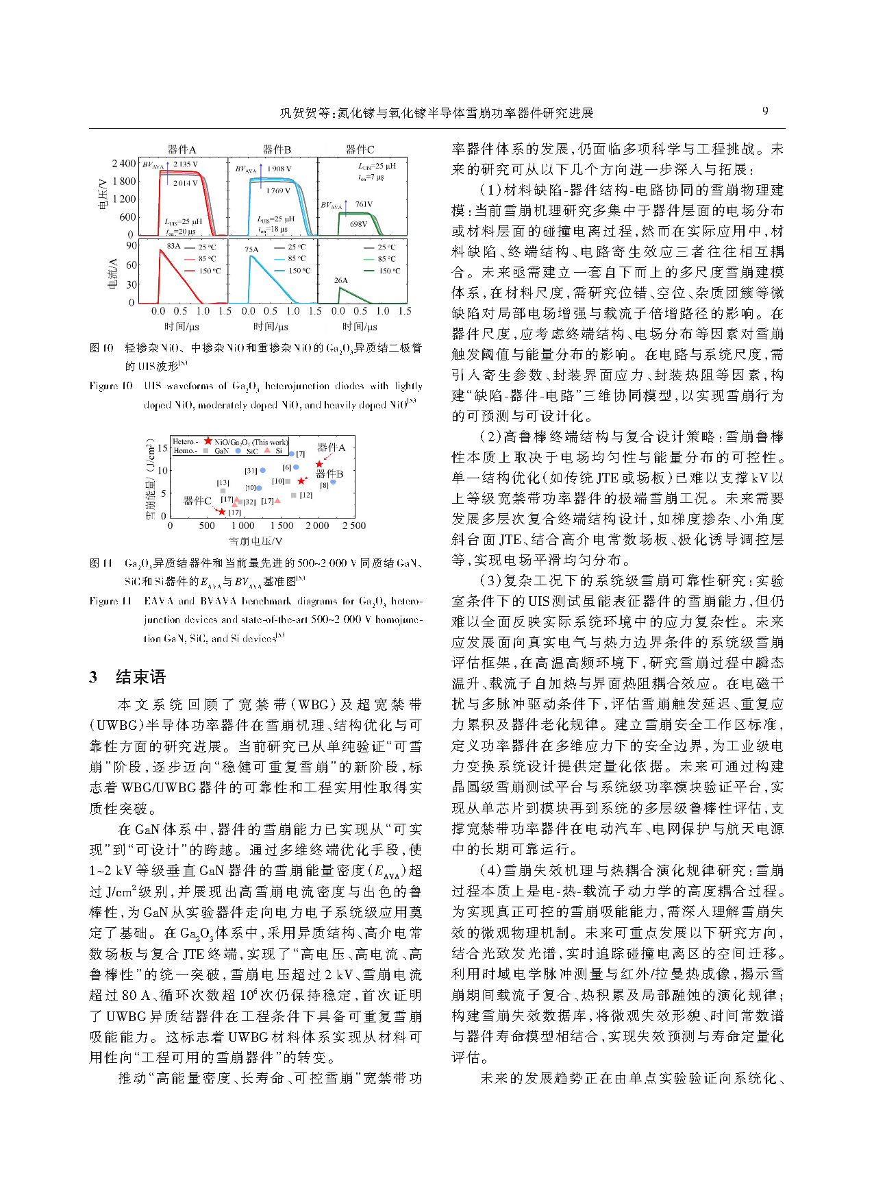
In the Ga₂O₃ system, researchers adopted a p-NiO/n-Ga₂O₃ heterojunction combined with a composite terminal scheme of beveled JTE and a high-permittivity BaTiO₃ field plate, achieving a unified breakthrough of "high voltage, high current, and high robustness." The devices exhibited an avalanche voltage exceeding 2 kV (up to 2.1 kV), an avalanche current exceeding 80 A (up to 83 A), and a single-pulse avalanche energy of 730 mJ, with virtually no drift in forward and reverse I–V characteristics after 10⁶ consecutive cycles—demonstrating for the first time that ultra-wide-bandgap heterojunction devices possess repeatable avalanche energy absorption capability under engineering conditions. Their avalanche energy density is comparable to the highest levels reported for state-of-the-art SiC and GaN homojunction devices, far exceeding that of conventional Si devices. Physically, impact ionization was confirmed to occur in the n-Ga₂O₃ main junction region, while the "Rhombohedral-type band alignment" of the NiO/Ga₂O₃ interface enables barrier-free hole transport across the heterojunction, which is the key to sustaining high avalanche current.
Finally, the review points out that the field is evolving from single-point experimental verification toward systematic, multidimensional modeling and standardized testing. Future breakthroughs are needed in four directions: material-defect–device-structure–circuit co-design modeling, high-robustness composite terminal design, system-level reliability evaluation under complex operating conditions, and the electro-thermal coupling mechanism of avalanche failure.
Significance
For the first time, the review takes “repeatable and robust avalanche operation” as its central theme, systematically connecting the physical mechanisms of avalanche breakdown, including carrier multiplication, with multidimensional characterization methods and termination-structure design strategies. It also comparatively examines the distinct technological pathways adopted by GaN and Ga₂O₃ avalanche power devices, helping clarify the fundamental differences between the avalanche mechanisms of WBG/UWBG devices and those of conventional Si devices and establishing a unified framework for understanding avalanche behavior in this field.
The review further summarizes several key physical mechanisms that may offer valuable insights at the mechanistic level. For example, in vertical GaN Fin-JFETs, the p-GaN gate region serves as the primary pathway for avalanche-hole extraction, while the “Rhombohedral-type band alignment” of the NiO/Ga₂O₃ heterojunction supports high hole current transport. These mechanistic insights provide a theoretical basis for the more systematic and design-oriented development of future power-device structures.
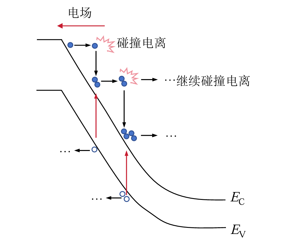
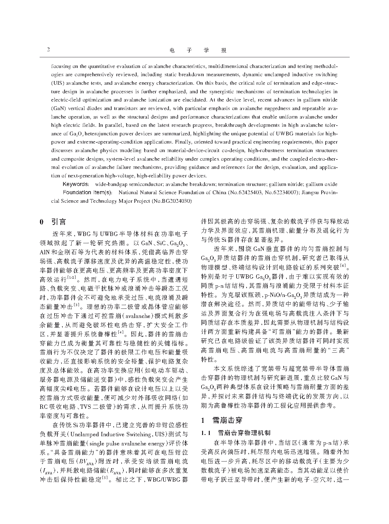
Figure 1 Schematic band diagram of avalanche multiplication in semi⁃ conductor p-n junction under reverse bias
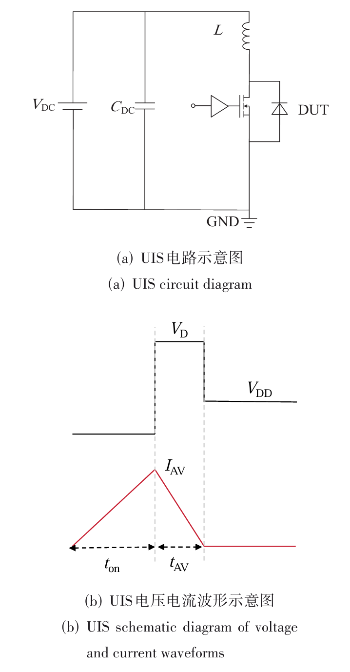
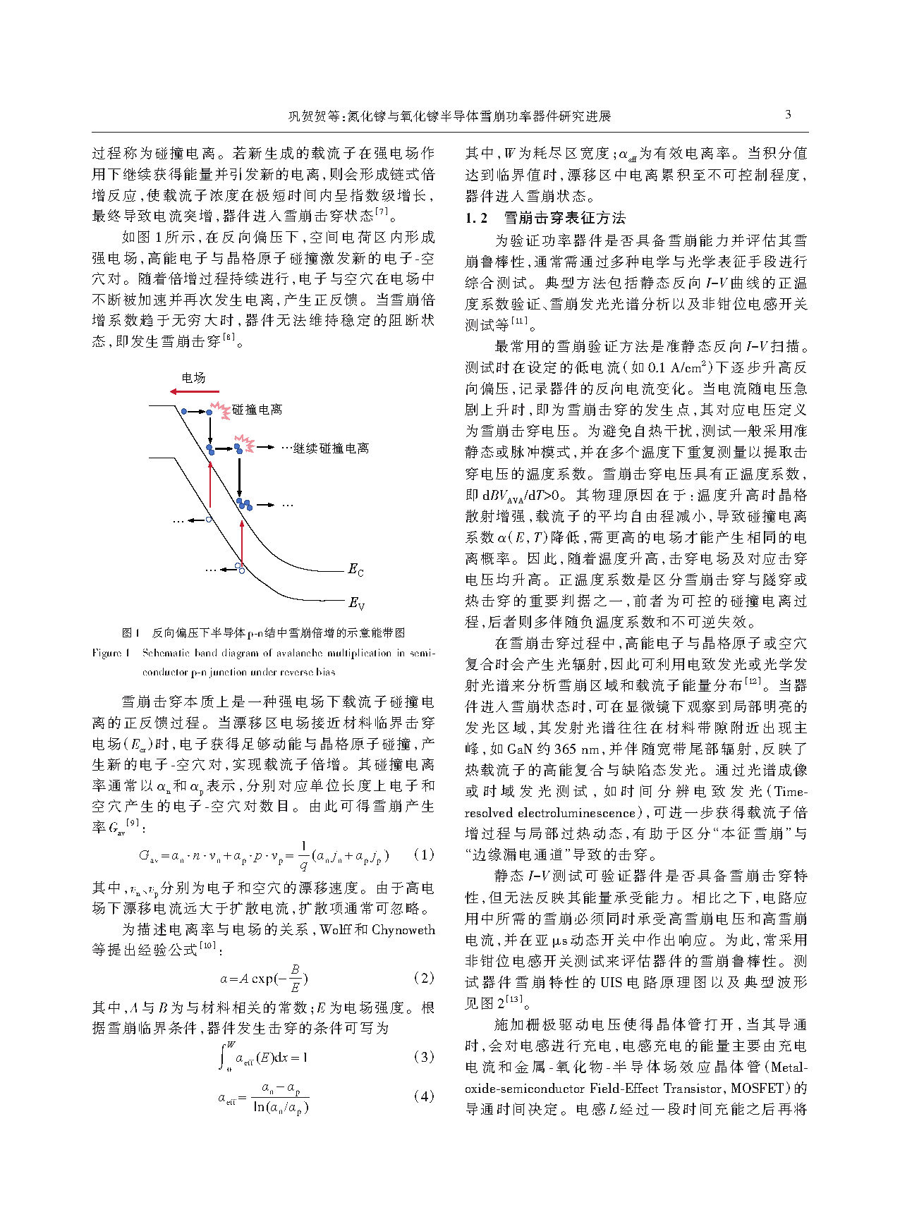
Figure 2 UIS circuit and waveform diagram
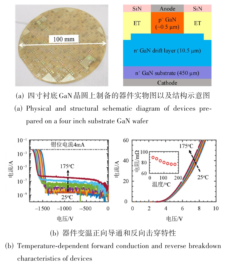
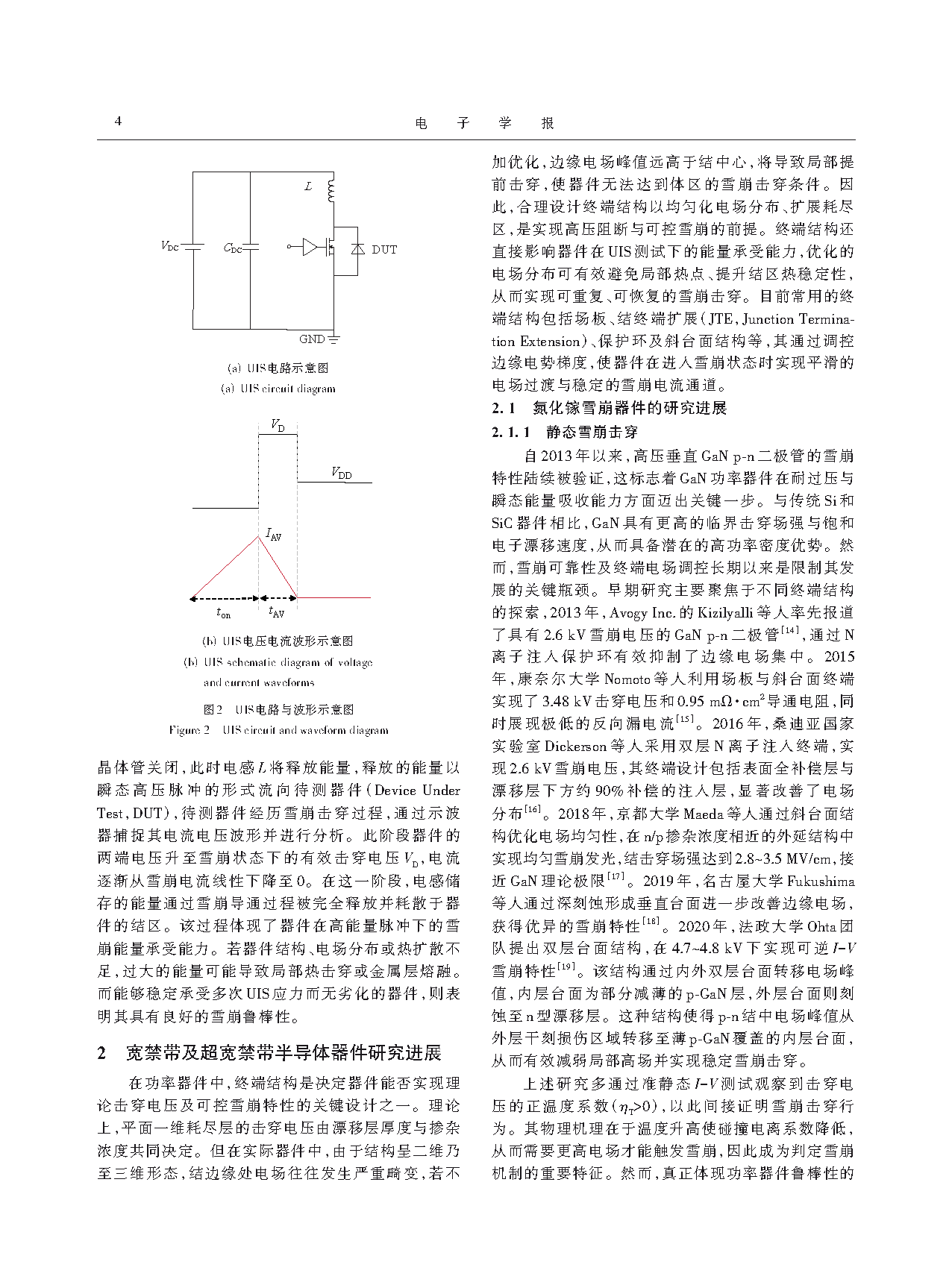
Figure 3 Structure and temperature-dependent characterization of vertical GaN diode devices
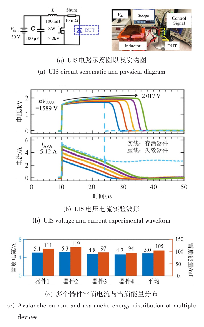
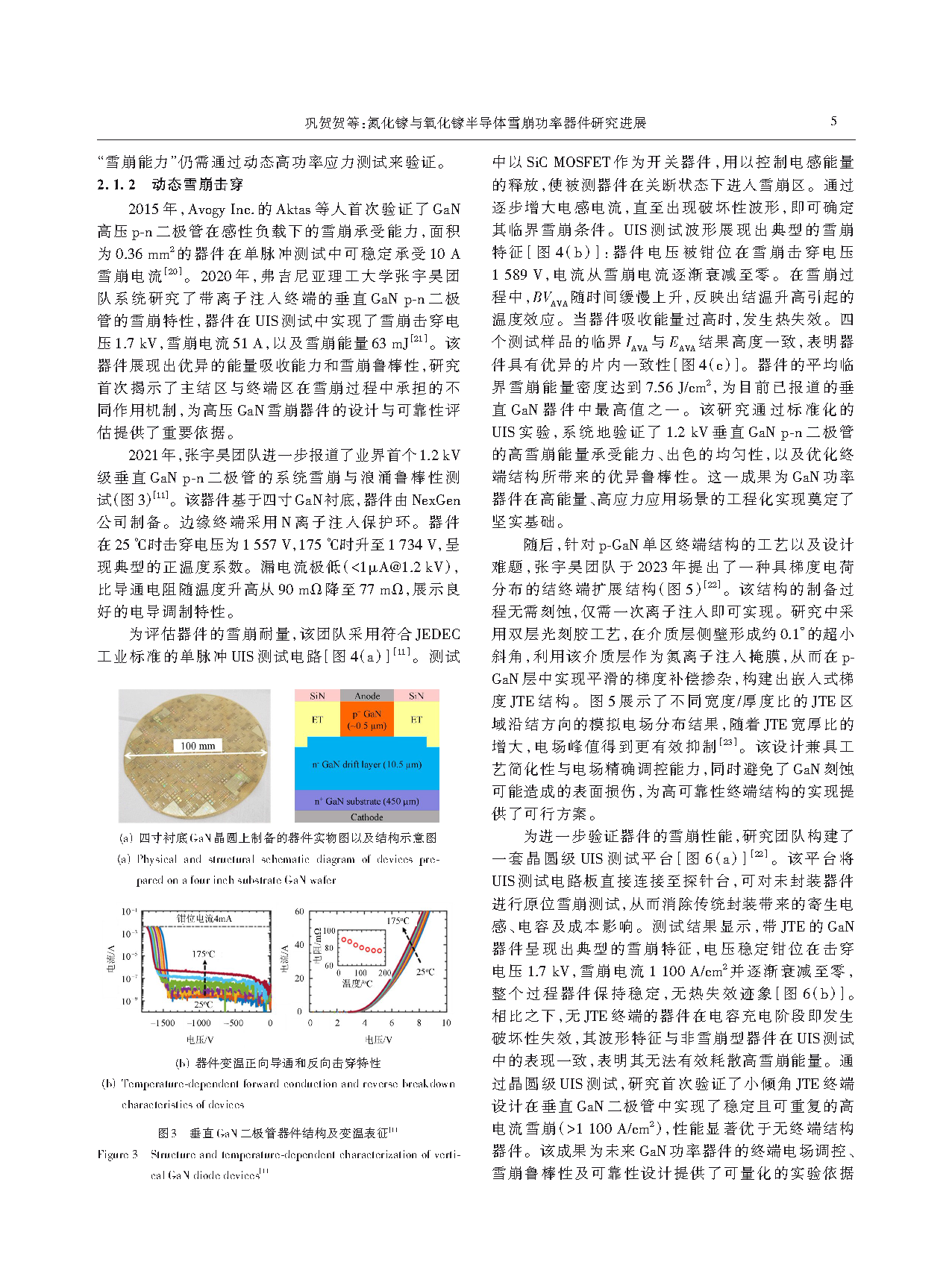
Figure 4 GaN p-n diode UIS test
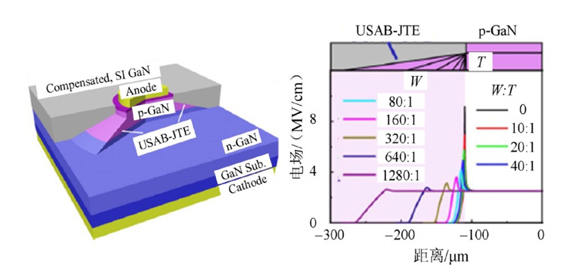
Figure 5 Schematic diagram of gradient JTE structure GaN p-n diode and electric field distribution at different tilt angles
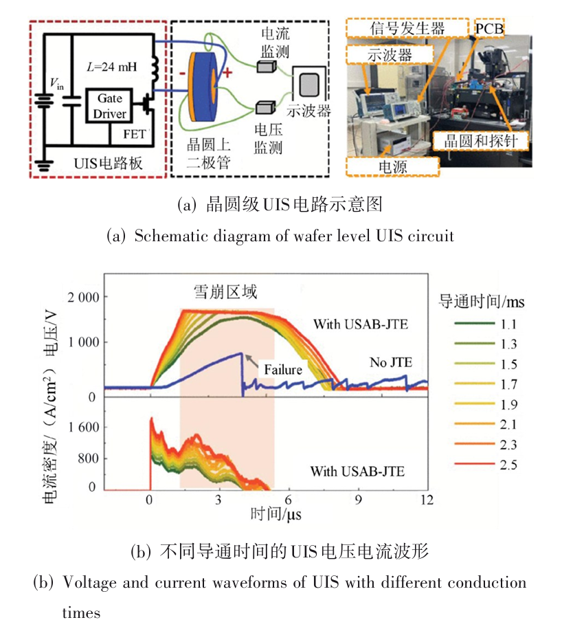
Figure 6 UIS testing of gradient JTE structured GaN p-n diode wafer level devices
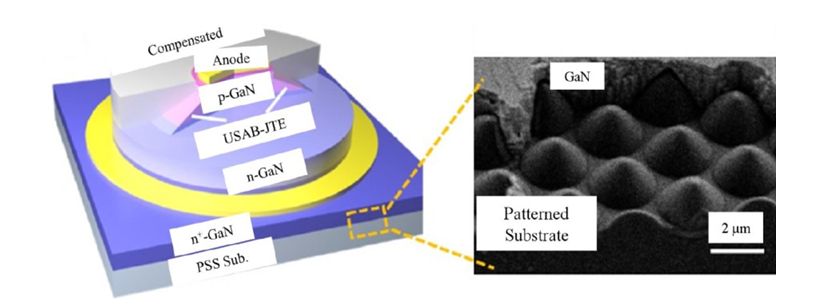
Figure 7 Schematic diagram and SEM image of GaN p-n diode structure on PSS substrate
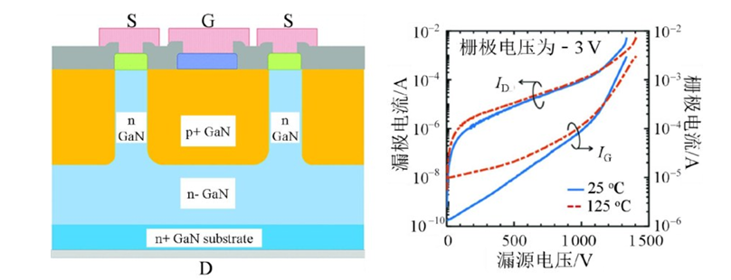
Figure 8 Schematic diagram and temperature dependent turn off charac⁃ teristics of vertical GaN Fin JFET
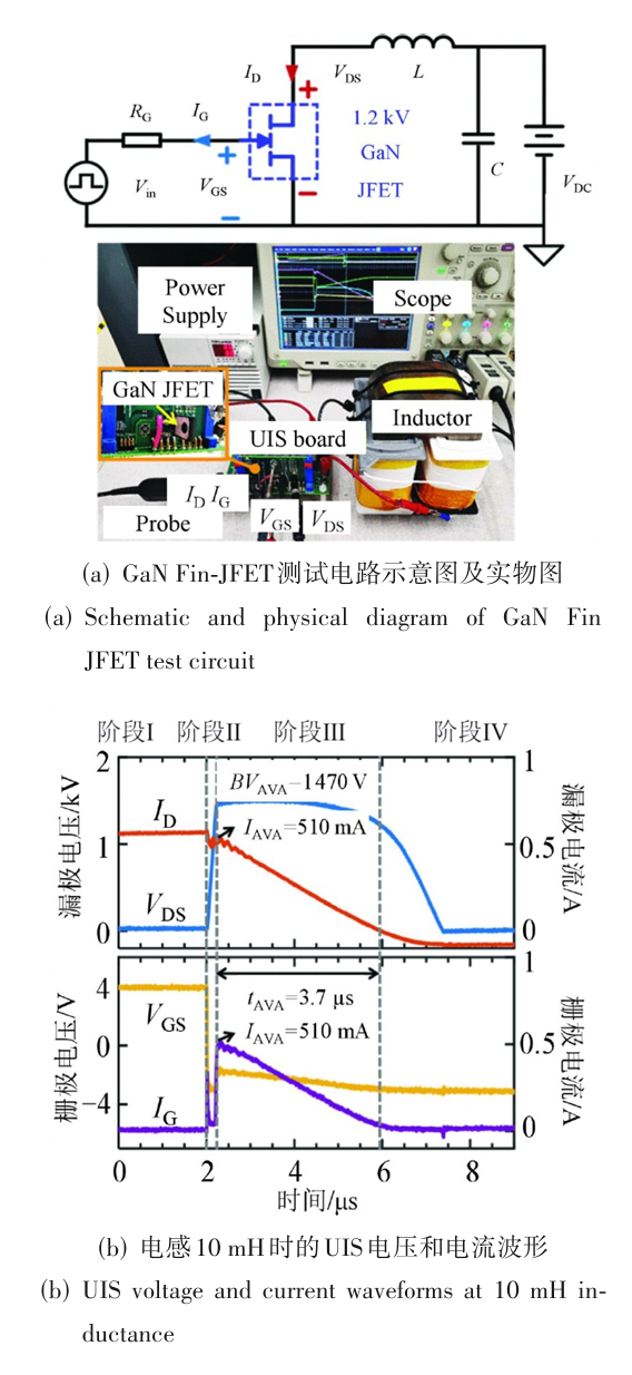
Figure 9 GaN Fin JFE UIS testing
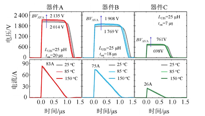
Figure 10 UIS waveforms of Ga₂O₃ heterojunction diodes with lightly doped NiO, moderately doped NiO, and heavily doped NiO
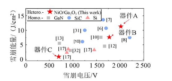
Figure 11 EAVA and BVAVA benchmark diagrams for Ga₂O₃ hetero⁃ junction devices and state-of-the-art 500~2 000 V homojunction GaN, SiC, and Si devices
DOI:
10.12263/DZXB.20251072

Instruction
Official Account

Cooperation
Top
