



Researchers from Shenzhen University, South China Normal University have published a dissertation titled "Ultrahigh-Performance Mix-Structure Ga₂O₃/ZnO Heterostructure Solar Blind UV Detector and Its Wide Applications in Multiples of Scenarios Under Different Conditions" in Small.
Background
Solar-blind ultraviolet (220–280 nm) photodetection technology plays an irreplaceable role in military secure UV communication, missile early warning, power grid fire monitoring, ozone detection and neuromorphic computing. As an ultra-wide bandgap semiconductor, β-Ga₂O₃ matches the solar-blind absorption band and can be fabricated into large-area films, making it ideal for UV detectors. Conventional single-phase Ga₂O₃ devices face a trade-off between high responsivity and fast response speed. High-gain devices suffer slow decay due to hole trapping, while fast devices lose sensitivity under weak UV light. Existing MSM and MOS-type Ga₂O₃ devices only adapt to single application scenarios. ZnO-based conductive layers can form heterojunctions with avalanche multiplication to boost device performance, but most studies focus on crystalline Ga₂O₃/ZnO systems. The multi-condition photoresponse mechanism of mix-structure Ga₂O₃/ZnO heterostructures remains unclear, and integrated detectors compatible with high-speed UV communication, weak-light alarm and artificial synapse simulation are rarely reported, forming an important research gap.
Abstract
Practical application of solar-blind UV (220–280 nm) detectors in multiples of fields is key problem in UV optoelectronic technology. Herein, the performance of mix-structure Ga₂O₃/ZnO Ga₂O₃/Ga doped ZnO hetero-structure detectors are firstly optimized, optimized mix-structure Ga₂O₃ detector possesses high response (3010.2 A/W@235 nm, 40 V), low Idark (6.97 ×10⁻¹¹ A @40 V), high IUV/Idark ratio (10⁵ at 4.8 μW/cm² 235 nm) simultaneously. The mechanisms of the device under different conditions are explored. Avalanche breakdown mechanism induced fast response and decay speeds (tr: 2.47 µs) at pulse UV laser in the device under high voltage, which favored its application in UV communications. Fast response and decay speeds of the device at faint 254 nm light (tr: 25.95 s: td1: 23.05 s), is beneficial for its application in missile alarm, electrical fire alarm, ozone alarm, and so on. Because of high density of Holes are trapped within the device under 1 V bias and faint deep UV condition, the mix-structure Ga₂O₃/ZnO heterostructure detector presented good performance in simulating complicated PPFLTP behavior of synapses in human brains and ANN. The difference response and recovery mechanism of the Ga₂O₃/ZnO hetero-structure detector under different conditions, is especially meaningful in actual applications of the device in various scenarios.
Highlights
A series of mix-structure Ga₂O₃/ZnO and Ga₂O₃/Ga-doped ZnO heterostructure solar-blind photodetectors are designed and fabricated for multi-scenario applications.
The optimized device achieves ultrahigh responsivity, ultra-low dark current and high photo-to-dark current ratio simultaneously under reverse bias.
Distinct avalanche breakdown and hole-trapping mechanisms are revealed under high voltage pulse UV and low-bias weak UV conditions respectively.
The single device realizes high-speed UV communication, weak-light early warning and artificial synaptic neuromorphic simulation three functions synchronously.
Conclusion
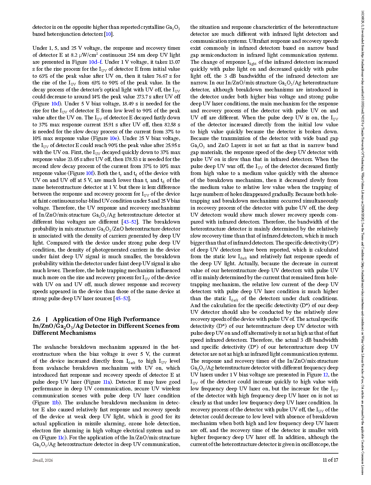
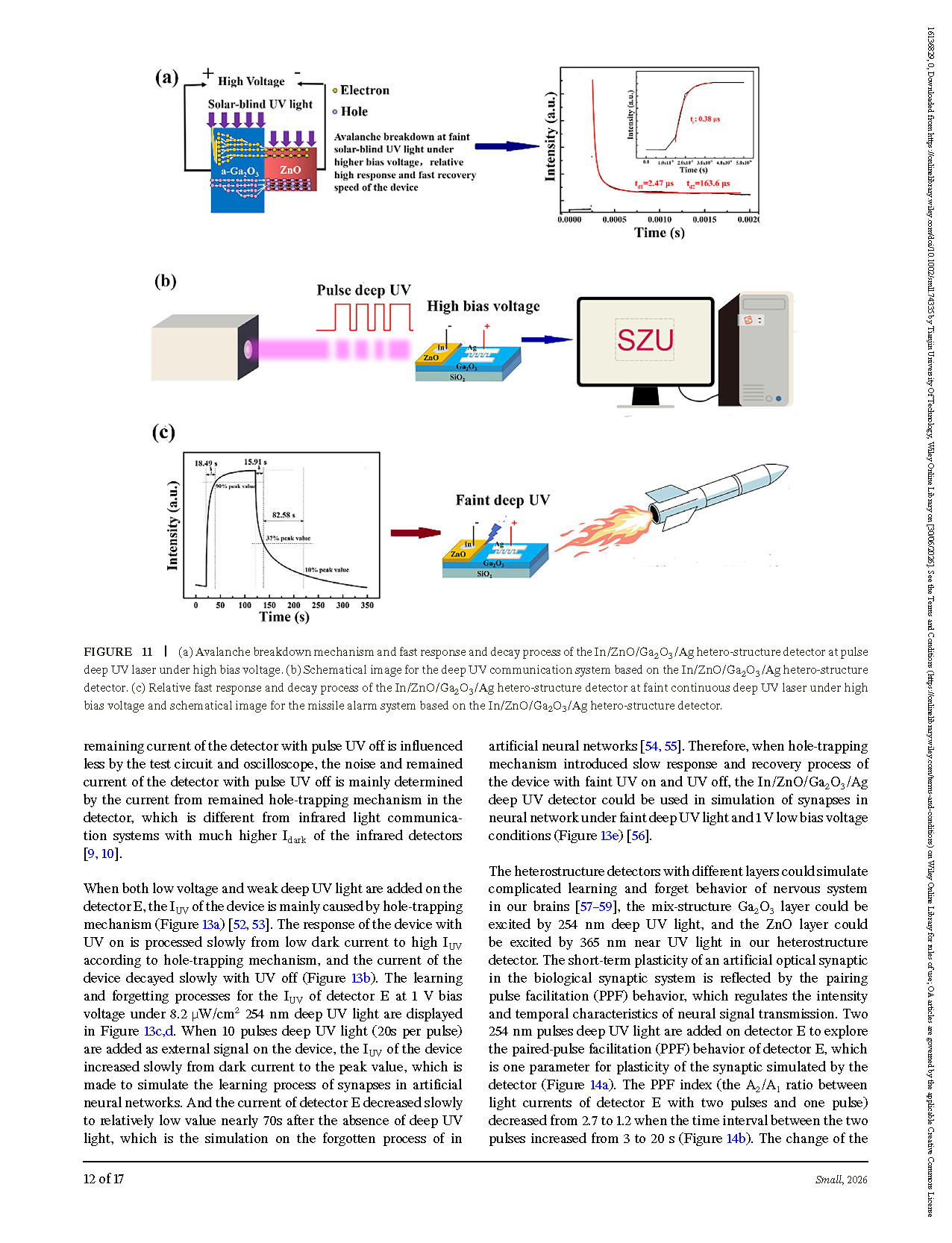
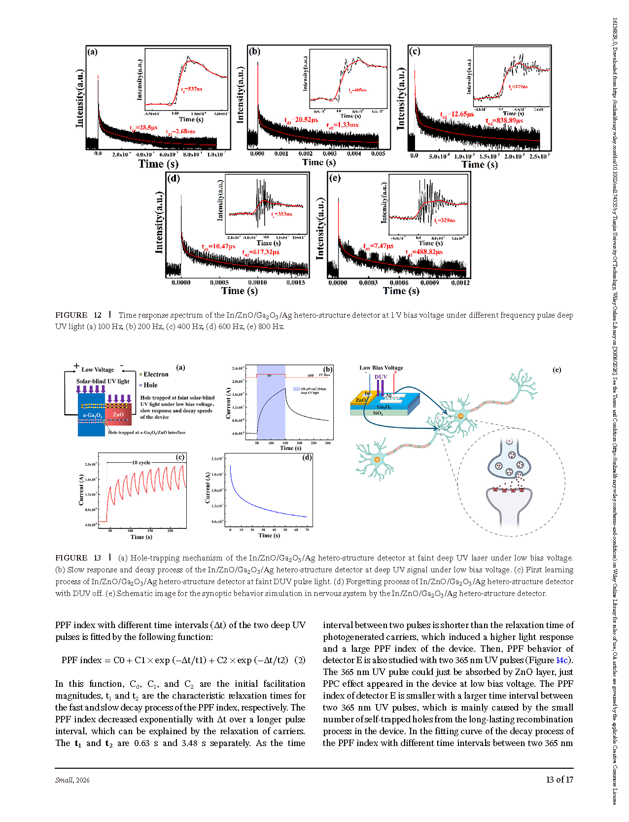
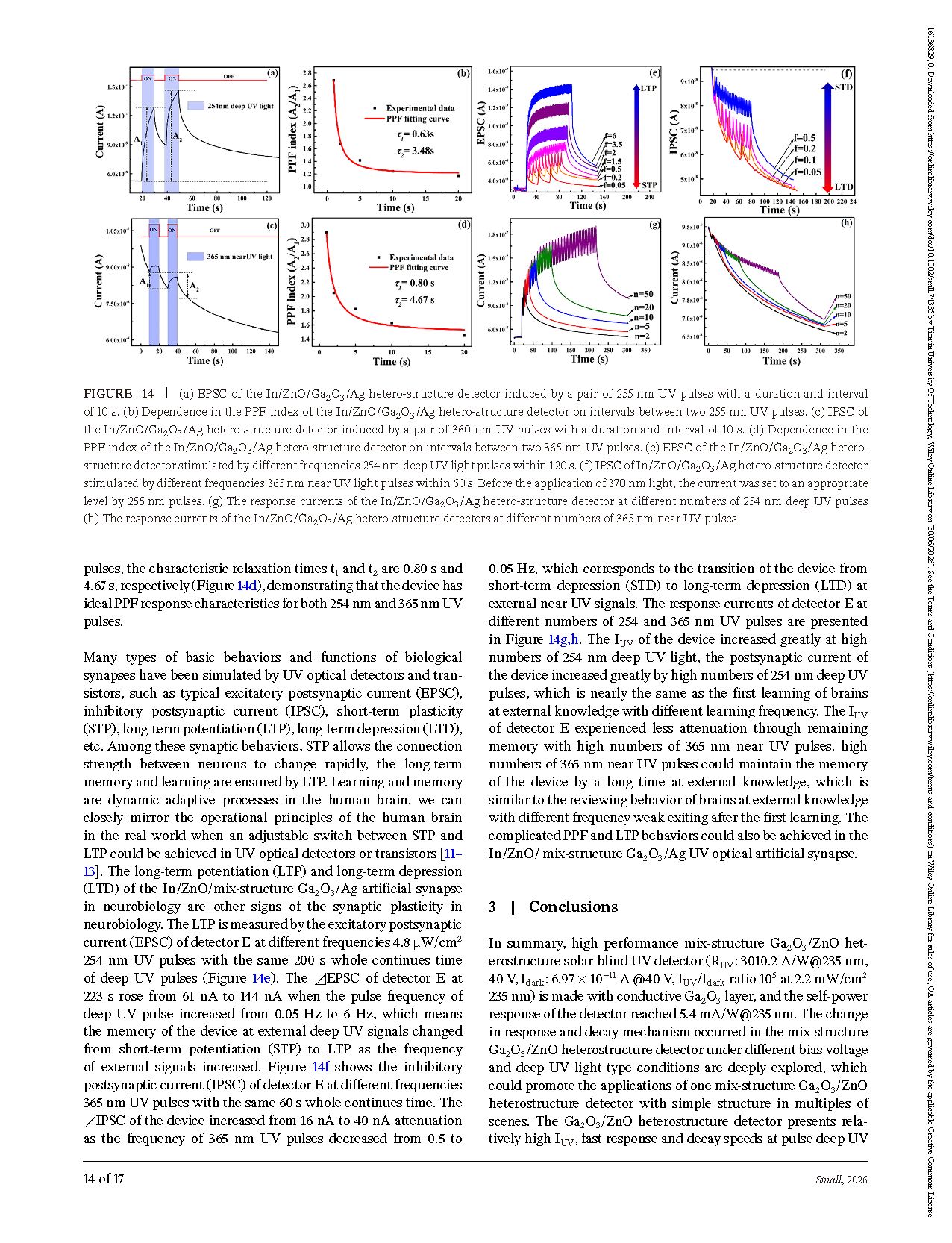
In summary, high performance mix-structure Ga₂O₃/ZnO heterostructure solar-blind UV detector (RUV: 3010.2 A/W@235 nm, 40 V, Idark: 6.97 ×10⁻¹¹ A @40 V, IUV/Idark ratio 10⁵ at 2.2 mW/cm² 235 nm) is made with conductive Ga₂O₃ layer, and the self-power response of the detector reached 5.4 mA/W@235 nm. The change in response and decay mechanism occurred in the mix-structure Ga₂O₃/ZnO heterostructure detector under different bias voltage and deep UV light type conditions are deeply explored, which could promote the applications of one mix-structure Ga₂O₃/ZnO heterostructure detector with simple structure in multiples of scenes. The Ga₂O₃/ZnO heterostructure detector presents relatively high IUV, fast response and decay speeds at pulse deep UV laser (tr: 0.38 ms: td1: 2.47 ms) at high bias voltage from avalanche breakdown mechanism, which is especially important in actual use in ultra-fast UV communication and secure wireless communication. The relatively high response, fast response and decay speeds (tr: 35.95 s: td1: 23.05 s) of the Ga₂O₃ detector at weak deep UV light, is beneficial for its application in missile alarming, ozone hole alarm, electrical fire alarm, and so on. Hole trapping mechanism introduced the slow response and decay process of the device under 1 V voltage at weak deep UV light, so the mix-structure Ga₂O₃/ZnO heterostructure detector could not only simulate learning and forgot process of synapse in artificial neural network, but also could be selected as key device to simulate the complicated behavior of human brains (PPF, LTP, LTD first learning, reviewing behavior). This is especially meaningful in establishment of new generation artificial neural network and neural network computation system based on deep UV optoelectronic devices.
Project Support
This work was supported by the National Natural Science Foundation of China under Grant No. (51872187, 12074263, 11774241, 51371120, 51302174, 61704111, 62571201), Guangdong Basic and Applied Basic Research Foundation (2021A1515012013), the Science and Technology Research Items of Shenzhen (JCYJ20170818144255777, JCYJ20170818144212483, JCYJ20180507182248925, JCYJ2016022619203302). This work received partial support from the National Natural Science Foundation of China (Nos. 62571201).
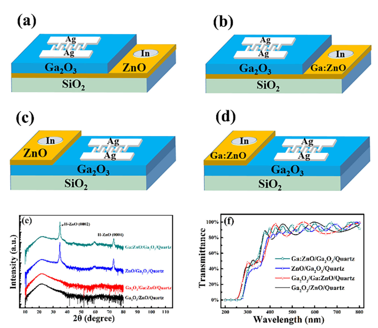
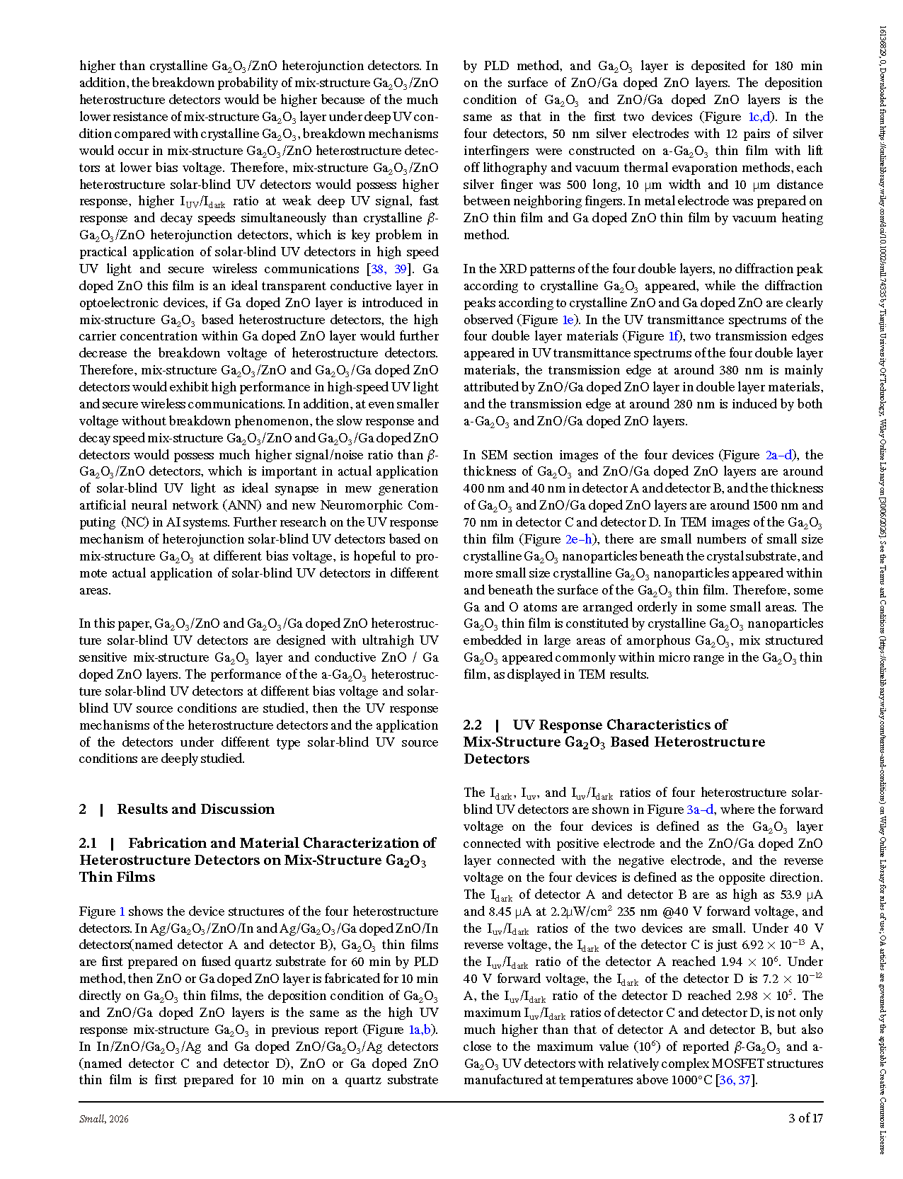
FIGURE 1 The structures of the four hetero-structure solar-blind UV detectors. (a) Ag/Ga₂O₃/ZnO/In hetero-structure solar-blind UV Photodetector. (b) Ag/Ga₂O₃/Ga doped ZnO/In hetero-structure solar-blind UV detector. (c) In/ZnO/Ga₂O₃/Ag hetero-structure solar-blind UV detector. (d) In/Ga doped ZnO/Ga₂O₃/Ag hetero-structure solar-blind UV detector. (e) XRD spectra of Ga₂O₃/ZnO, Ga₂O₃/Ga doped ZnO, ZnO/Ga₂O₃, Ga doped ZnO/Ga₂O₃ thin films. (f) UV visible transmittance spectra of Ga₂O₃/ZnO, Ga₂O₃/Ga doped ZnO, ZnO/Ga₂O₃, Ga doped ZnO/Ga₂O₃ thin films.
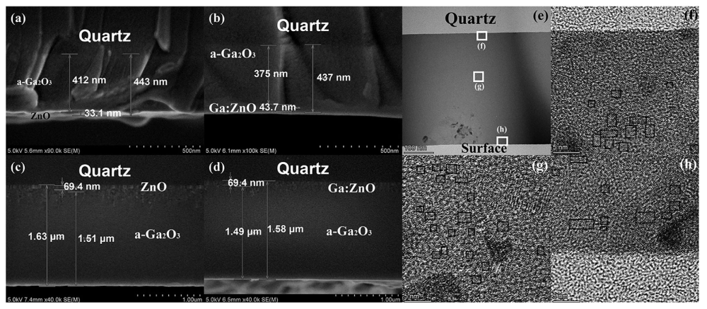
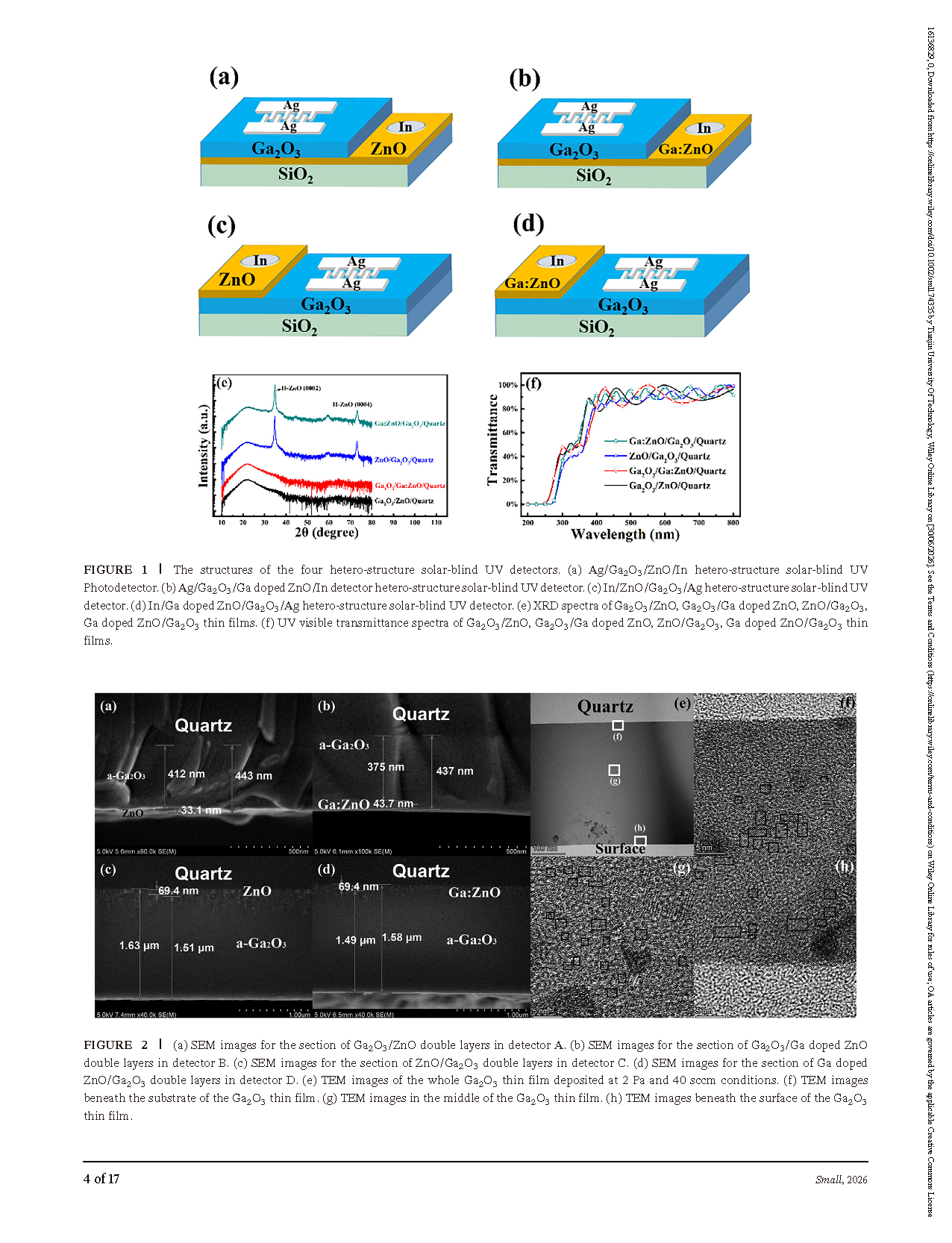
FIGURE 2 (a) SEM images for the section of Ga₂O₃/ZnO double layers in detector A. (b) SEM images for the section of Ga₂O₃/Ga doped ZnO double layers in detector B. (c) SEM images for the section of ZnO/Ga₂O₃ double layers in detector C. (d) SEM images for the section of Ga doped ZnO/Ga₂O₃ double layers in detector D. (e) TEM images of the whole Ga₂O₃ thin film deposited at 2 Pa and 40 sccm conditions. (f) TEM images beneath the substrate of the Ga₂O₃ thin film. (g) TEM images in the middle of the Ga₂O₃ thin film. (h) TEM images beneath the surface of the Ga₂O₃ thin film.
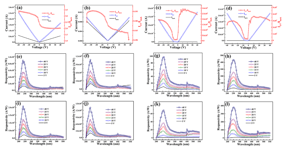
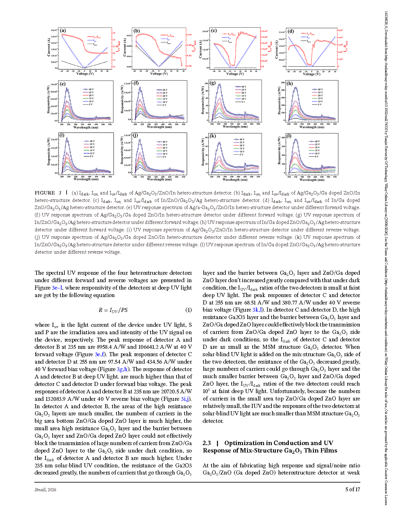
FIGURE 3 (a) Idark, IUV and IUV/Idark of Ag/Ga₂O₃/ZnO/In hetero-structure detector. (b) Idark, IUV and IUV/Idark of Ag/Ga₂O₃/Ga doped ZnO/In hetero-structure detector. (c) Idark, IUV and IUV/Idark of In/ZnO/Ga₂O₃/Ag hetero-structure detector. (d) Idark, IUV and IUV of In/Ga doped ZnO/Ga₂O₃/Ag hetero-structure detector. (e) UV response spectrum of Ag/Ga₂O₃/ZnO/In hetero-structure detector under different forward voltage. (f) UV response spectrum of Ag/Ga₂O₃/Ga doped ZnO/In hetero-structure detector under different forward voltage. (g) UV response spectrum of In/ZnO/Ga₂O₃/Ag hetero-structure detector under different forward voltage. (h) UV response spectrum of In/Ga doped ZnO/Ga₂O₃/Ag hetero-structure detector under different forward voltage. (i) UV response spectrum of Ag/Ga₂O₃/ZnO/In hetero-structure detector under different reverse voltage. (j) UV response spectrum of Ag/Ga₂O₃/Ga doped ZnO/In hetero-structure detector under different reverse voltage. (k) UV response spectrum of In/ZnO/Ga₂O₃/Ag hetero-structure detector under different reverse voltage. (l) UV response spectrum of In/Ga doped ZnO/Ga₂O₃/Ag hetero-structure detector under different reverse voltage.
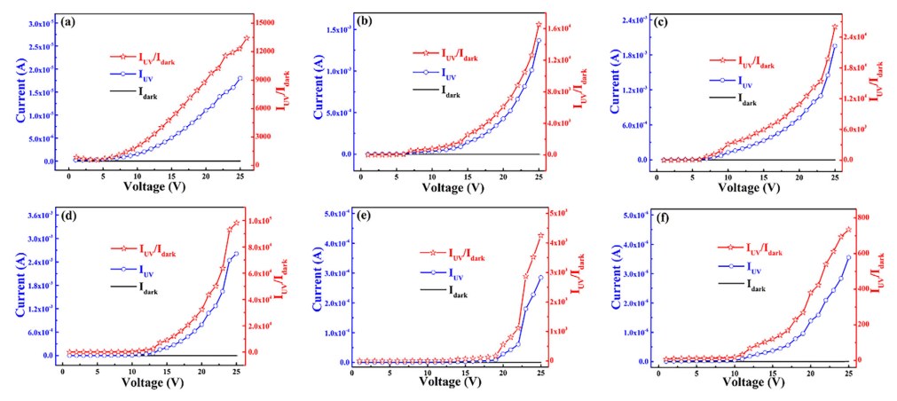
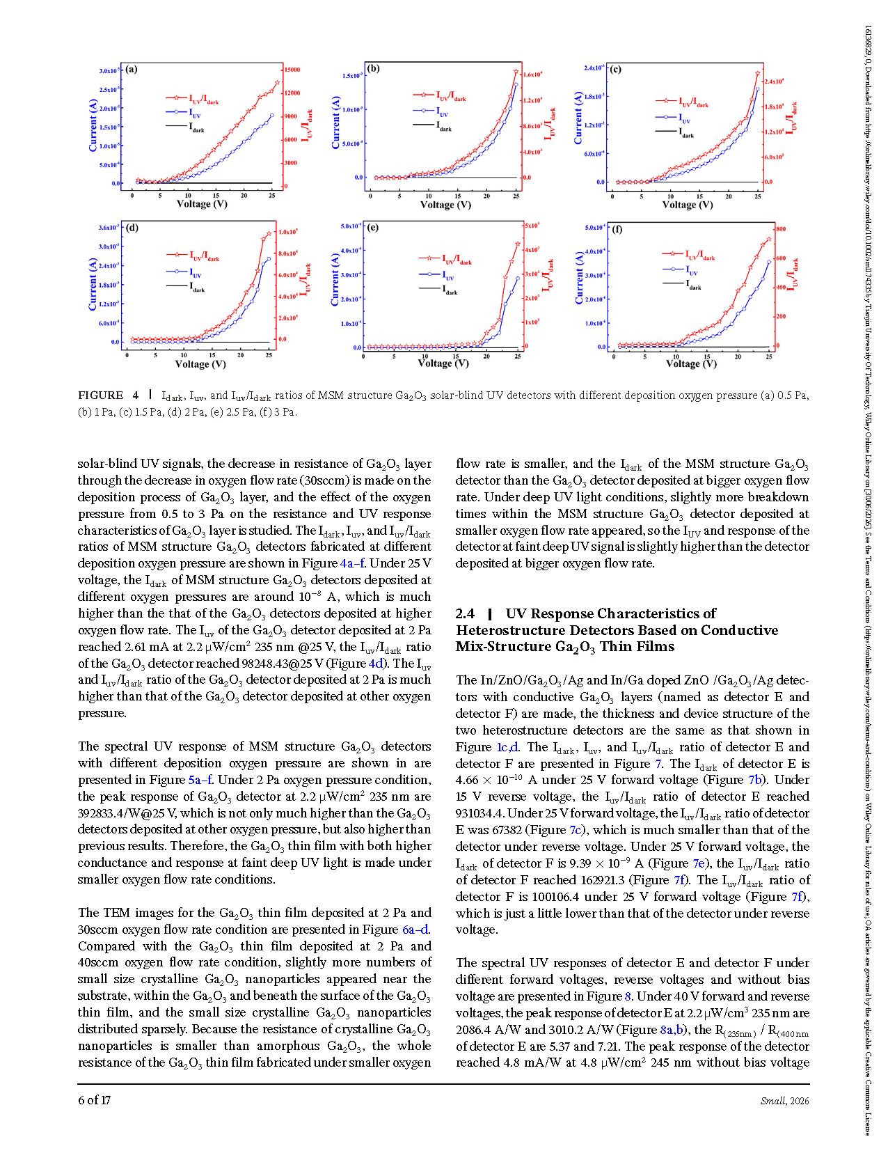
FIGURE 4 Idark, Iuv, and IUV/Idark ratios of MSM structure Ga₂O₃ solar-blind UV detectors with different deposition oxygen pressure (a) 0.5 Pa, (b) 1 Pa, (c) 1.5 Pa, (d) 2 Pa, (e) 2.5 Pa, (f) 3 Pa.
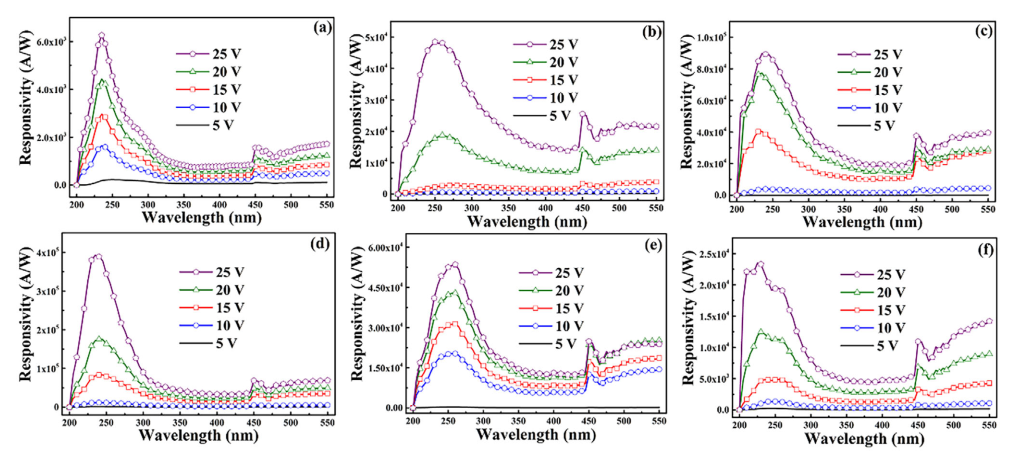
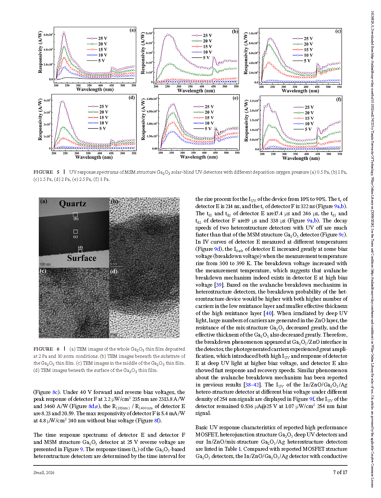
FIGURE 5 UV response spectrums of MSM structure Ga₂O₃ solar-blind UV detectors with different deposition oxygen pressure (a) 0.5 Pa, (b) 1 Pa, (c) 1.5 Pa, (d) 2 Pa, (e) 2.5 Pa, (f) 3 Pa.
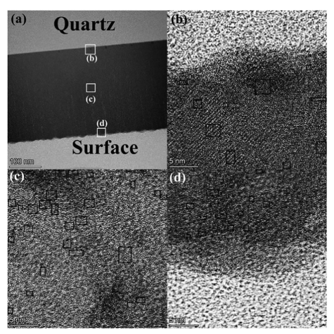
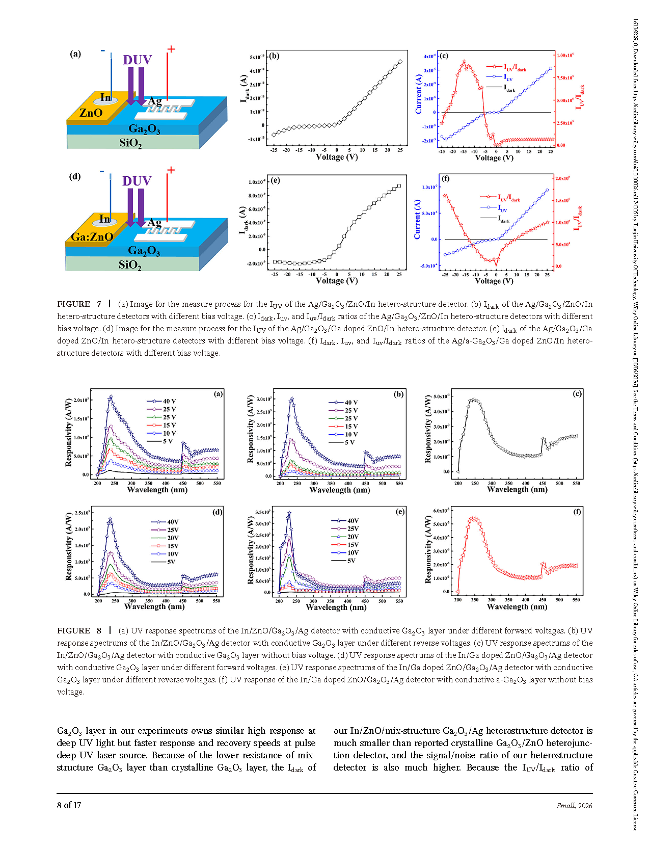
FIGURE 6 (a) TEM images of the whole Ga₂O₃ thin film deposited at 2 Pa and 30 sccm conditions. (b) TEM images beneath the substrate of Ga₂O₃ thin film. (c) TEM images in the middle of the Ga₂O₃ thin film. (d) TEM images beneath the surface of the Ga₂O₃ thin film.
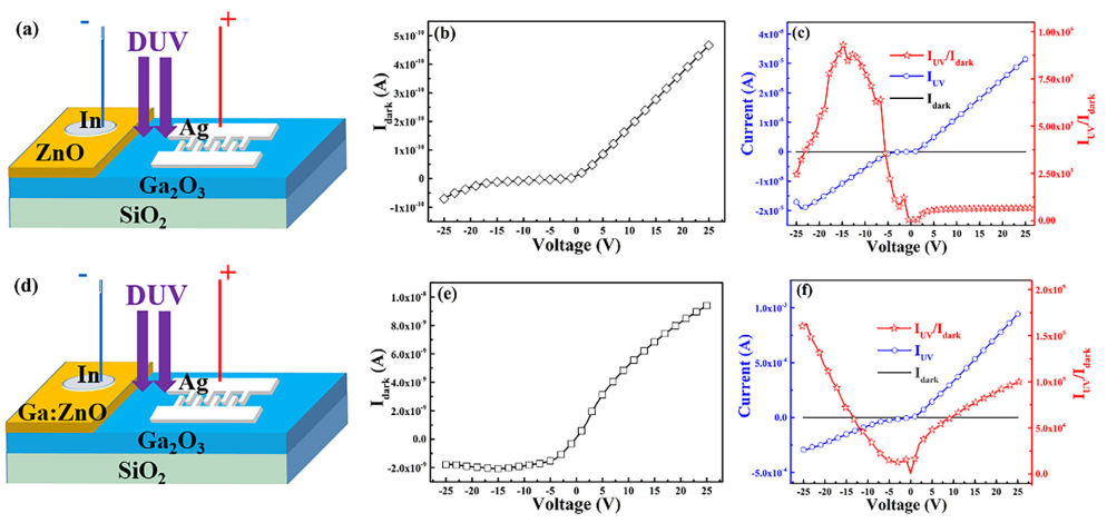
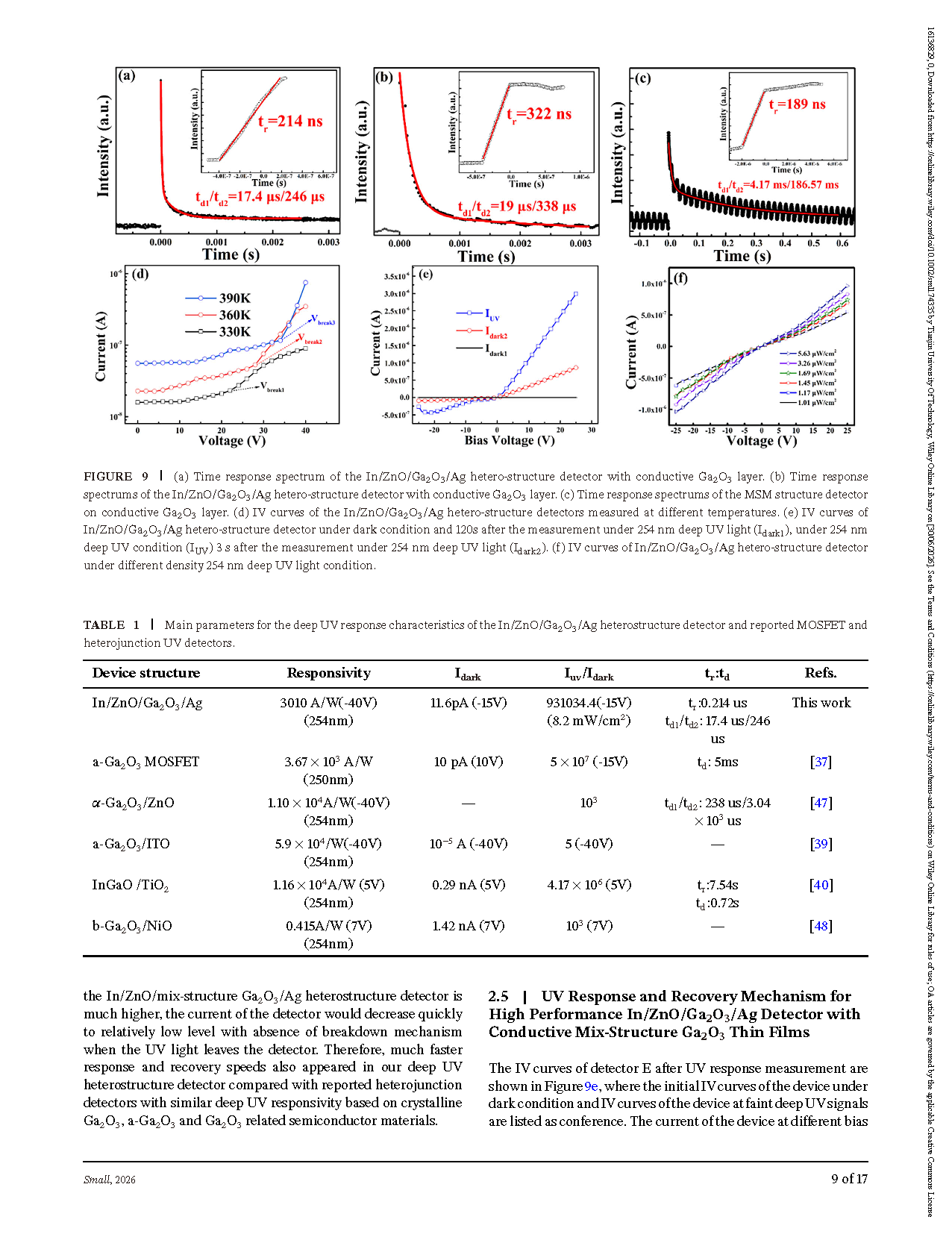
FIGURE 7 (a) Image for the measure process for Ag/Ga₂O₃/ZnO/In hetero-structure detector. (b) Idark, IUV of Ag/Ga₂O₃/ZnO/In hetero-structure detector with different bias voltage. (c) Idark, IUV, and IUV/Idark of Ag/Ga₂O₃/ZnO/In hetero-structure detectors with different bias voltage. (d) Image for the measure process for Ag/Ga₂O₃/Ga doped ZnO/In hetero-structure detector. (e) Idark of Ag/Ga₂O₃/Ga doped ZnO/In hetero-structure detectors with different bias voltage. (f) Idark, IUV, and IUV/Idark of Ag/Ga₂O₃/Ga doped ZnO heterostructure detectors with different bias voltage.
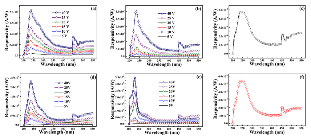
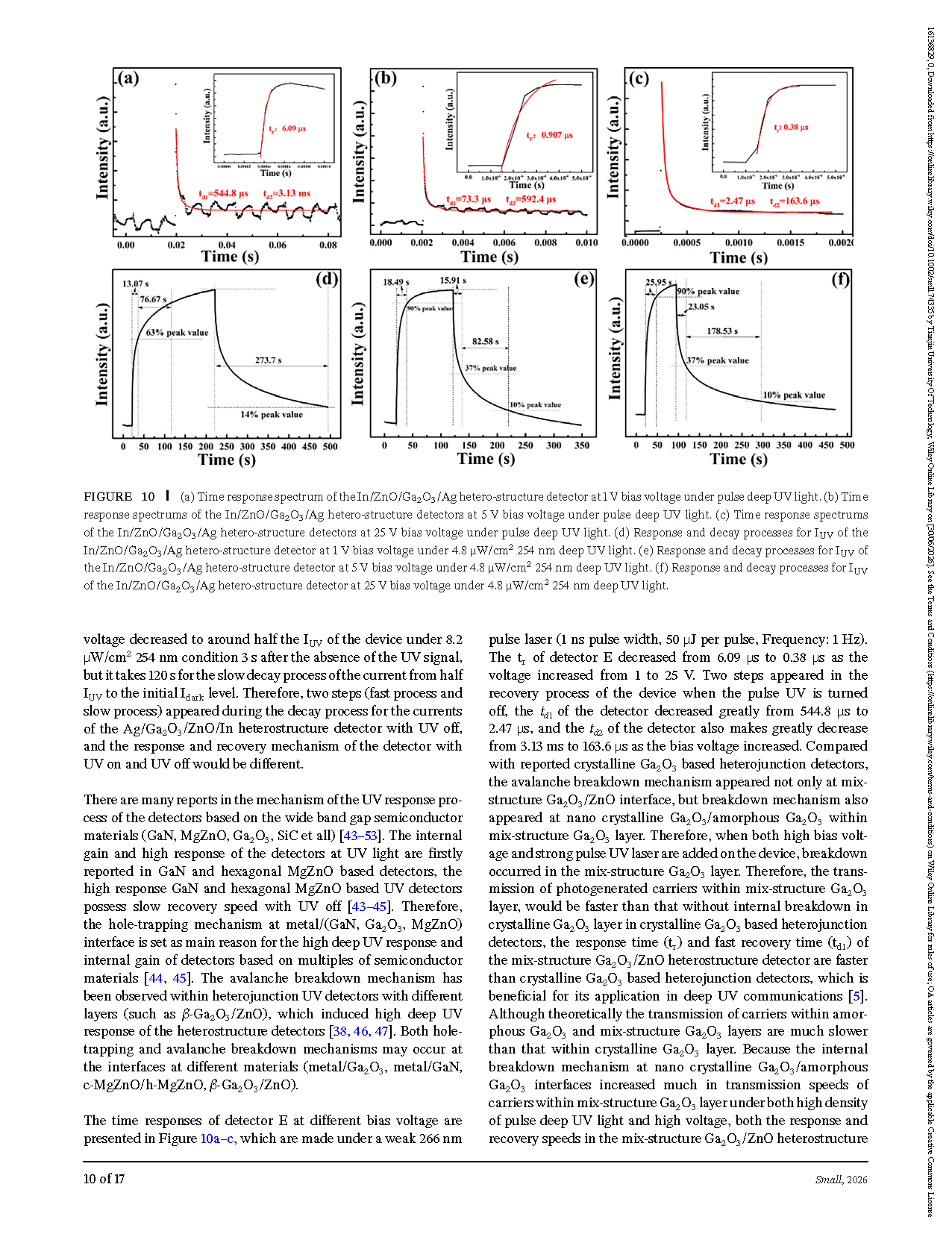
FIGURE 8 (a) UV response spectrums of the In/ZnO/Ga₂O₃/Ag detector with conductive Ga₂O₃ layer under different forward voltages. (b) UV response spectrums of the In/ZnO/Ga₂O₃/Ag detector with conductive Ga₂O₃ layer under different reverse voltages. (c) UV response spectrums of the In/ZnO/Ga₂O₃ detector with conductive Ga₂O₃ layer without bias voltage. (d) UV response spectrums of In/Ga doped ZnO/Ga₂O₃/Ag detector under different forward voltages. (e) UV response spectrums of In/Ga doped ZnO/Ga₂O₃/Ag detector under different reverse voltages. (f) UV response of the In/Ga doped ZnO/Ga₂O₃/Ag detector without bias voltage.
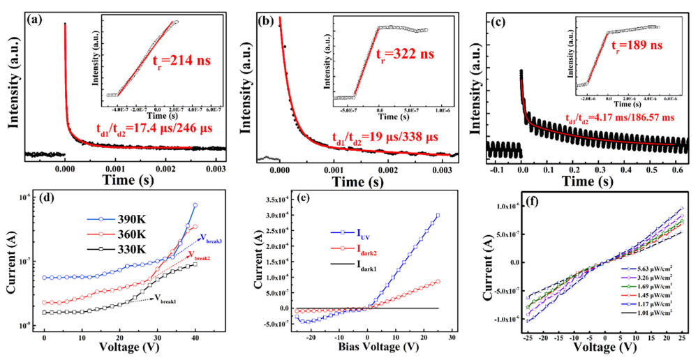
FIGURE 9 (a) Time response spectrum of the In/ZnO/Ga₂O₃/Ag hetero-structure detector with conductive Ga₂O₃ layer. (b) Time response spectrums of the In/ZnO/Ga₂O₃/Ag hetero-structure detector with conductive Ga₂O₃ layer. (c) Time response spectrums of the MSM structure detector on conductive Ga₂O₃ layer. (d) IV curves of the In/ZnO/Ga₂O₃/Ag hetero-structure detectors measured at different temperatures. (e) IV curves of In/ZnO/Ga₂O₃/Ag hetero-structure detector under dark condition and 120s after the measurement under 254 nm deep UV light (Idark1), under 254 nm deep UV condition (IUV) 3 s after the measurement under 254 nm deep UV light (Idark2). (f) IV curves of In/ZnO/Ga₂O₃/Ag hetero-structure detector under different density 254 nm deep UV light condition.
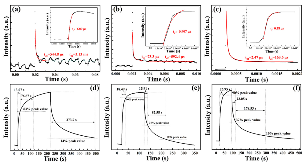
FIGURE 10 (a) Time response spectrum of the In/ZnO/Ga₂O₃/Ag hetero-structure detector at 1 V bias voltage under pulse deep UV light. (b) Time response spectrums of the In/ZnO/Ga₂O₃/Ag hetero-structure detectors at 5 V bias voltage under pulse deep UV light. (c) Time response spectrums of the In/ZnO/Ga₂O₃/Ag hetero-structure detectors at 25 V bias voltage under pulse deep UV light. (d) Response and decay processes for IUV of the In/ZnO/Ga₂O₃/Ag hetero-structure detector at 1 V bias voltage under 4.8 µW/cm² 254 nm deep UV light. (e) Response and decay processes for IUV of the In/ZnO/Ga₂O₃/Ag hetero-structure detector at 5 V bias voltage under 4.8 µW/cm² 254 nm deep UV light. (f) Response and decay processes for IUV of the In/ZnO/Ga₂O₃/Ag hetero-structure detector at 25 V bias voltage under 4.8 µW/cm² 254 nm deep UV light.
DOI:
doi.org/10.1002/smll.74335
Instruction
Official Account

Cooperation
Top
