


Introduction
In the previous issue, we focused on the industrialization of β-Ga₂O₃ homoepitaxy and introduced the two mainstream technology routes, HVPE and MOCVD. HVPE, with its high growth rate, is well suited for forming the thick drift layers required by high-voltage vertical devices, while MOCVD offers excellent control over doping, composition, and interfaces, providing critical support for the fabrication of precisely engineered device functional layers. Together, these two approaches are driving β-Ga₂O₃ epitaxy from laboratory research toward device-level manufacturing.
As epitaxial technologies move toward large-scale application, however, equipment complexity, precursor costs, and process operating costs are becoming increasingly important, alongside crystal quality, growth rate, and doping precision. Particularly for large-area and high-throughput epitaxial manufacturing, how to simplify equipment architecture and lower the barriers to manufacturing while maintaining material quality has emerged as another important direction for the development of Ga₂O₃ epitaxy.
Against this backdrop, mist chemical vapor deposition (Mist-CVD) is attracting growing attention. Unlike conventional vapor-phase epitaxy, which directly delivers gaseous precursors, Mist-CVD first dissolves metal precursors in a liquid solution and then uses ultrasonic atomization to generate fine aerosol droplets. These droplets are transported by a carrier gas into a heated region, where thin-film deposition takes place. Mist-CVD can typically operate at or near atmospheric pressure, eliminating the need for complex vacuum systems. It also offers flexible liquid-phase precursor formulation, a relatively simple equipment architecture, and diverse approaches for controlling crystal phase and doping.
Through the coordinated optimization of liquid-phase precursor chemistry, aerosol transport, and epitaxial growth kinetics, Mist-CVD has demonstrated distinctive advantages in the growth of various Ga₂O₃ phases, including α-, β-, and ε/κ-Ga₂O₃, and is gradually expanding into areas such as homoepitaxy, thick-film growth, and controlled doping.
In this issue, we will begin with the equipment architecture and growth mechanisms of Mist-CVD, before exploring its latest advances in Ga₂O₃ crystal-phase engineering, β-Ga₂O₃ homoepitaxy, liquid-phase doping, and scalable manufacturing.
Issue 11: Mist-CVD and Low-Cost Epitaxy Solutions for Gallium Oxide
Breaking the Vacuum Dependency: How Does Mist-CVD Grow Thin Films?
One of the most distinctive features of Mist-CVD is its use of mist for mass transport.
Conventional MOCVD typically uses highly volatile metal-organic compounds such as TMGa and TEGa as gallium sources. In contrast, Mist-CVD can employ precursors such as GaCl₃ and gallium acetylacetonate (Ga(acac)₃), with water, acidic aqueous solutions, or alcohols selected as solvents depending on the precursor's solubility.
By varying the solution concentration, the precursor supply can be directly adjusted. In practice, however, the effective flux reaching the substrate surface is also influenced by factors such as atomization efficiency, droplet size, carrier-gas flow rate, and losses along the reactor walls [1].
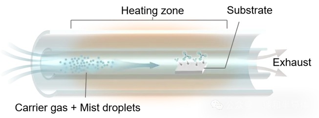
Figure 1. Schematic of the Mist-CVD System Configuration
A typical Mist-CVD system mainly consists of a precursor solution, ultrasonic atomizer, carrier-gas delivery system, and heated reaction zone.
The liquid precursor is first converted into fine aerosol droplets under MHz-range ultrasonic vibration. These droplets are then transported into the reactor by a carrier gas such as N₂, O₂, Ar, or air. As the aerosol enters the high-temperature region, the droplets undergo continuous heating, solvent evaporation, and concentration, while the precursor is further converted into molecules, clusters, or other reactive intermediates, which are ultimately transported toward the vicinity of the substrate.
Therefore, Mist-CVD is far more than simply “spraying droplets onto a wafer and baking them dry.” Instead, it involves a complex sequence of processes, including aerosol formation → droplet transport → solvent evaporation → precursor reactions → surface adsorption → nucleation and crystal growth.
Droplet Transport and Desolvation
Once the droplets enter the heated region, the solvent gradually evaporates and the droplet size continuously decreases. The reaction temperature, carrier-gas flow rate, droplet size, and distance between the substrate and the nozzle can all affect the state of the precursor as it reaches the substrate surface.
This process is critical. If evaporation occurs too early, the precursor may undergo parasitic reactions upstream or on the reactor walls. If the droplets are too large, they may cause non-uniform precursor delivery or even impact the substrate directly. Therefore, Mist-CVD requires control not only over “how much mist is generated,” but also over the physical and chemical state of the precursor reaching the growth surface.
A 2023 study on 2-inch α-Ga₂O₃ growth by Mist-CVD demonstrated the importance of this process. Simply changing the substrate position within the reactor increased the growth rate from 307 nm/h to 1.45 μm/h, highlighting that droplet evaporation and transport are themselves key factors governing deposition efficiency [2].
Leidenfrost Effect
In some Mist-CVD reactor configurations and under specific temperature conditions, researchers have also observed droplet behavior resembling the Leidenfrost effect.
When water-containing microdroplets approach a high-temperature substrate, rapid vaporization at the bottom of the droplets can form a vapor layer that reduces direct contact between the droplets and the solid surface. This can cause the droplets to slide, contract, and redistribute across the substrate.
Such behavior can alter the droplet residence time and the precursor delivery conditions near the substrate surface, potentially affecting the overall deposition process.
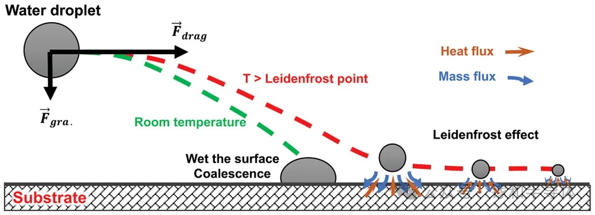
Figure 2. Deposition Behavior of Atomized Droplets on the Substrate Surface at Room and Elevated Temperatures [3]
This phenomenon provides an interesting physical picture for understanding droplet-mediated mass transport in Mist-CVD. In 2021, Ha et al. investigated the motion of water microdroplets near high-temperature substrates and proposed that droplets in Mist-CVD may undergo deposition and sliding driven by the Leidenfrost effect. They further demonstrated the relationship between this mechanism and thin-film deposition behavior through α-Ga₂O₃ epitaxy on 2-inch c-plane sapphire substrates [3].
It is important to note, however, that while the Leidenfrost effect is considered an important mechanism influencing droplet transport and precursor delivery at the substrate surface in Mist-CVD, it is not the sole factor determining epitaxial quality. Droplet evaporation, size evolution, and motion within the reaction zone are also affected by factors including temperature, carrier-gas flow rate, reactor configuration, and substrate position.
Ultimately, stable and effective precursor delivery depends on ensuring that the droplets reach the vicinity of the substrate in an appropriate physical and chemical state. The actual Mist-CVD growth process is therefore governed by the coupled effects of droplet transport, evaporation behavior, and surface chemical reactions.
Surface Chemistry and Epitaxial Crystallization
Studies have shown that when Ga(acac)₃ is used as the precursor, film growth does not simply rely on the complete thermal decomposition of the precursor to generate free Ga species. Previous studies have proposed that the acetylacetonate ligands first interact with surface hydroxyl groups, followed by ligand exchange and the formation of Ga–O bonds, as the acetylacetonate ligands are gradually removed.
Further evidence from isotope tracing and secondary ion mass spectrometry (SIMS) indicates that the oxygen atoms incorporated into the film originate primarily from water in the precursor solution, rather than from external O₂ or the acetylacetonate ligands [4].
This reveals an interesting aspect of Mist-CVD: the solvent is not necessarily just a “transport medium”—it may also participate directly in film formation.
As a result, factors such as the solvent species, solution pH, precursor complexation state, and precursor concentration may all influence the surface reactions and, ultimately, the resulting crystal growth.
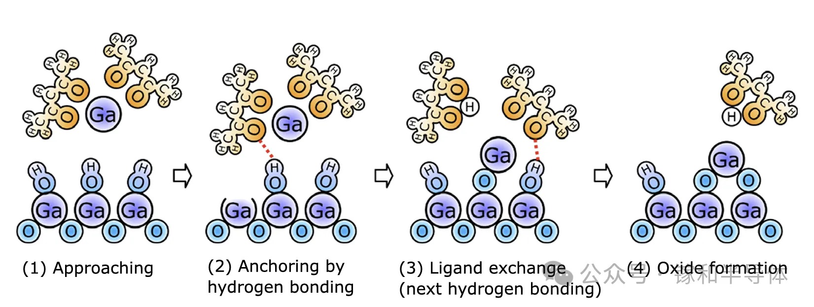
Figure 3. Growth Mechanism of α-Ga₂O₃ by Mist-CVD [4]
Crystal-Phase Engineering
Polymorph-Selective Epitaxy through Multidimensional Process Control
In previous issues, we introduced the rich polymorphic structures of Ga₂O₃. At present, the thermodynamically stable β phase remains the primary focus of industrial development, while metastable phases such as α- and ε/κ-Ga₂O₃ have also attracted considerable attention due to their distinctive physical properties.
Breaking beyond the growth window of a single crystal phase and enabling the controlled growth of different Ga₂O₃ polymorphs is therefore an important challenge for epitaxial technology. In this regard, Mist-CVD has demonstrated notable capabilities for crystal-phase control.
Built around solution-based precursor formulation, ultrasonic atomization, and aerosol transport, Mist-CVD enables researchers to tune the growth of different crystal phases by selecting appropriate substrates and buffer layers and adjusting parameters such as growth temperature, precursor supply, oxygen partial pressure, and reactor pressure. These variables can alter the interfacial stability, supersaturation, and competition among nucleation processes associated with different polymorphs.
To date, the Mist-CVD technology platform has enabled the epitaxial growth of multiple Ga₂O₃ polymorphs, including α-, β-, and ε/κ-Ga₂O₃ [5].
A Mild Low-Temperature Kinetic Growth Window
Unlike conventional vapor-phase deposition techniques, Mist-CVD uses atomized droplets as the precursor source, enabling precursor decomposition and crystallization within a relatively mild temperature range of 400°C to 600°C.
This low-temperature environment can effectively shift the epitaxial growth process from being thermodynamically dominated to kinetically dominated, helping suppress the transformation of metastable phases into the thermodynamically stable β phase.
Exceptional Process Flexibility
Mist-CVD gives operators a high degree of flexibility in process control. By simply fine-tuning the precursor-solution concentration, adjusting the carrier-gas flow rate to control the deposition rate, or precisely controlling the temperature of the heating zone, different crystal phases can be selectively grown within the same equipment platform. The approach can even enable the design of complex phase-composition gradients.
In recent years, Mist-CVD has continued to advance in the epitaxial growth of Ga₂O₃ polymorphs, gradually expanding its capabilities to cover different phases, including α-, β-, and ε/κ-Ga₂O₃. Meanwhile, continued optimization has improved key growth metrics such as phase purity, crystalline quality, and growth rate.
Doping Flexibility
From Liquid-Phase Mixing to Electrical Property Control
For β-Ga₂O₃, considerable progress has been made in donor doping with elements such as Si, Sn, and Ge. However, challenges remain in controlling low carrier concentrations, compensating for background impurities, and achieving stable p-type doping.
Compared with approaches such as MOCVD, which rely on volatile dopant sources and dedicated gas-delivery systems, Mist-CVD can directly add soluble dopant precursors to the Ga-source solution. By adjusting the ratio of the dopant precursor to the Ga precursor, the nominal dopant concentration can be controlled, simplifying the introduction and switching of dopant sources. To date, dopants such as SnCl₂, Si-containing organic precursors, and GeI₄ have been used for Ga₂O₃ doping by Mist-CVD [6–8].
Taking Si-doped β-Ga₂O₃ as an example, varying the Si concentration in the precursor solution enabled the room-temperature carrier concentration to be tuned from 3.85 × 10¹⁸ to 2.58 × 10²⁰ cm⁻³. The series of samples exhibited RMS surface roughness below 0.5 nm, while the lowest FWHM of the (020) rocking curve was approximately 40 arcsec. The highest electrical conductivity reached 2368 S/cm, corresponding to a carrier concentration of 2.58 × 10²⁰ cm⁻³ and a mobility of 57.2 cm²/V·s [7].
These results demonstrate that Mist-CVD can enable high-concentration n-type doping of β-Ga₂O₃ while achieving relatively high electrical conductivity in the resulting films.
Research Progress
Based on the existing body of research, α-Ga₂O₃ is one of the earliest Ga₂O₃ polymorphs to be grown epitaxially by Mist-CVD and has accumulated the most systematic research to date. Benefiting from the similar corundum crystal structure of α-Ga₂O₃ and c-plane sapphire, researchers have achieved 2-inch wafer-scale heteroepitaxial growth of α-Ga₂O₃ on c-plane sapphire substrates.
By optimizing the growth temperature and the relative position between the substrate and the mist outlet, the maximum film growth rate reached 1.45 μm/h. At 540°C, the FWHM of the X-ray rocking curve for the (0006) reflection was as low as 0.023° [2], demonstrating the capability of Mist-CVD to produce large-area α-Ga₂O₃ films with high crystalline quality.
Building on this work, researchers further investigated the evolution of the structural and optical properties of α-Ga₂O₃ films over a thickness range from 17 nm to 4.8 μm. At a steady-state growth rate of approximately 400 nm/h, the films maintained α-phase epitaxy throughout the growth process while exhibiting pronounced thickness-dependent characteristics.
By correlating the evolution of surface morphology, crystalline quality, stress state, and optical properties across different film thicknesses, the researchers proposed a thickness-driven three-stage growth model. This model provides experimental evidence for understanding the evolution of α-Ga₂O₃ from initial nucleation and island formation to the development of continuous thick films [9].
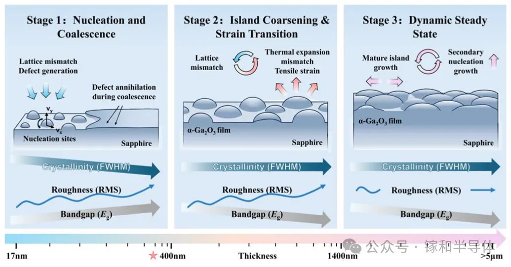
Figure 4. Three-Stage Growth Model of Mist-CVD Heteroepitaxial α-Ga₂O₃ Films with Increasing Thickness [9]
For the thermodynamically stable β-Ga₂O₃ phase, Mist-CVD research has gradually expanded from heteroepitaxy on sapphire to micrometer-scale thick-film growth on homoepitaxial single-crystal substrates.
For heteroepitaxial growth, the substantial structural mismatch between β-Ga₂O₃ and sapphire can readily lead to multi-orientation nucleation, rotational domains, and interfacial defects. To address these issues, researchers introduced a NiO buffer layer on c-plane sapphire substrates.
Based on the epitaxial matching relationship adopted in the study, the lattice mismatch between NiO and β-Ga₂O₃ is approximately 0.46%, significantly lower than the approximately 6.6% mismatch between β-Ga₂O₃ and sapphire. With the introduction of the buffer layer, the FWHM of the rocking curve for the β-Ga₂O₃ film decreased from 0.726° to 0.514°, while the RMS surface roughness decreased from 7.47 nm to 3.34 nm [10].
These results indicate that the NiO buffer layer can improve, to some extent, the heteroepitaxial nucleation and film coalescence processes.
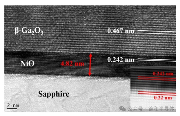
Figure 5. NiO Buffer Layer-Assisted Heteroepitaxial Growth of β-Ga₂O₃ by Mist-CVD [10]
On the other hand, Mist-CVD has also made steady progress in β-Ga₂O₃ homoepitaxy. Early studies identified a suitable growth window of approximately 700–800°C on (010) substrates [11]. Subsequently, by increasing the concentration of the GaCl₃ precursor, researchers achieved a growth rate of 3.2 μm/h at 750°C, while obtaining a smooth, single-oriented film [12].
More recently, a hydrochloric acid-assisted process increased the growth rate of (001) homoepitaxy by approximately 4.8×, while also improving the surface morphology of samples with comparable thicknesses [13]. Using gallium acetylacetonate (Ga(acac)₃) as the precursor, researchers also achieved thick-film homoepitaxial growth at approximately 2 μm/h on (-201) substrates [14].
Taken together, these results show that Mist-CVD has been demonstrated across multiple β-Ga₂O₃ orientations, including (010), (001), and (-201), highlighting its potential for the high-throughput growth of micrometer-scale β-Ga₂O₃ epitaxial layers.
ε/κ-Ga₂O₃: Another Key Direction in Crystal-Phase Engineering
ε/κ-Ga₂O₃ represents another important research direction in Mist-CVD-based crystal-phase engineering in recent years. By synergistically tuning the growth temperature and oxygen flow rate, researchers achieved a transition from an α–ε mixed phase to single-phase ε-Ga₂O₃, with an X-ray rocking-curve FWHM as low as 0.073° and an RMS surface roughness of approximately 0.75 nm [15].
A research team in China further built on an α-Ga₂O₃ Mist-CVD platform and obtained single-phase ε-Ga₂O₃ on c-plane sapphire by optimizing the oxygen flow rate, achieving a maximum growth rate of 3 μm/h [16].
In addition, Sn-assisted low-pressure Mist-CVD has been used to produce single-phase ε-Ga₂O₃ with an FWHM of approximately 0.08° for the (004) rocking curve and an RMS surface roughness of approximately 1.51 nm, further expanding the available approaches for stabilizing the ε/κ phase [17].
Industrialization: Epitaxial Processes
Engineering Bottlenecks and Solutions for Scale-Up
With its inherent advantages of vacuum-free operation and low cost, Mist-CVD has demonstrated its technical feasibility at the laboratory scale. However, moving from the laboratory to the wafer fab still presents a series of engineering challenges that must be addressed for large-scale manufacturing.
Uniformity Challenges
In conventional hot-wall Mist-CVD systems, atomized droplets are transported in a horizontal laminar flow by the carrier gas. As the precursor is continuously consumed along the flow direction, while gravity-induced droplet settling further affects precursor transport, large-area wafers can readily suffer from non-uniform film thickness and dopant concentration between the center and edge, as well as between the upstream and downstream regions.
To overcome this bottleneck, the industry needs to accelerate the development of microchannel-based flow designs and vertical showerhead architectures, enabling more uniform precursor delivery across large-area substrates.
The Trade-Off Between Growth Rate and Precursor Utilization
High-power electronic devices often require high-purity drift layers with thicknesses exceeding 10 μm. Although Mist-CVD can currently achieve growth rates of several micrometers per hour, the present rate remains insufficient for high-volume production of thick epitaxial layers.
At the same time, a substantial amount of unreacted mist is discharged with the exhaust gas, reducing precursor utilization efficiency. Addressing this bottleneck will require further increasing the mist generation capacity while separating the droplet transport zone from the high-temperature crystallization zone. This can help prevent premature vaporization and gas-phase parasitic reactions before the droplets reach the substrate, thereby maximizing the conversion of the precursor into high-quality epitaxial layers.
Summary
With its non-vacuum, near-atmospheric-pressure processing, high degree of freedom in crystal-phase control, and highly simplified liquid-phase doping process, Mist-CVD is emerging as a potentially transformative technology for Ga₂O₃ epitaxial growth. At a fundamental process level, it breaks the conventional reliance of epitaxial manufacturing on high-vacuum environments, significantly reduces equipment depreciation and maintenance costs, and opens a promising new route for overcoming the thermodynamic limitations associated with the growth of metastable phases.
To date, Mist-CVD has demonstrated wafer-scale heteroepitaxy of α-Ga₂O₃, rapid homoepitaxy and micrometer-scale thick-film growth of β-Ga₂O₃, as well as single-phase growth of ε/κ-Ga₂O₃, highlighting its versatility for the epitaxial growth of different Ga₂O₃ polymorphs. The use of liquid-phase precursor formulations also makes it more convenient to introduce and adjust the ratios of dopant precursors such as Si, Sn, and Ge, providing a flexible approach to controlling carrier concentration and the electrical conductivity of epitaxial films. Particularly for metastable-phase growth, Mist-CVD can expand the epitaxial growth windows of α- and ε/κ-Ga₂O₃ through substrate or buffer-layer-induced phase stabilization and kinetic control of the growth process.
However, it is important to note that Mist-CVD remains at the transition stage from laboratory-scale research to large-scale industrial application. Further development is still needed in areas including large-area uniformity, background impurity control, thick-film quality, and long-term operational stability.
References:
[1] Mater. Today Phys., 2024, 49: 101604.
[2] J. Semicond., 2023, 44: 062803.
[3] Adv. Mater. Interfaces, 2021, 8: 2001895.
[4] Appl. Phys. Lett., 2020, 117: 052106.
[5] J. Appl. Phys., 2022, 131: 090902.
[6] Phys. Status Solidi A, 2020, 217: 1900632.
[7] AIP Adv., 2024, 14: 015040.
[8] Jpn. J. Appl. Phys., 2023, 62: SF1016.
[9] Ceram. Int., 2026, in press.
[10] Vacuum, 2025, 231: 113777.
[11] Jpn. J. Appl. Phys., 2016, 55: 1202B8.
[12] Mater. Sci. Semicond. Process., 2021, 128: 105732.
[13] AIP Adv., 2024, 14: 085309.
[14] Mater. Today Commun., 2024, 41: 110970.
[15] J. Alloys Compd., 2025, 1046: 184847.
[16] J. Chin. Ceram. Soc., 2024, 52: 373–380.
[17] Appl. Phys. Lett., 2025, 127: 102109.
Instruction
Official Account

Cooperation
Top
