



In August 2026, experts, researchers, corporate representatives, and industry professionals from across the global gallium oxide community gathered in Maryland, USA, for the 6th International Workshop on Gallium Oxide and Related Materials (IWGO-6).
From crystal growth and epitaxy to device development and industrialization, the five-day conference brought together the latest advances from different regions around the world, offering a clear view of how gallium oxide is gradually moving beyond cutting-edge laboratory research toward a more defined path to commercialization.
But what a conference leaves behind is far more than presentations, posters, and data.
At IWGO-6, we spoke with experts, researchers, and industry representatives from different countries and regions, hearing their perspectives on technological progress, industrialization, and the future of the industry. These voices from the front lines of the field may offer a deeper understanding than technical performance metrics alone: Where does the global Ga₂O₃ industry stand today, and where is it heading next?
We have captured these perspectives as a snapshot of an industry entering its next stage of development.
Let’s start from IWGO-6 and hear the voices of the global Ga₂O₃ industry.
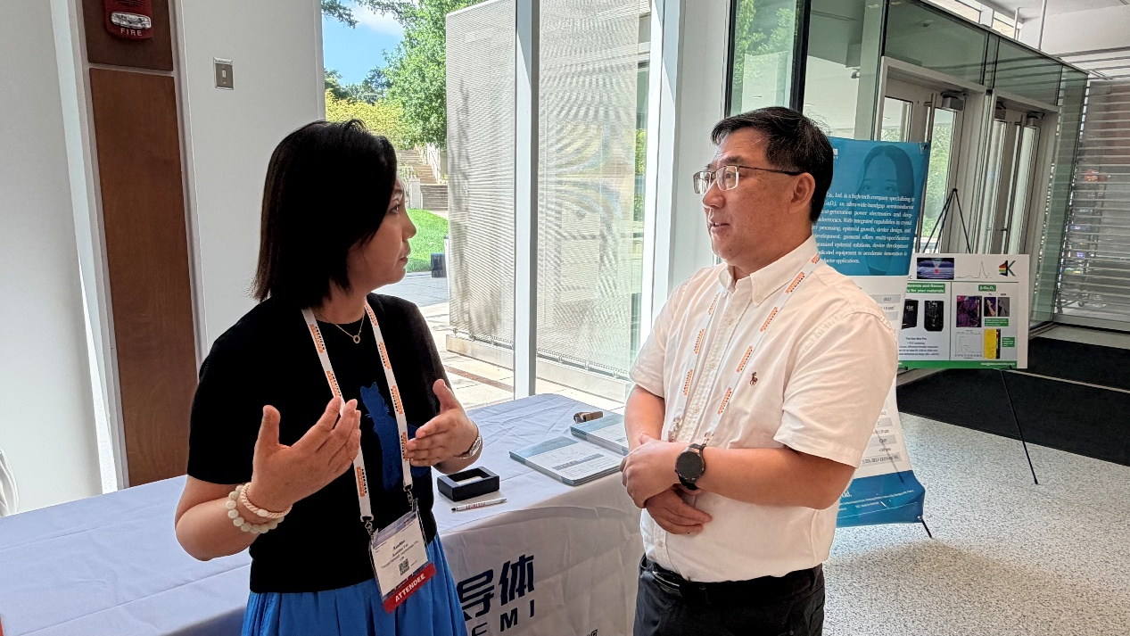
In this issue, we speak with Tang Weihua, Chairman of Suzhou GAO Semiconductor, who shares his observations and insights into the future development of the Ga₂O₃ industry from multiple perspectives, including materials technology, supply-chain collaboration, and commercialization.

How Do You View the Overall IWGO-6 Conference and the Development of International Peers?
The conference brought together many of the latest advances in Ga₂O₃ research worldwide. My most direct impression is that global research on Ga₂O₃ is still advancing rapidly, but the way researchers approach the field has changed. In the past, discussions focused more on material properties and individual device performance metrics. Today, researchers are working across the entire value chain, from materials and different crystal-growth approaches to device validation. Research is becoming not only more in-depth, but also more interconnected across the upstream and downstream sectors, with industrialization now receiving much greater attention.
Looking at developments across different countries and regions, Japan continues to maintain strong advantages in large-size substrates and diverse crystal-growth technologies. The conference showcased the latest progress, including 6-inch substrates grown by the EFG method. Japanese research institutes and companies are also continuing to explore different crystal-growth approaches, including the vertical Bridgman method and the directional solidification (DG) method, while developing new application areas such as process-cost reduction and optical microcavities. However, some of these cutting-edge technologies remain primarily at the stage of process validation or sample demonstration, and there is still a gap before they can evolve into mature products with stable mass-production capabilities.
The United States is also actively advancing research on Ga₂O₃ crystal growth, engineering simulation, and device technologies, although some results remain in the stages of engineering development and commercialization validation. Further accumulation of experience and data will be needed before these technologies can achieve large-scale deployment.
Therefore, I tend to view the industry’s current stage as a shift from “whether it can be done” to “whether it can be done reliably.” Basic demonstrations from materials to devices have reached a level of maturity sufficient for further application exploration. The next challenge is to improve product consistency, manufacturing costs, and application validation—to turn laboratory results into products that customers are willing to use over the long term.
What Are China’s Strengths in Developing the Ga₂O₃ Industry, and What Areas Still Need Improvement?
China’s key advantage is its relatively complete industrial chain. Teams are already working across single-crystal growth, substrates, epitaxy, devices, equipment, and applications. The country also has a solid foundation in manufacturing infrastructure, engineering talent, and supply-chain responsiveness. As application demand gradually expands, this level of industrial completeness could translate relatively quickly into advantages in iteration speed and manufacturing costs.
Taking GAO Semiconductor as an example, we currently regard the EFG method as a core technology route for the industrialization of β-Ga₂O₃ single crystals and substrates. We are also optimizing crystal growth, crystal orientation control, directional cutting, grinding and polishing, and inspection and evaluation as an integrated process chain. In terms of size and crystal orientation, the company has achieved stable supply of high-quality, twin-free Ga₂O₃ substrates ranging from 2 to 6 inches in the (100) orientation and 2 to 4 inches in the (001) orientation, and has completed the development of 6-inch (001) Ga₂O₃ crystals. We particularly emphasize the industrialization of (001) substrates, because for device and epitaxy customers, what matters is not just wafer diameter, but also twin-free crystal control, electrical uniformity, processing-induced damage, and compatibility with epitaxial growth. The company can also provide substrates with different electrical characteristics according to application requirements, including unintentionally doped, Fe-doped semi-insulating, and Sn-doped conductive substrates.
The shortcomings are also quite clear. Much of the current research still focuses on individual performance metrics, and there remains a gap between the best results reported in papers and the batch-to-batch consistency required for commercial products. For applications such as power devices and detectors, more long-term reliability data and system-level validation are needed. A single test result is not enough to demonstrate commercial viability.
In addition, upstream and downstream collaboration still needs to become more closely integrated. Many issues spanning crystal growth, epitaxy, devices, and specialized equipment need to be addressed jointly. For example, the stability of the thermal field and control of volatile species in high-temperature crystal-growth equipment, residue management in epitaxy systems, and the impact of substrate defects on device performance all require material, equipment, and device companies to connect and share their data at an earlier stage.
Given the Current Development Stage of the Ga₂O₃ Industry, How Do You View Private‑Sector Capital Participation and the Path Toward Sustainable Growth?
I do not think that large-scale capital investment is necessarily better the earlier or the greater it is. The key is to match capital deployment with the maturity of the industry. Ga₂O₃ is still in a period of technological iteration and engineering validation, with many areas requiring further data accumulation and process refinement. If companies start projecting million-wafer production capacity and extreme cost targets based on the assumptions of a mature semiconductor industry at this stage, they may be pushed into an inappropriate pace of development.
What the industry needs more at this stage is “patient capital.” Capital should prioritize projects that can address gaps in the industrial chain, develop stable products, and complete validation in real-world application scenarios, rather than simply chasing records in wafer size or individual performance metrics. Government policies and industry organizations can also play a role by helping establish standards, testing methodologies, and demonstration applications as quickly as possible.
Industry–academia–research collaboration should also shift from project-based cooperation toward joint R&D. Companies have a clearer understanding of engineering challenges, while universities and research institutions have strengths in mechanism studies, testing, and analysis. If both sides can jointly define problems, share data, and continuously iterate, the path from research results to practical applications can be significantly accelerated.
Larger wafer sizes are certainly an important direction, but producing a large-size sample and achieving stable mass production are two different things. At the current stage, yield, batch-to-batch consistency, long-term reliability, and cost control should be evaluated together. Only when these fundamentals are firmly established can the advantage of larger wafer sizes truly translate into a commercial advantage.
Looking Ahead, What Are Your Suggestions for Improving Academic Exchange and Advancing Technology Development in the Ga₂O₃ Industry?
Beyond large international conferences, I hope the industry can create more small-scale, problem-oriented opportunities for technical exchange. For example, how different crystal-growth methods can balance crystal quality and cost, how to control residues in epitaxy equipment, and how doping and defects affect electrical uniformity are all issues that are difficult to address thoroughly in a single keynote presentation. They are better discussed when teams from materials, equipment, and device companies sit together and openly share both their data and their experiences with failures.
We should certainly keep track of new developments overseas, but we do not need to immediately follow every emerging approach. Every technology route has its own applicable boundaries. Ultimately, the focus should return to the product: Can it be reproduced consistently? Can it be supplied reliably over time? And can its cost be accepted by the market? China already has a relatively complete industrial foundation. The next step is to develop distinctive strengths along different technology routes and deepen collaboration across the industrial chain around real-world applications.
Products and Technological Capabilities of Suzhou GAO Semiconducto

Suzhou GAO Semiconductor Co., Ltd. has long focused on β-Ga₂O₃ single-crystal growth, precision substrate processing, and epitaxial technology development. The company uses the EFG method as its core crystal-growth route while also conducting validation of other technology approaches. It has established an integrated technology chain covering crystal growth, crystal orientation and electrical-property control, directional cutting, grinding and polishing, surface inspection, and epitaxial validation. The company provides single-crystal substrates, homoepitaxial/heteroepitaxial wafers, and customized material services for universities, research institutes, and epitaxy and device companies.
At present, the company can stably supply high-quality, twin-free Ga₂O₃ substrates from 2 to 6 inches in the (100) orientation and from 2 to 4 inches in the (001) orientation. Sample development of 6-inch (001) Ga₂O₃ single crystals has also been completed. Its product portfolio includes unintentionally doped, Fe-doped semi-insulating, and Sn-doped conductive substrates, with customization available according to crystal orientation, wafer size, epitaxial thickness, and doping requirements. Rather than simply pursuing wafer-size records, the company focuses on continuously improving crystal integrity, electrical uniformity, surface quality, and batch-to-batch consistency as wafer sizes scale up.
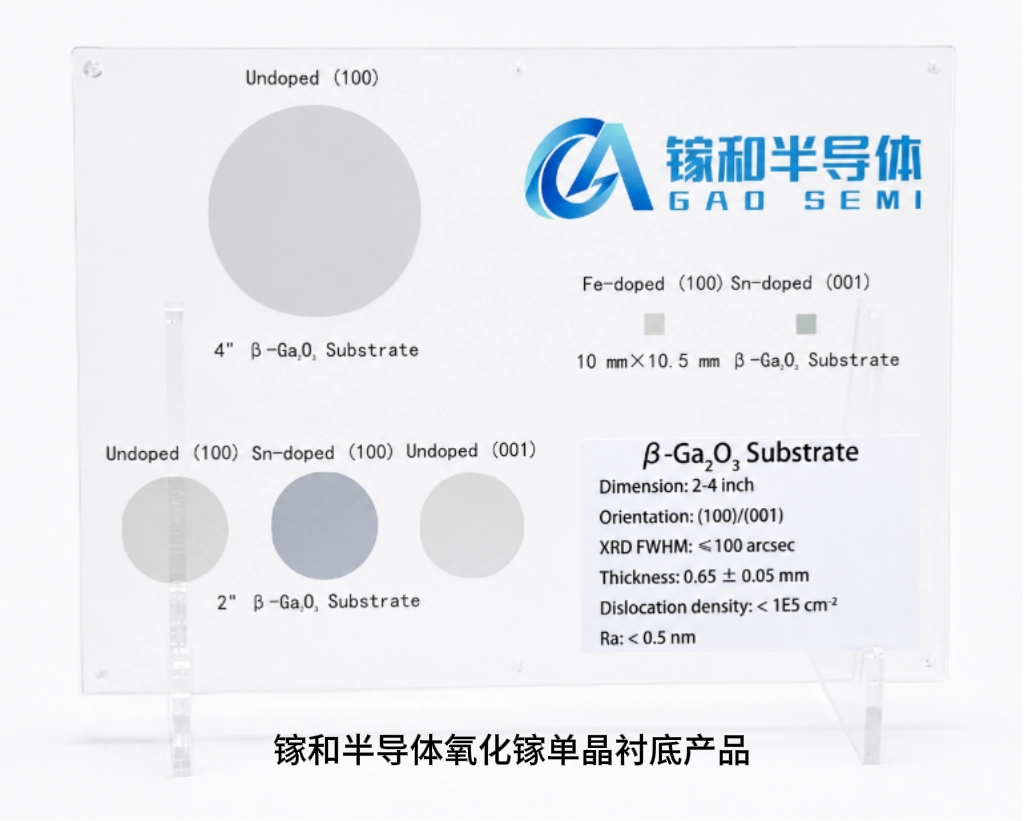
Gallium Oxide Single Crystal Substrate Products of Suzhou GAO Semiconductor Co., Ltd.
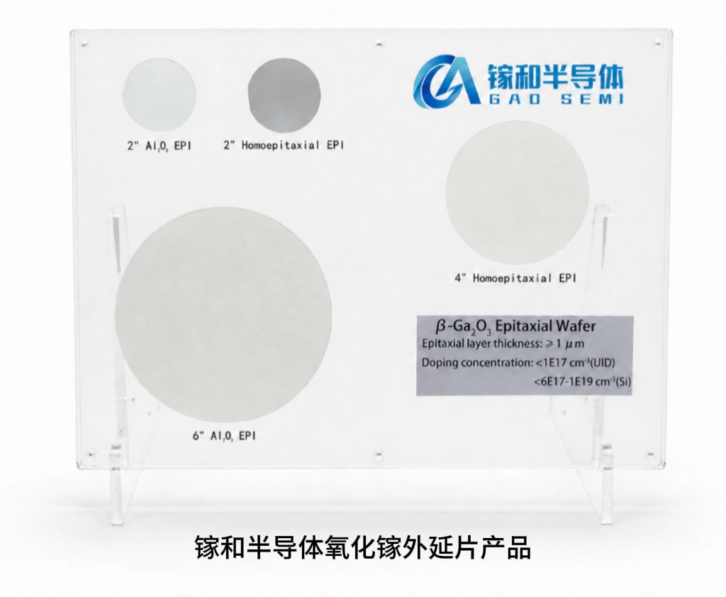
Gallium Oxide Epitaxial Wafer Products of Suzhou GAO Semiconductor Co., Ltd.
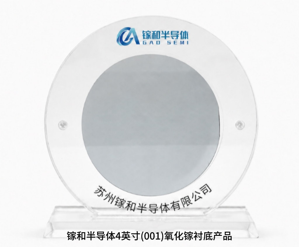
4-inch (001) Gallium Oxide Substrate Products of Suzhou GAO Semiconductor Co., Ltd.
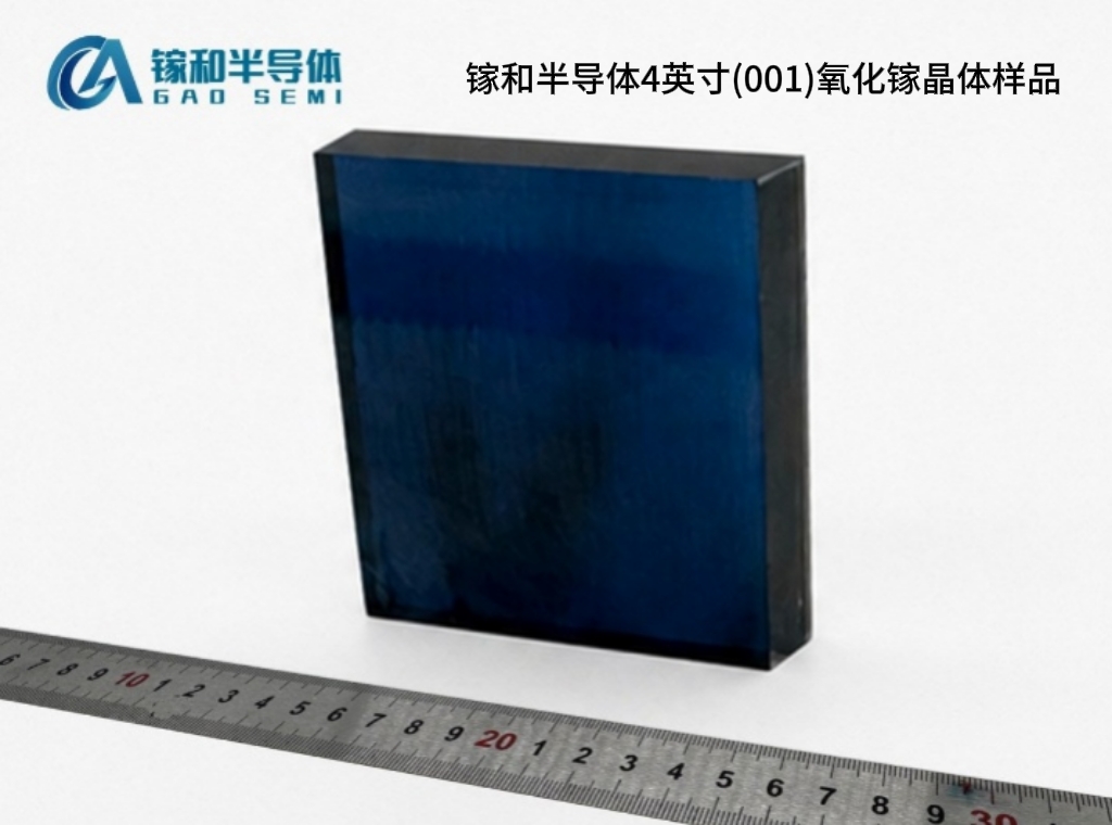
4-inch (001) Gallium Oxide Crystal Samples of Suzhou GAO Semiconductor Co., Ltd.
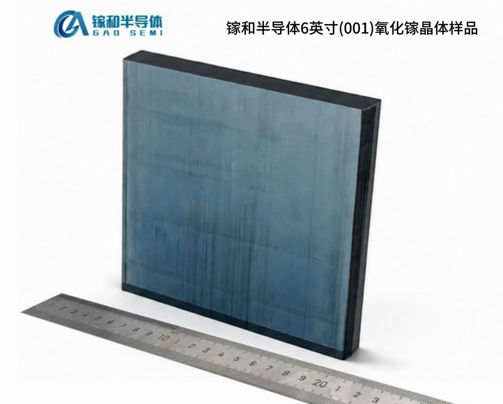
6-inch (001) Gallium Oxide Crystal Samples of Suzhou GAO Semiconductor Co., Ltd.
Instruction
Official Account

Cooperation
Top
