


A New Semester Begins, and the Time for Research and Innovation Is Now
To support universities, research institutes, and enterprise R&D teams in conducting gallium oxide materials research, process validation, and device development, Fujia Gallium is launching a “Back-to-School Season Mega Promotion” from September 1 to 30, 2026, offering more attractive product solutions to help research projects get off to an efficient start.
01 Double Discounts to Empower Scientific Innovation
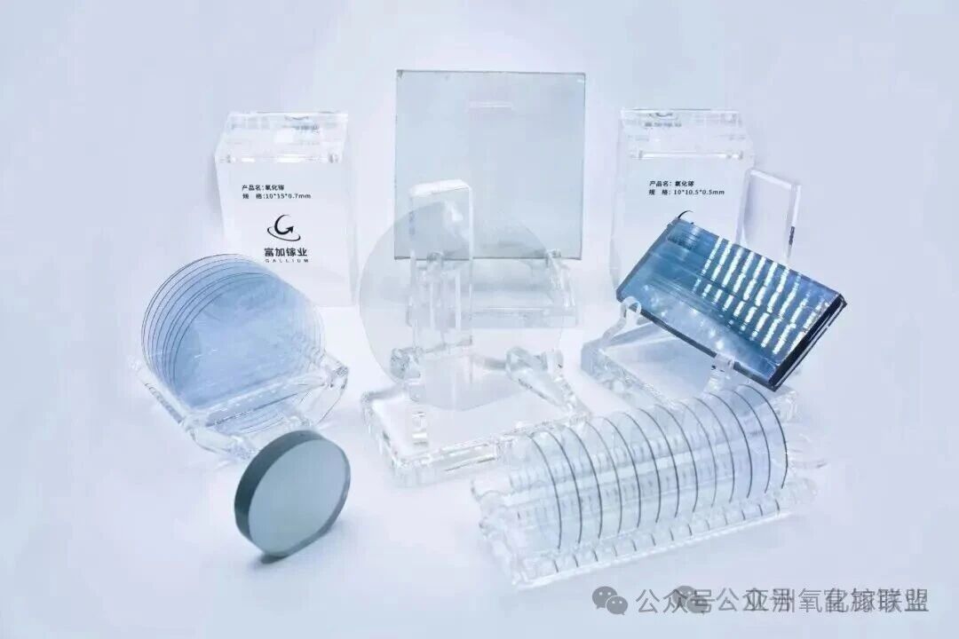
During the promotion, research-grade gallium oxide wafers will be available at 60% off, suitable for research scenarios such as materials characterization, epitaxy experiments, and device process exploration. For prime-grade gallium oxide wafers, a “buy two, get one free” offer will be provided, supporting R&D tasks with higher requirements for material quality and experimental continuity. Through this campaign, Fujia Gallium hopes to further reduce the costs of preliminary trials and sample validation, enabling more research teams to conveniently use high-quality gallium oxide materials.
02 Product Introduction
Gallium Oxide Single-Crystal Substrates
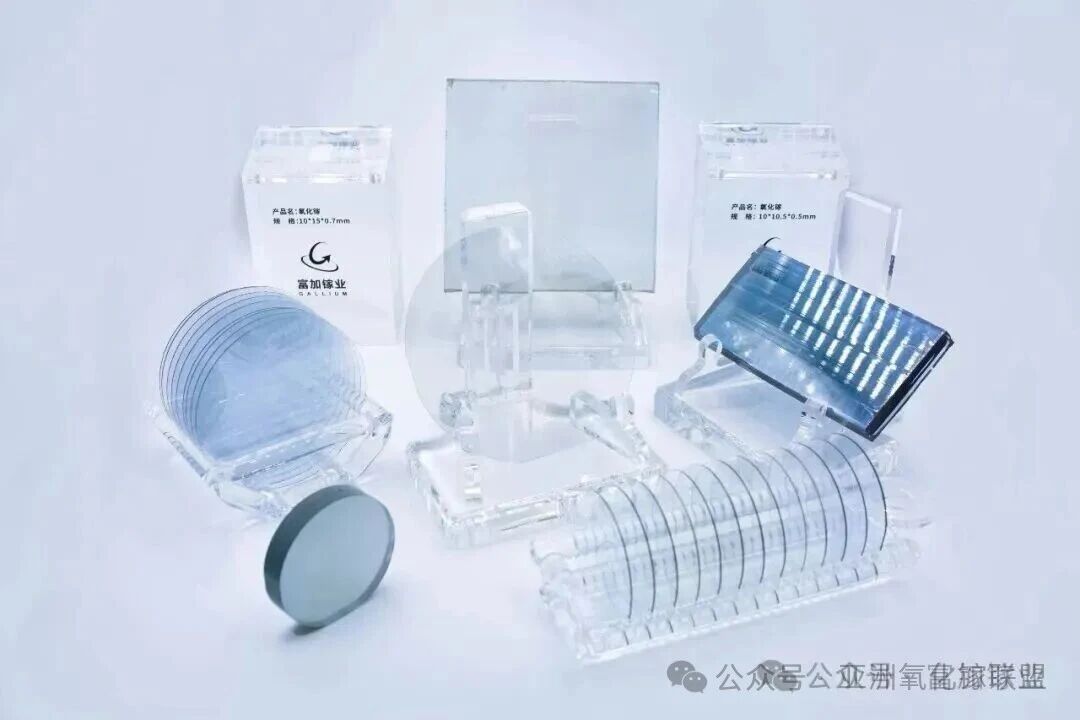
As one of China’s earliest pioneers in gallium oxide single-crystal growth research and a leading supplier in the industry, we are committed to providing global customers with excellent gallium oxide single-crystal substrates. Our product line covers 26 standard gallium oxide substrate products ranging from 2 to 6 inches, and we can provide customized solutions for size, electrical properties, and crystal orientation, meeting the needs of high-quality epitaxial wafer R&D and volume production.
Gallium Oxide Single-Crystal Epitaxy
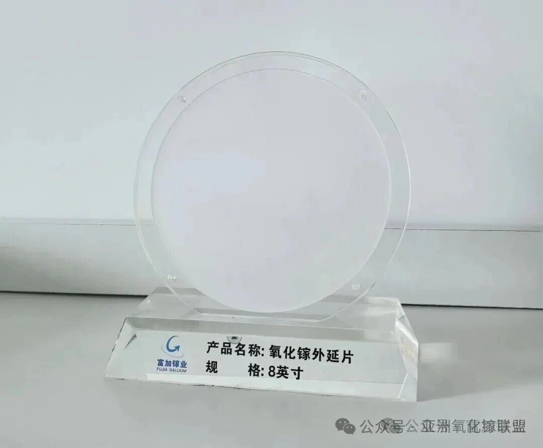
Based on mature MOCVD (metal-organic chemical vapor deposition) and MBE (molecular beam epitaxy) technology platforms, our product line covers 15 standard gallium oxide epitaxial wafer products, including 2-6 inch products, as well as customized MBE gallium oxide epitaxial wafers, providing customers with integrated “substrate-to-epitaxy” solutions. The epitaxial layer growth process adopts a precise process control system and can customize key parameters such as epitaxial layer thickness, doping concentration, and compositional uniformity according to customer needs, meeting the R&D and production requirements of devices with different power ratings and functional types.
Gallium Oxide Single-Crystal Equipment

The company has developed the world’s first EFG (edge-defined film-fed growth) system with a “one-click crystal growth” function, capable of meeting 2-6 inch crystal growth requirements. It currently holds 8 authorized domestic patents and 4 international patents, and can provide equipment and supporting process packages. The company has also independently developed fully automatic VB (vertical Bridgman) crystal growth equipment and was the first in China to overcome the technical bottleneck of 12-inch single-crystal growth, achieving large-size VB single-crystal fabrication. It currently holds 8 authorized domestic patents and 4 international patents, and can provide VB equipment and process packages according to customer needs.
Welcome to Inquire
Fujia Gallium has long been committed to the industrialization of ultra-wide-bandgap semiconductor gallium oxide materials, continuously advancing gallium oxide single-crystal substrates, MOCVD homoepitaxy, and related technologies.
Specific crystal orientation, size, grade, inventory, and gift rules for promotional products are subject to confirmation by sales representatives. Please scan the QR code or call 13506753213 for inquiries, so that every exploration in the new semester is accompanied by high-quality materials. Fujia Gallium will continue to serve scientific research and innovation with reliable products, enabling the world to use superior materials.
About Fujia Gallium
Hangzhou Fujia Gallium Technology Co., Ltd. was established on December 31, 2019. The company takes “Bringing Better Materials to the World” as its vision, and commits to the industrialization of ultra-wide bandgap semiconductor gallium oxide materials.
The company is a national high-tech enterprise, a Zhejiang Provincial specialized, refined, unique and innovative small and medium-sized enterprise, and a "quasi-unicorn" enterprise. It has undertaken many national and provincial-level projects from the Ministry of Science and Technology, National Development and Reform Commission, Ministry of Industry and Information Technology and other departments. It has obtained 67 authorized patents at home and abroad. It is the initiator and the first drafting unit of national standards in China’s gallium oxide industry. A series of important achievements achieved by the company in promoting gallium oxide industrialization have been reported and publicized by well-known media such as CCTV, People’s Daily, Xinhuanet, Science and Technology Daily, China Securities Journal and The Paper.
Instruction
Official Account

Cooperation
Top
