


Recently, Prof. Kui Ma’s team from the Department of Electronic Science and the Engineering Research Center of the Ministry of Education for the Reliability of Semiconductor Power Devices at Guizhou University published their latest work in Applied Surface Science. The paper, entitled “Laser annealing modulates near-surface Cu-related chemical states and band-edge evolution in high-temperature-treated Cu-doped β-Ga2O3 thin films”, investigates the laser-annealing-induced evolution of near-surface Cu-related chemical states and band edges in high-temperature-treated Cu-doped β-Ga2O3 thin films. Yulin Ma, a Ph.D. candidate at Guizhou University, is the first author, and Prof. Kui Ma is the corresponding author. Associate Prof. Fashun Yang of Guizhou University and Lai Yang of Chongqing Semi-chip Electronics Co., Ltd. also contributed to this work.
Background
β-Ga2O3 is a promising material for high-voltage and high-power electronics because of its ultrawide bandgap, high theoretical breakdown field, and availability of large-area single-crystal substrates. However, unlike its well-established n-type conduction, effective acceptor doping and hole transport remain major challenges. The highly localized O 2p-derived valence band favors hole self-trapping, while deep acceptor levels and donor compensation further hinder hole conduction.
Cu offers multiple oxidation states and strong sensitivity to local coordination, making it a potential route for tuning the defect and electronic structures of β-Ga2O3. However, Cu incorporation may also introduce mixed valence states, defect complexes, local segregation, and Cu-rich secondary phases. The relationships among local Cu chemistry, relative band-edge positions, donor–acceptor compensation, and carrier transport therefore remain to be clarified.
To address these issues, the team developed a post-growth strategy combining high-temperature treatment (HTT) with continuous-wave laser annealing (LA). HTT promotes crystallographic ordering, structural relaxation, and elemental redistribution, while subsequent 1080 nm continuous-wave LA further tunes the local structural and chemical environments. By integrating structural characterization, XPS, optical spectroscopy, Hall measurements, and device testing, the study systematically evaluates how Cu input affects crystal structure, band-edge evolution, carrier compensation, and device response.
Abstract
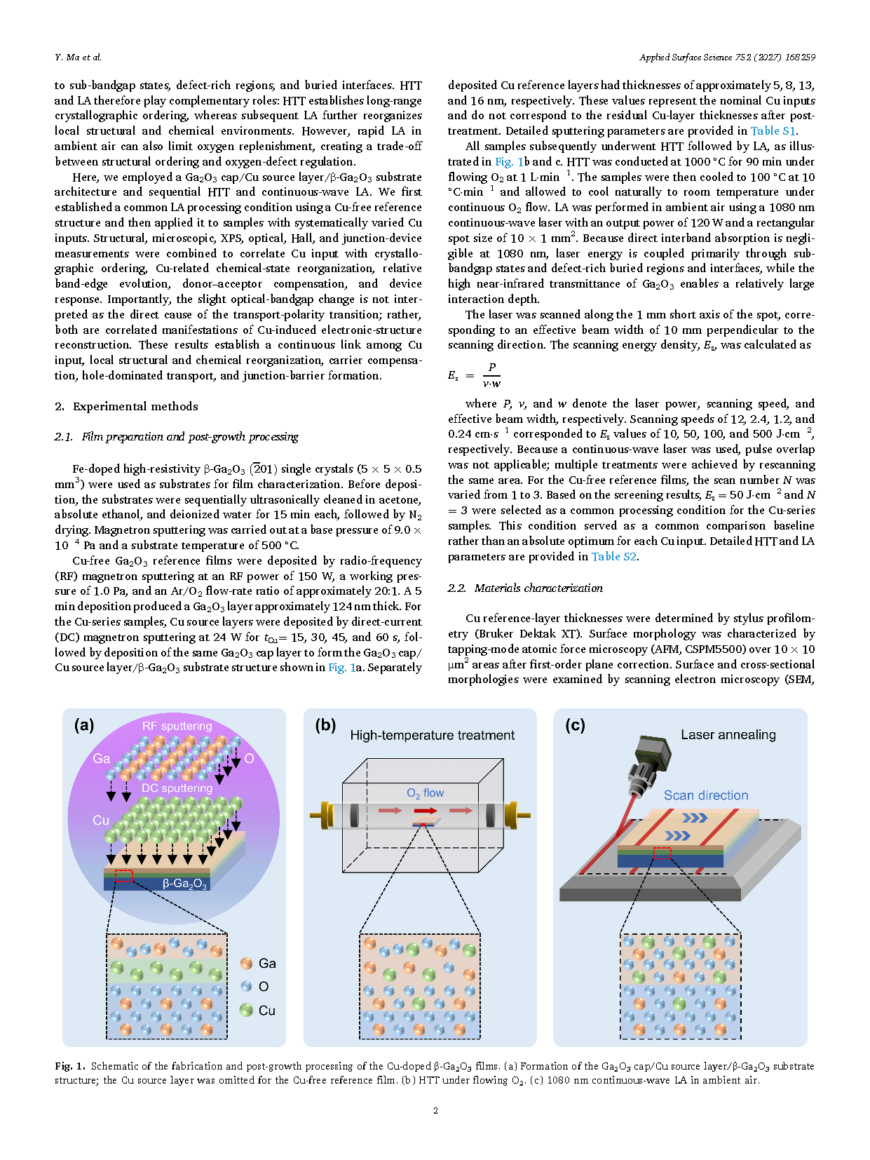
Building on the team’s granted invention patent, “A Method for Incorporating Metal Atoms into Gallium Oxide Materials” (ZL202111453562.8), the study employed a Ga2O3 cap/Cu source layer/β-Ga2O3 substrate architecture and introduced a combined post-growth strategy of high-temperature treatment (HTT) and 1080 nm continuous-wave laser annealing (LA). The work systematically examined how Cu input influences film structure, local chemical states, relative band-edge positions, electrical transport, and device performance.
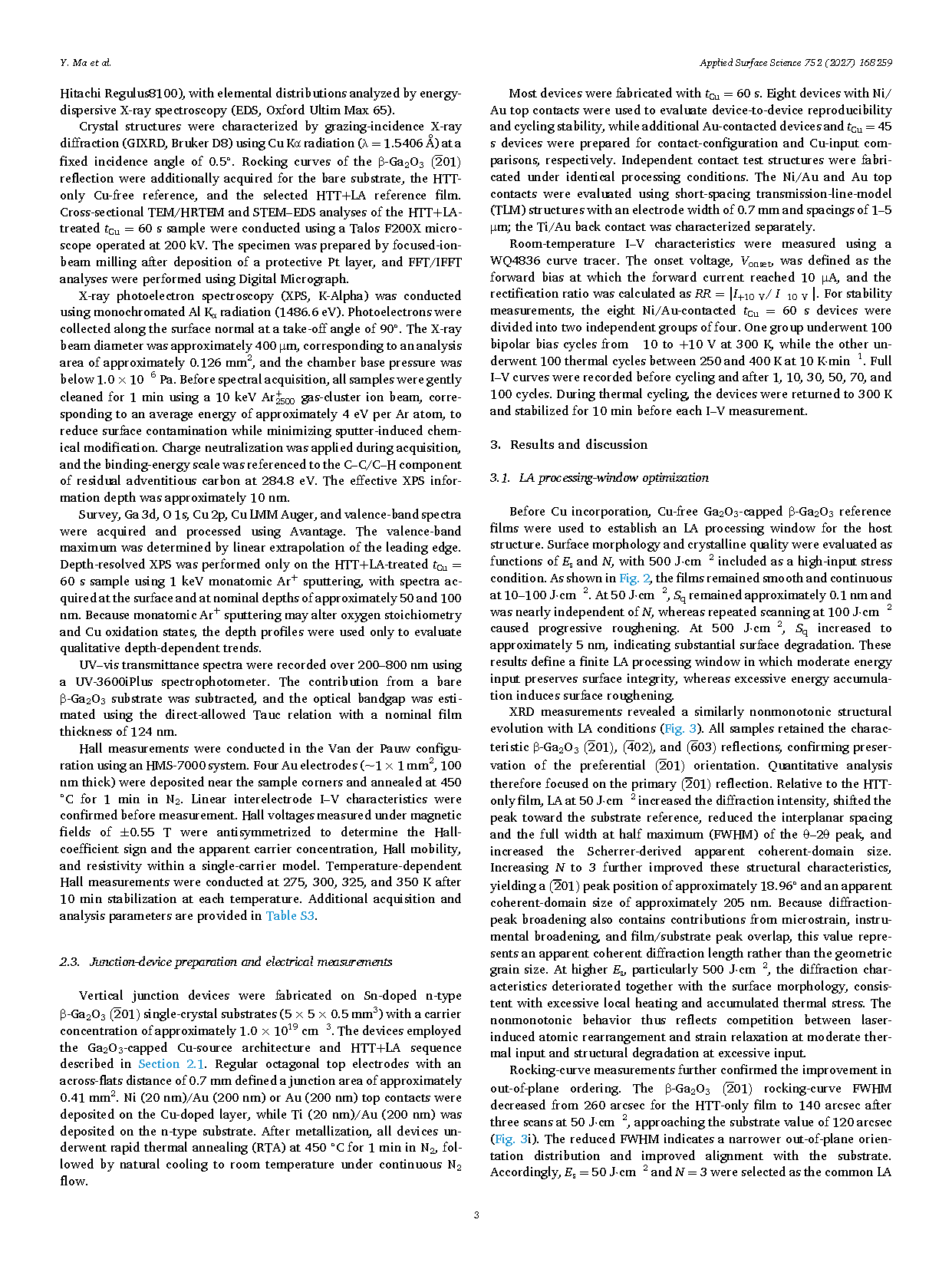
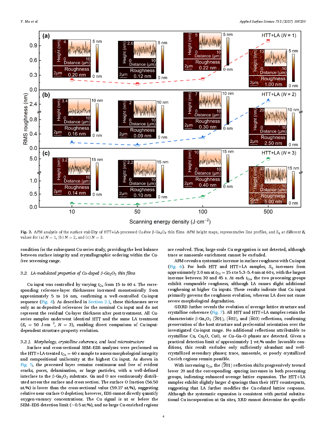
The LA conditions were first optimized using Cu-free reference samples. A scanning energy density of 50 J·cm−2 with three scans was selected as the common LA condition, reducing the β-Ga2O3 (−201) rocking-curve FWHM from 260 to 140 arcsec while preserving surface integrity, indicating markedly improved crystallographic ordering. With increasing Cu input, the β-Ga2O3 host lattice was maintained, accompanied by mild anisotropic lattice expansion. LA further enhanced crystalline coherence and reorganized the near-surface Cu environment toward predominantly CuO-like, Cu2+-dominated coordination.
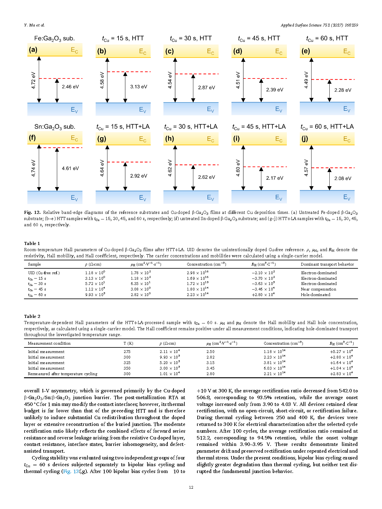
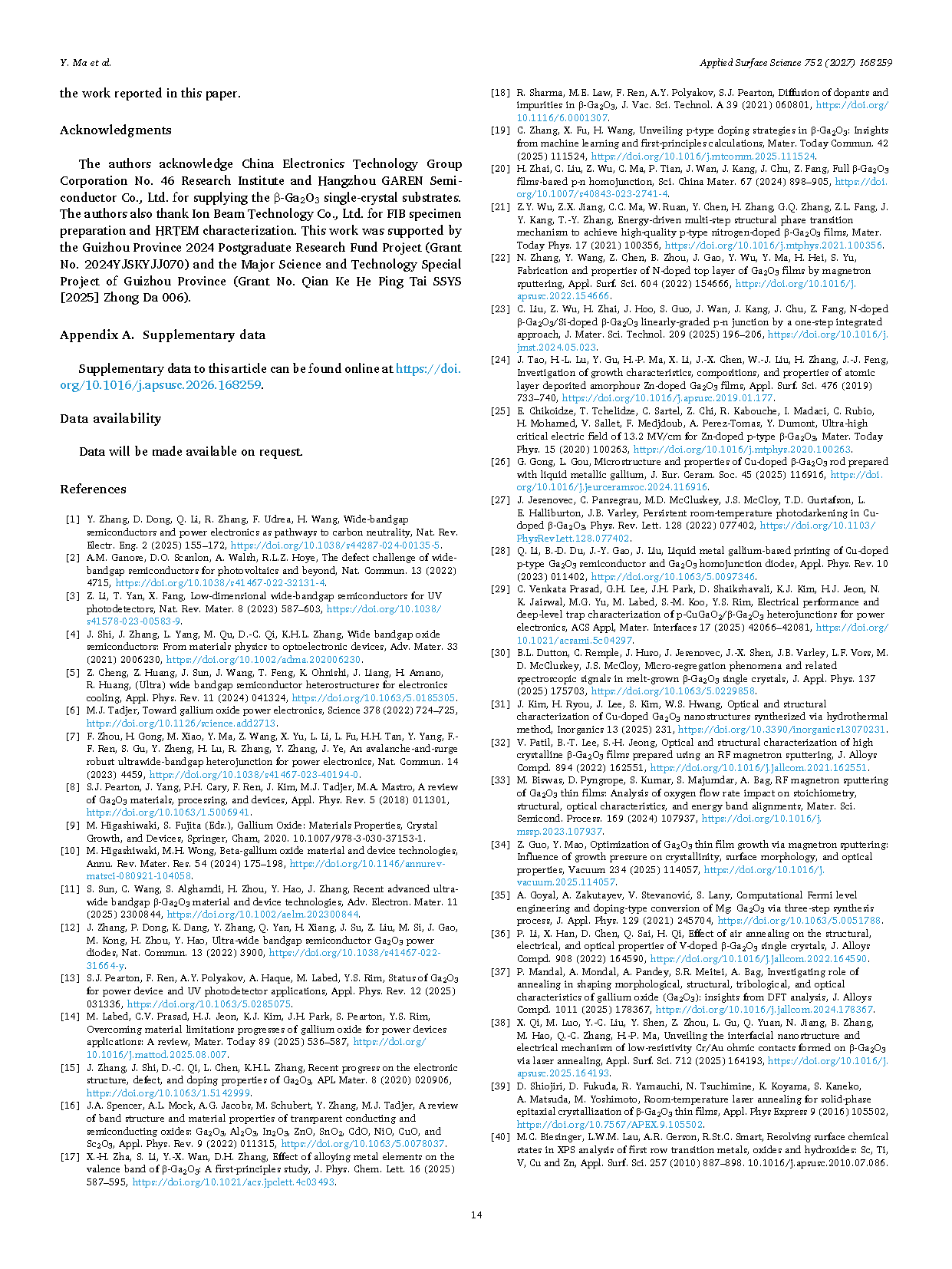
Optical and valence-band XPS measurements showed only minor changes in the optical bandgap, but a pronounced reduction in the relative energy separation between the Fermi level and the valence-band maximum, indicating progressively stronger donor–acceptor compensation. Hall measurements further revealed a transport transition from electron-dominated to near-compensated and ultimately hole-dominated behavior with increasing Cu input. The tCu = 60 s sample maintained a positive Hall coefficient over 275–350 K. Consistent with this transport evolution, the junction response changed from nearly linear I–V behavior at tCu = 45 s to pronounced rectification at 60 s. Across eight devices, the average onset voltage was approximately 3.9 V and the average rectification ratio reached 542, with 93.5% and 94.5% of the initial rectification retained after 100 bipolar-bias and thermal cycles, respectively.
Highlights
Established a synergistic HTT–continuous-wave LA strategy.A unified LA processing window was first defined using Cu-free reference samples. The optimized treatment significantly improved the crystallographic ordering of β-Ga2O3 while preserving surface integrity, providing a stable and consistent basis for subsequent Cu-doped film studies.
Revealed the LA-induced reorganization of the local Cu chemical environment. Combined Cu 2p and Cu LMM Auger analyses showed that LA drives the near-surface Cu environment toward predominantly CuO-like, Cu2+-dominated coordination while retaining the β-Ga2O3host lattice. This demonstrates that LA not only improves crystal quality but also actively tunes local chemical states.
Established a “structure–chemical state–band edge–transport–device” correlation involving LA. Under a common LA condition, increasing Cu input markedly reduced the relative Fermi-level-to-valence-band-maximum separation and strengthened donor–acceptor compensation, driving transport from electron-dominated through near compensation to hole-dominated behavior. This evolution was further reflected in pronounced and stable junction rectification, linking material-level modulation to device-level performance.
Conclusion
The study developed a post-growth strategy that combines high-temperature treatment with laser annealing to regulate Cu-doped β-Ga2O3 thin films. The results show that optimized LA conditions can further improve crystallographic ordering while preserving surface integrity, and simultaneously promote the reorganization of Cu-related local structures, chemical environments, and defect states. With increasing Cu input, the relative band-edge position and donor–acceptor compensation evolve continuously, driving carrier transport from electron-dominated through near compensation to hole-dominated behavior. The resulting films also exhibit stable junction rectification on n-type β-Ga2O3 substrates. Overall, this work establishes a continuous link among Cu input, local structural and chemical-state reorganization, band-edge evolution, carrier compensation, hole-dominated transport, and device response, providing new experimental insights and a practical route for further tuning Cu-doped β-Ga2O3 materials and related junction devices through laser annealing.
Project Support
This work was supported by the Major Science and Technology Special Project of Guizhou Province (Grant No. Qian Ke He Ping Tai SSYS [2025] Zhong Da 006) and the Guizhou Province 2024 Postgraduate Research Fund Project (Grant No. 2024YJSKYJJ070). The authors also gratefully acknowledge China Electronics Technology Group Corporation No. 46 Research Institute and Hangzhou GAREN Semiconductor Co., Ltd. for providing the β-Ga2O3 single-crystal substrates.
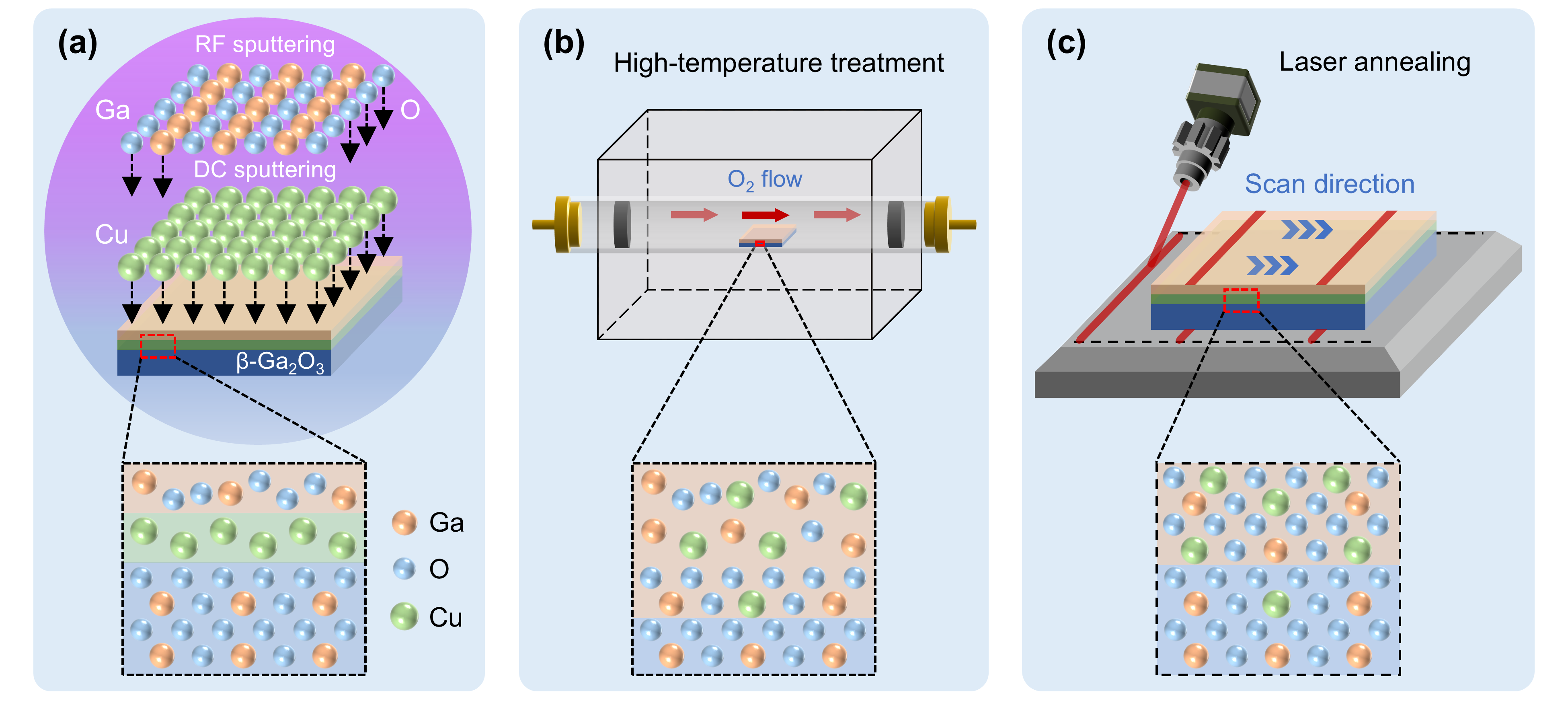
Fig. 1. Schematic of the fabrication and post-growth processing of the Cu-doped β-Ga2O3 films. (a) Formation of the Ga2O3 cap/Cu source layer/β-Ga2O3 substrate structure; the Cu source layer was omitted for the Cu-free reference film. (b) HTT under flowing O2. (c) 1080 nm continuous-wave LA in ambient air.
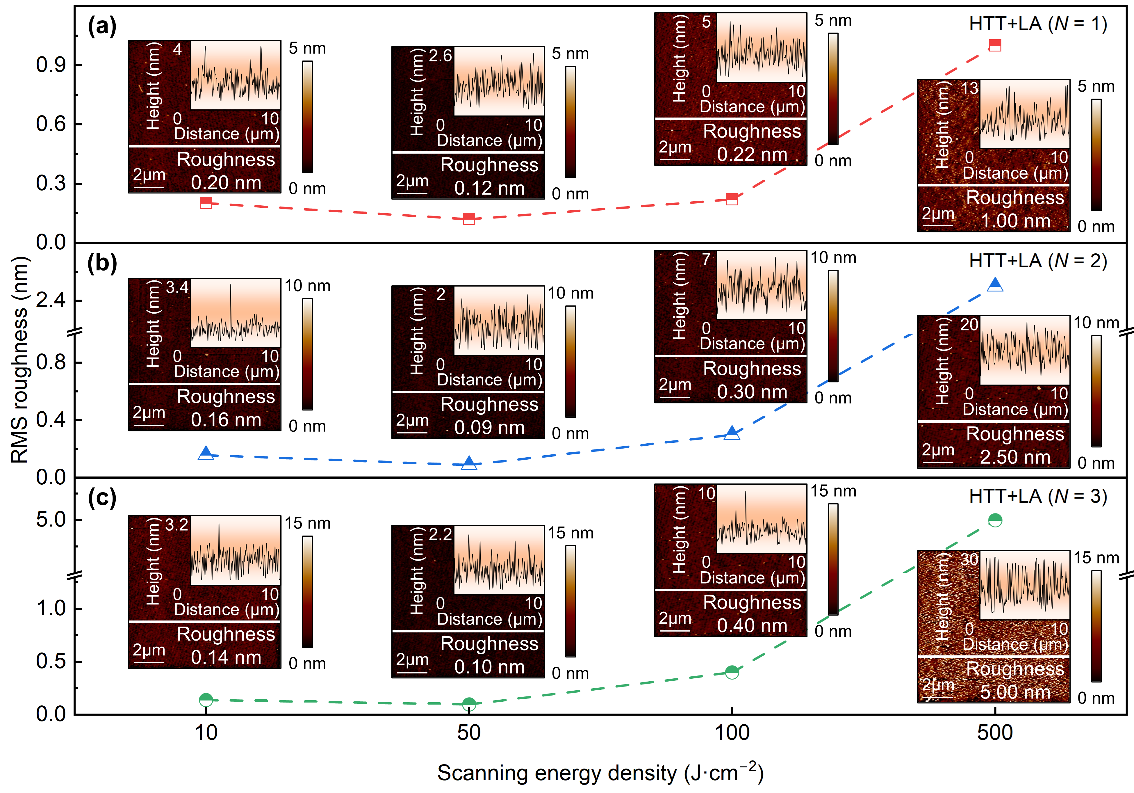
Fig. 2. AFM analysis of the surface stability of HTT+LA-processed Cu-free β-Ga2O3 thin films. AFM height maps, representative line profiles, and Sq at different Es values for (a) N = 1, (b) N = 2, and (c) N = 3.
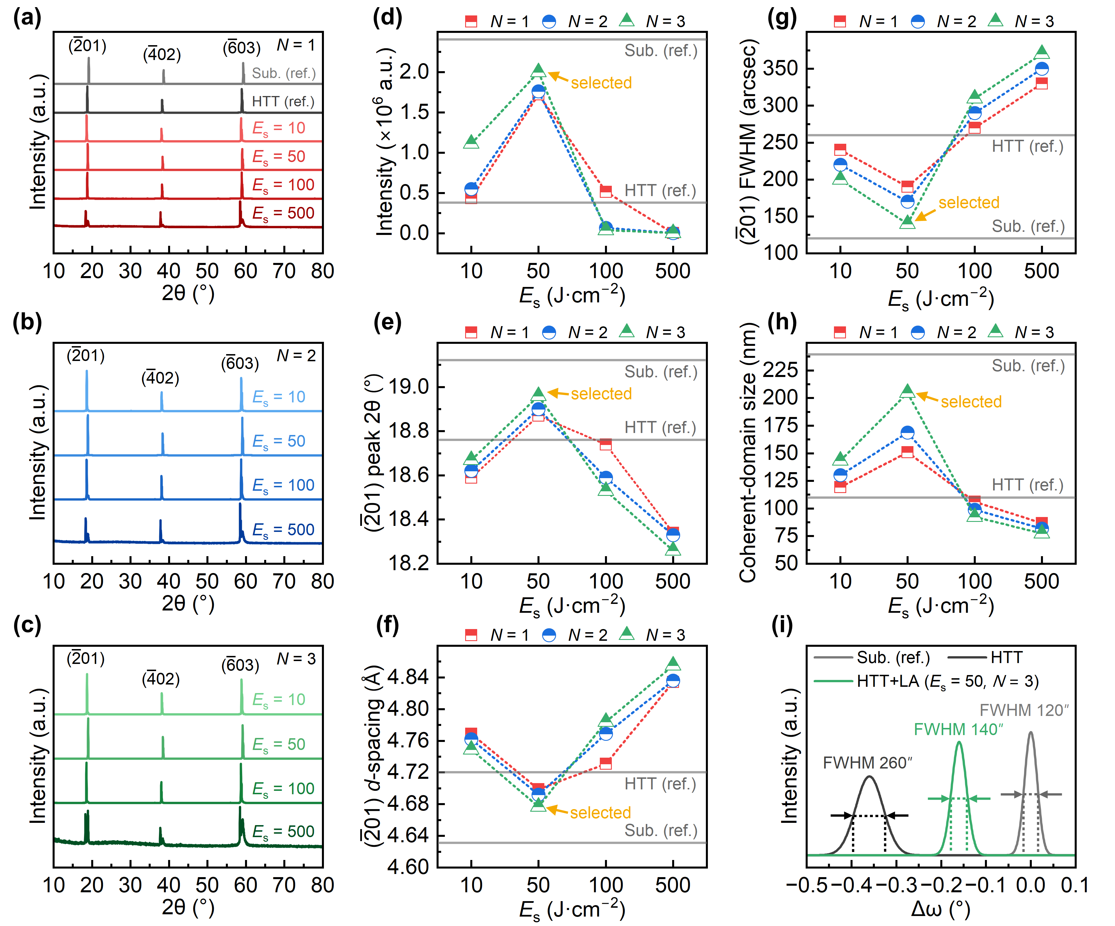
Fig. 3. XRD evaluation of the LA processing window. (a–c) XRD θ–2θ patterns obtained at different Es values for N = 1, 2, and 3, respectively. (d–h) (−201) peak intensity, peak position, interplanar spacing, θ–2θ peak FWHM, and Scherrer-derived apparent coherent-domain size as functions of Es. (i) Representative rocking curves of the substrate reference, HTT-only film, and selected HTT+LA film.

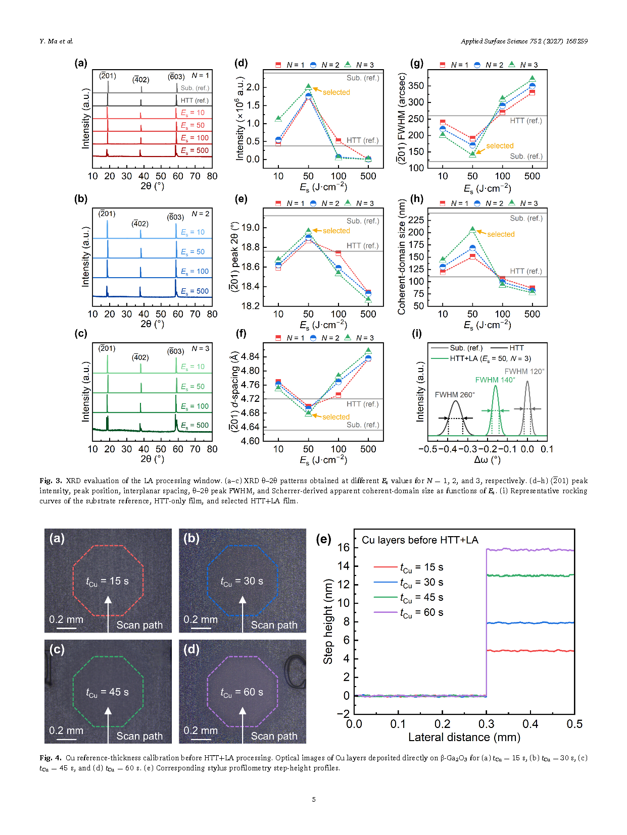
Fig. 4. Cu reference-thickness calibration before HTT+LA processing. Optical images of Cu layers deposited directly on β-Ga2O3 for (a) tCu = 15 s, (b) tCu = 30 s, (c) tCu = 45 s, and (d) tCu = 60 s. (e) Corresponding stylus profilometry step-height profiles.
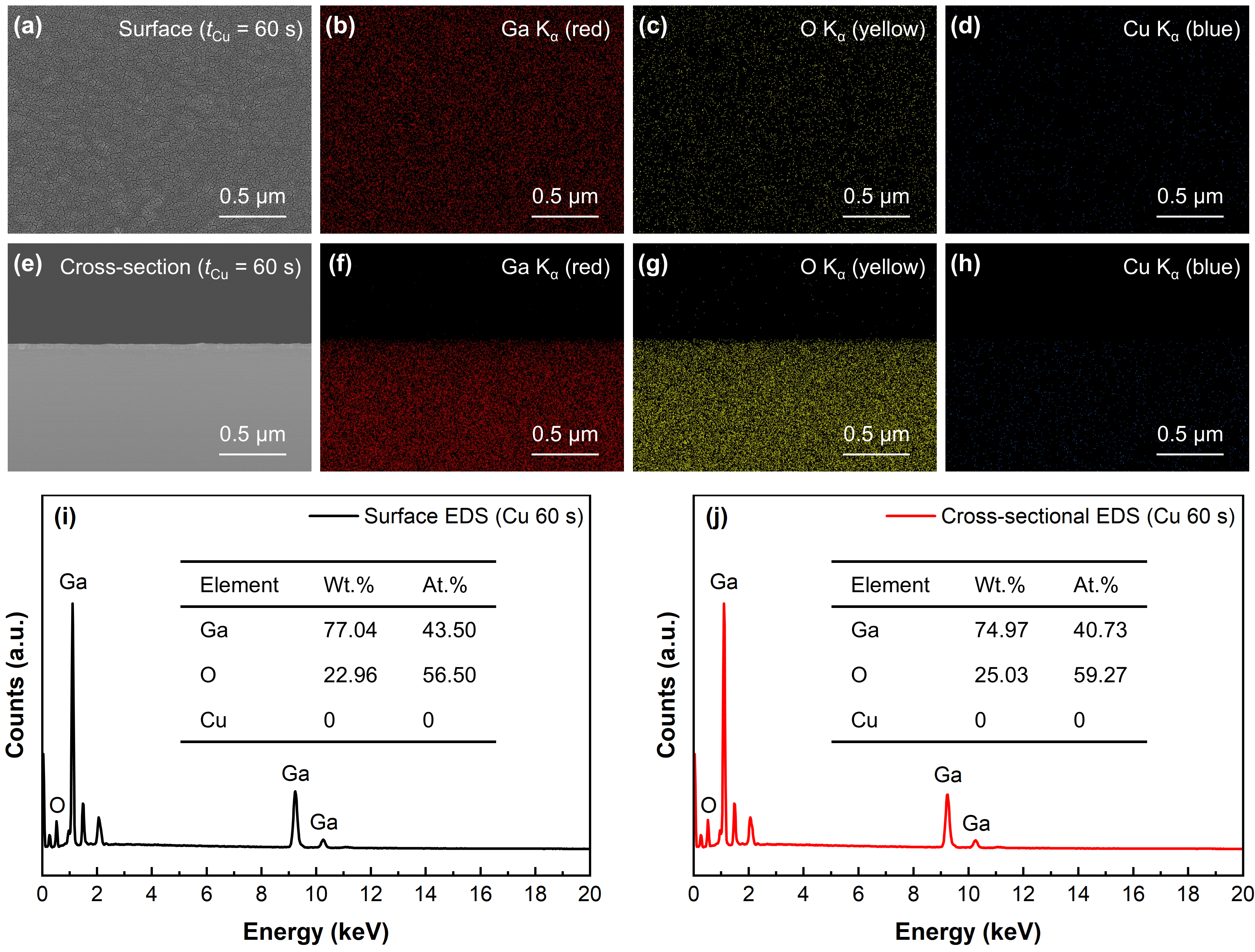
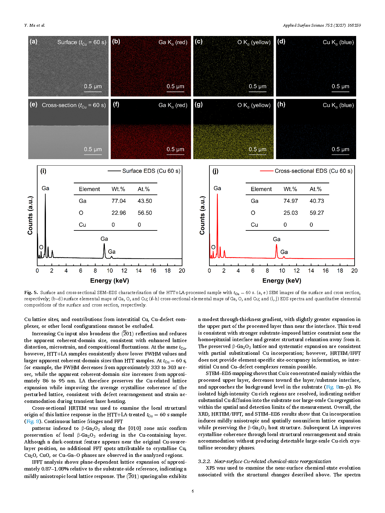
Fig. 5. Surface and cross-sectional SEM–EDS characterization of the HTT+LA-processed sample with tCu = 60 s. (a, e) SEM images of the surface and cross section, respectively; (b–d) surface elemental maps of Ga, O, and Cu; (f–h) cross-sectional elemental maps of Ga, O, and Cu; and (i, j) EDS spectra and quantitative elemental compositions of the surface and cross section, respectively.

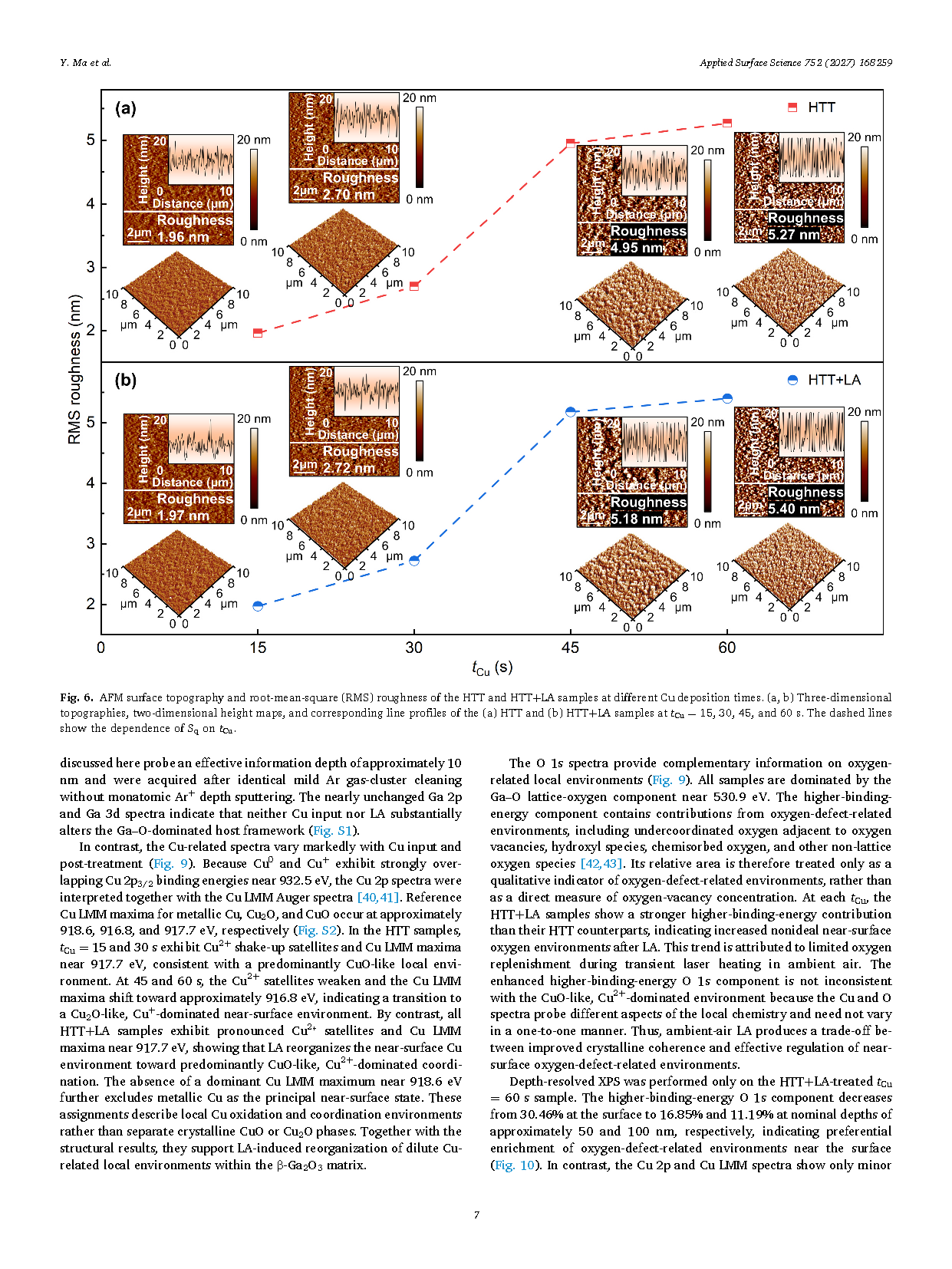
Fig. 6. AFM surface topography and root-mean-square (RMS) roughness of the HTT and HTT+LA samples at different Cu deposition times. (a, b) Three-dimensional topographies, two-dimensional height maps, and corresponding line profiles of the (a) HTT and (b) HTT+LA samples at tCu = 15, 30, 45, and 60 s. The dashed lines show the dependence of Sq on tCu.
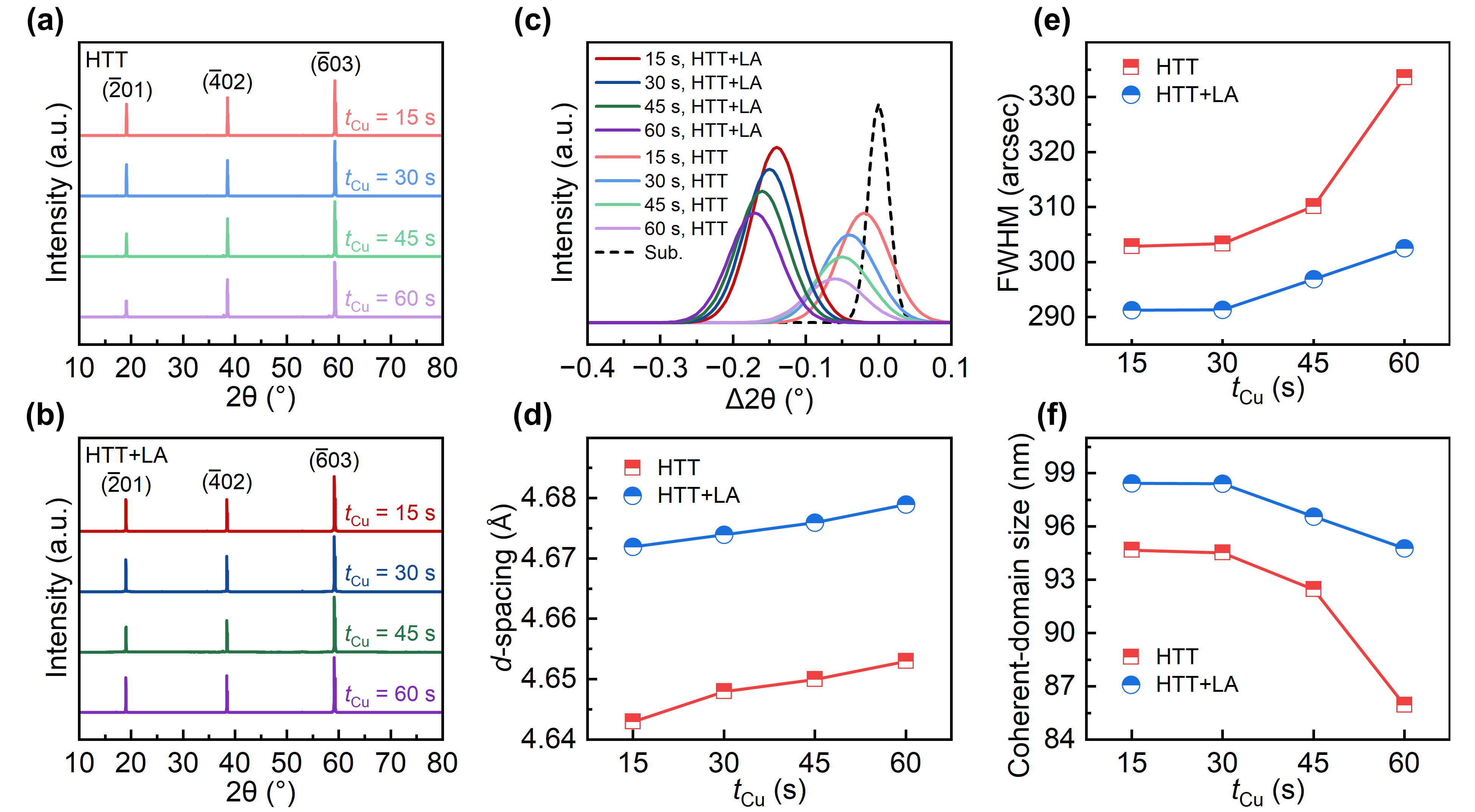
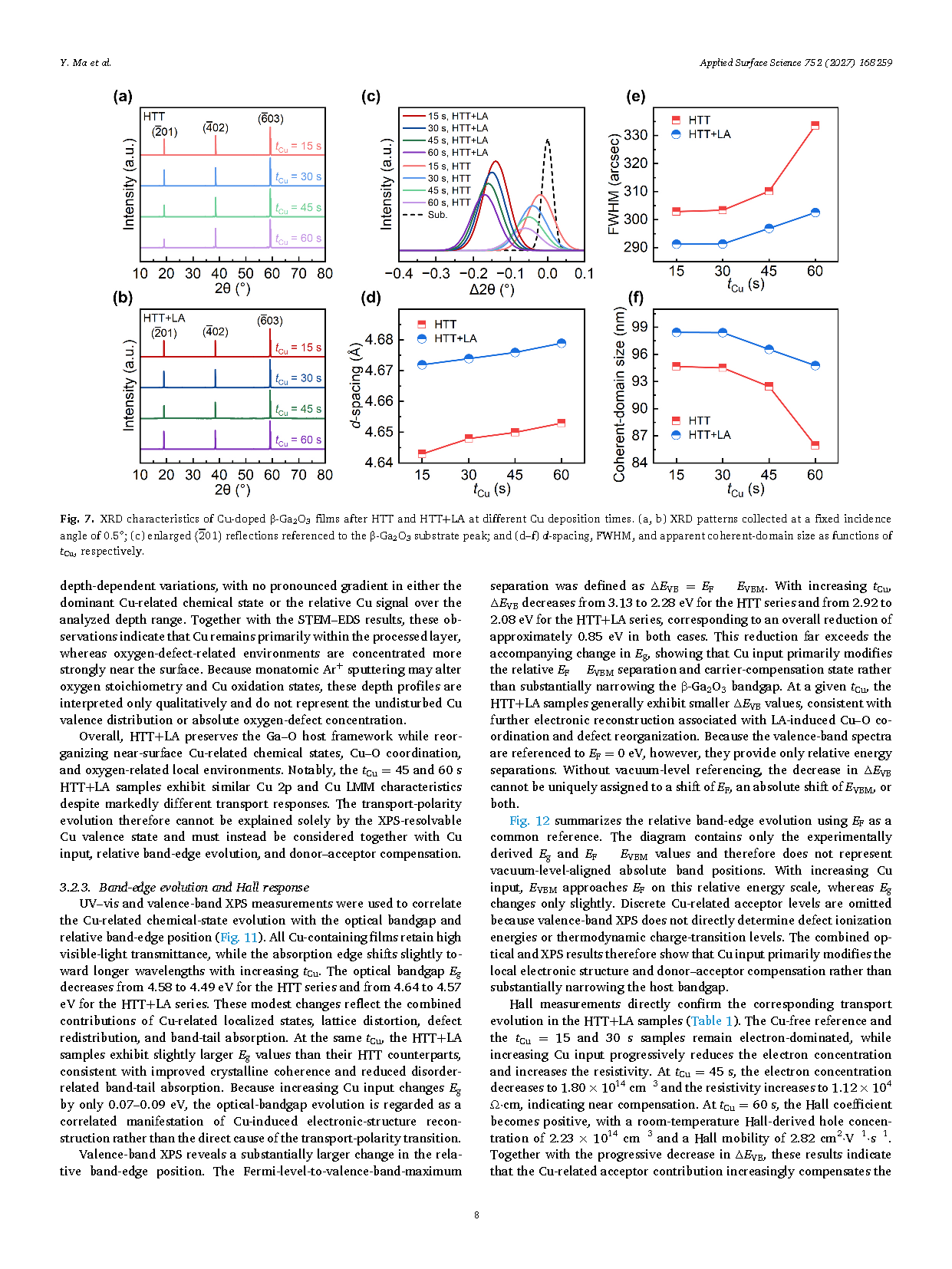
Fig. 7. XRD characteristics of Cu-doped β-Ga2O3 films after HTT and HTT+LA at different Cu deposition times. (a, b) XRD patterns collected at a fixed incidence angle of 0.5°; (c) enlarged (−201) reflections referenced to the β-Ga2O3 substrate peak; and (d–f) d-spacing, FWHM, and apparent coherent-domain size as functions of tCu, respectively.

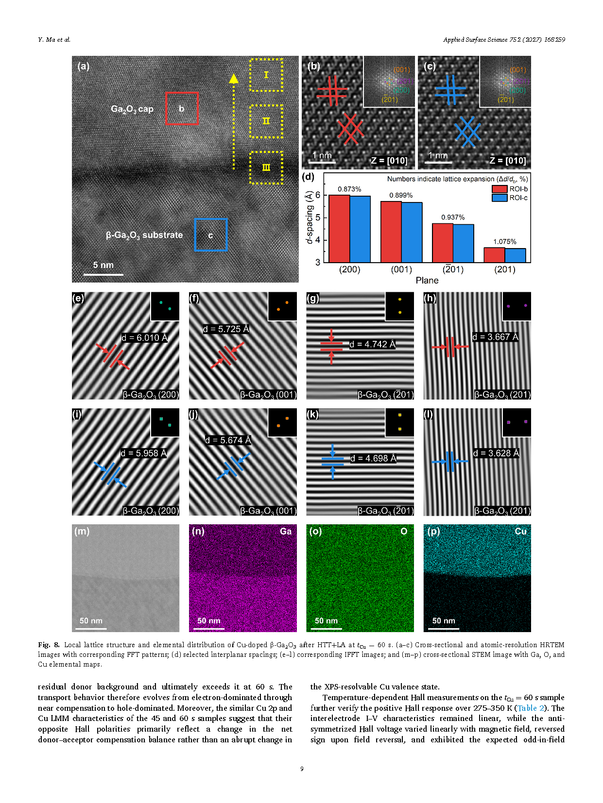
Fig. 8. Local lattice structure and elemental distribution of Cu-doped β-Ga2O3 after HTT+LA at tCu = 60 s. (a–c) Cross-sectional and atomic-resolution HRTEM images with corresponding FFT patterns; (d) selected interplanar spacings; (e–l) corresponding IFFT images; and (m–p) cross-sectional STEM image with Ga, O, and Cu elemental maps.
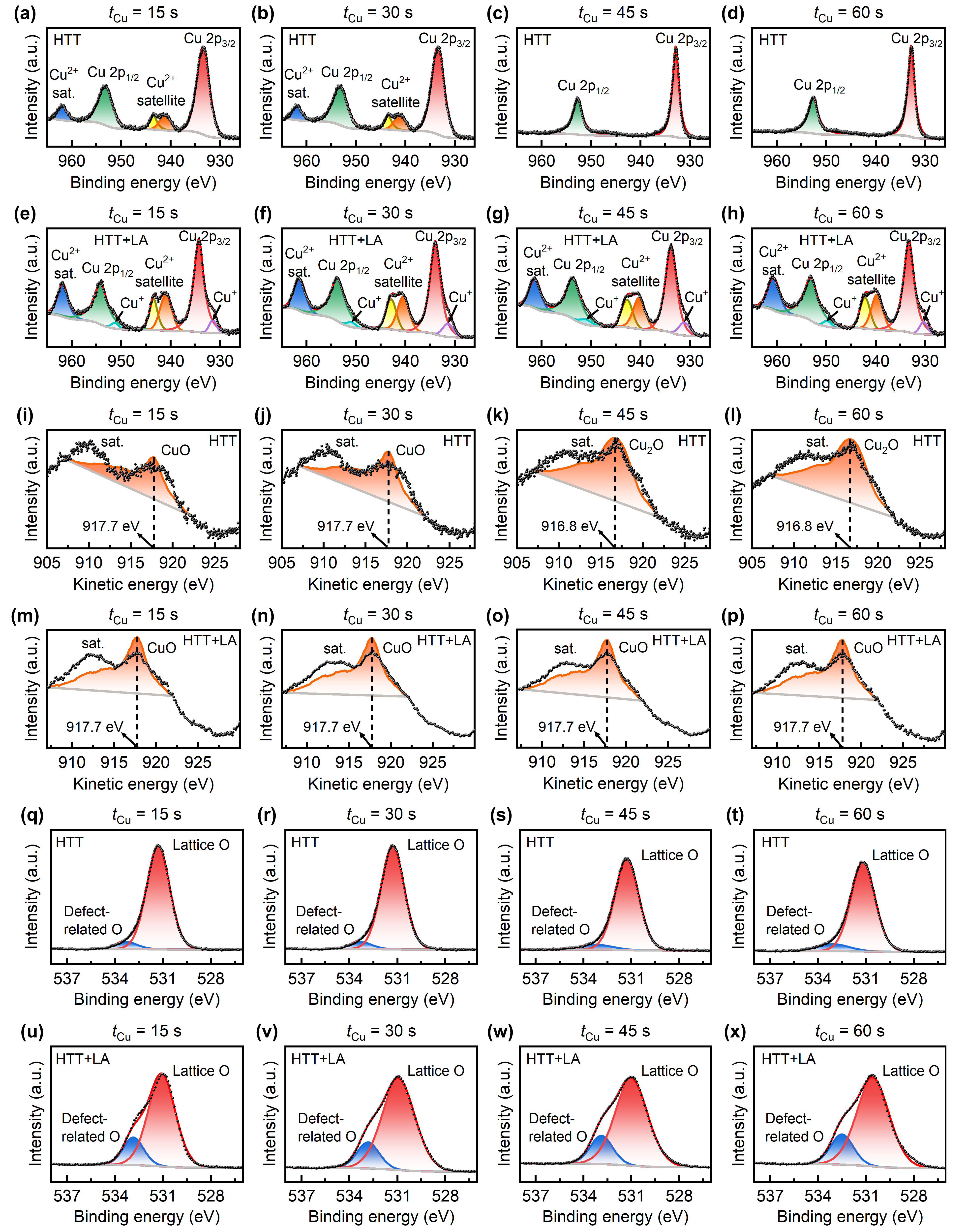
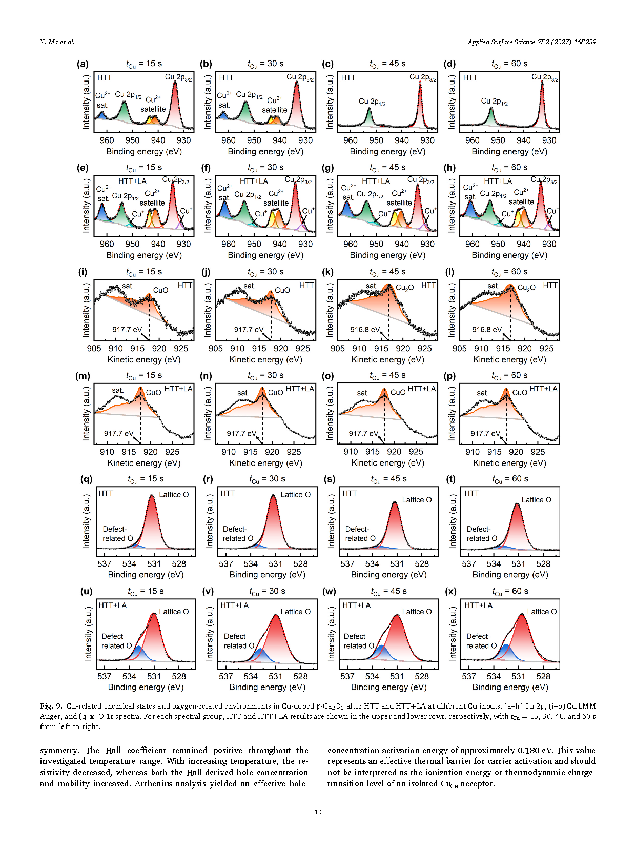
Fig. 9. Cu-related chemical states and oxygen-related environments in Cu-doped β-Ga2O3 after HTT and HTT+LA at different Cu inputs. (a–h) Cu 2p, (i–p) Cu LMM Auger, and (q–x) O 1s spectra. For each spectral group, HTT and HTT+LA results are shown in the upper and lower rows, respectively, with tCu = 15, 30, 45, and 60 s from left to right.
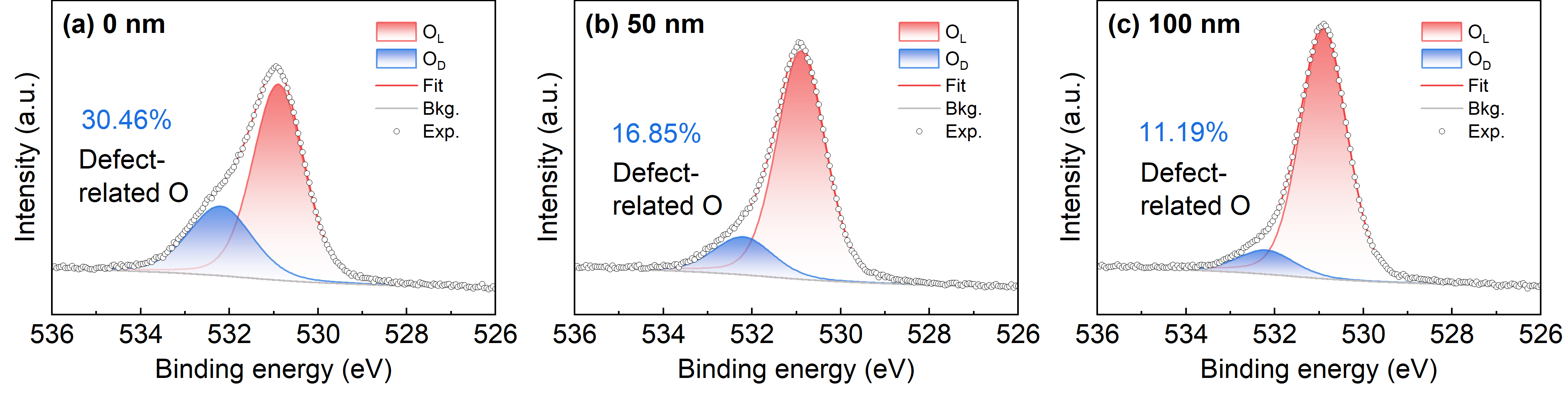
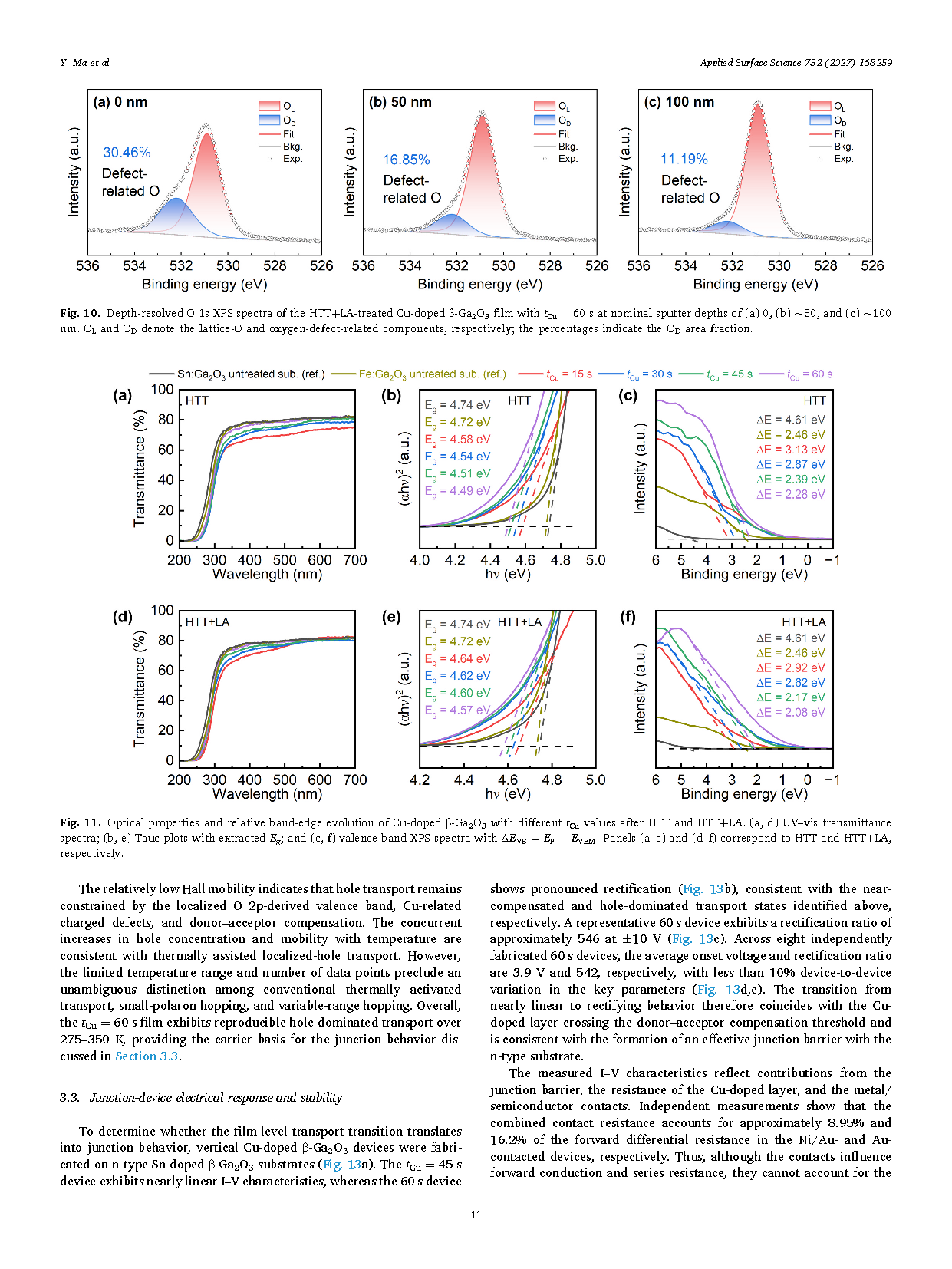
Fig. 10. Depth-resolved O 1s XPS spectra of the HTT+LA-treated Cu-doped β-Ga2O3 film with tCu = 60 s at nominal sputter depths of (a) 0, (b) ~50, and (c) ~100 nm. OL and OD denote the lattice-O and oxygen-defect-related components, respectively; the percentages indicate the OD area fraction.
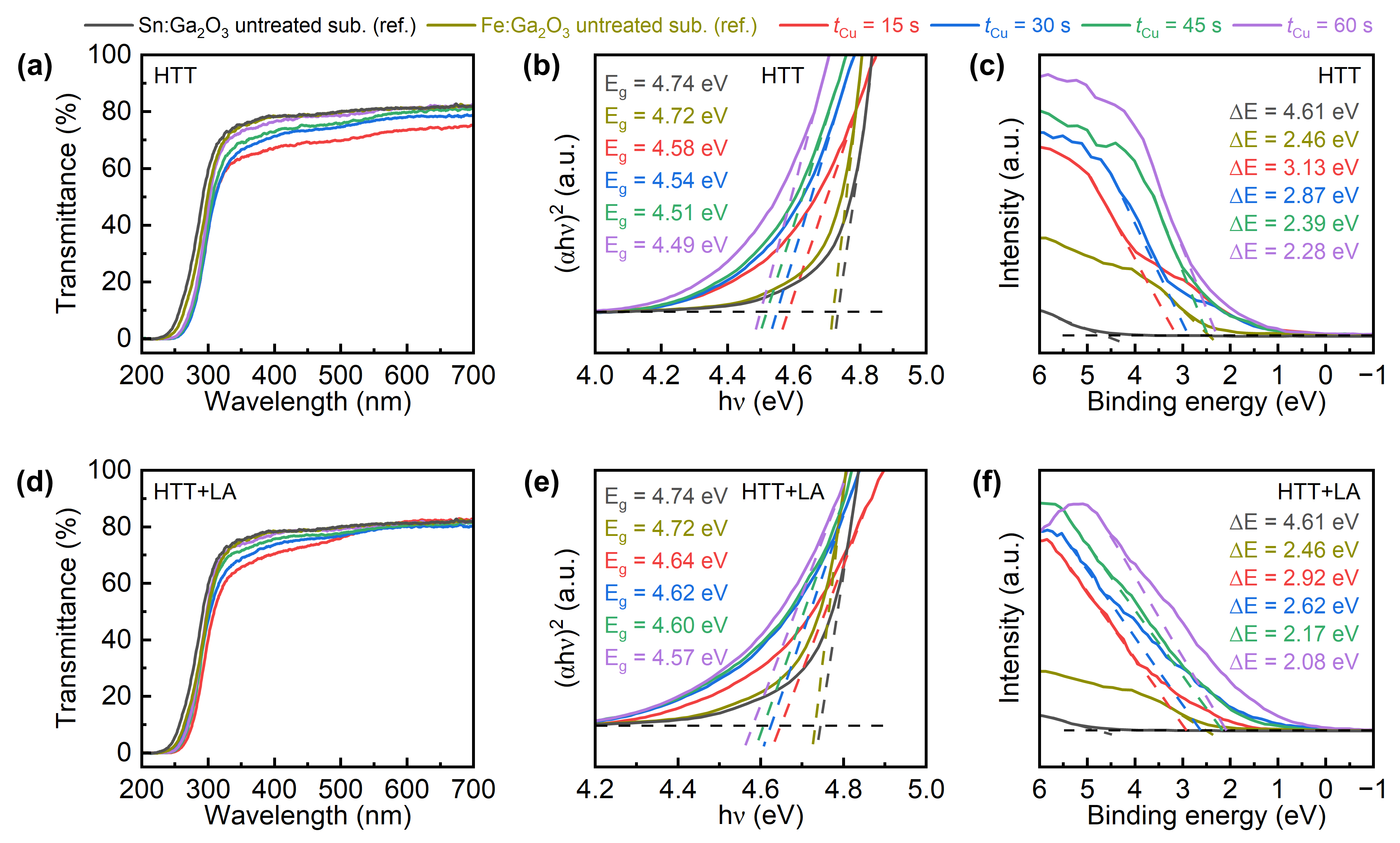
Fig. 11. Optical properties and relative band-edge evolution of Cu-doped β-Ga2O3 with different tCu values after HTT and HTT+LA. (a, d) UV–vis transmittance spectra; (b, e) Tauc plots with extracted Eg; and (c, f) valence-band XPS spectra with ΔEVB = EF − EVBM. Panels (a–c) and (d–f) correspond to HTT and HTT+LA, respectively.
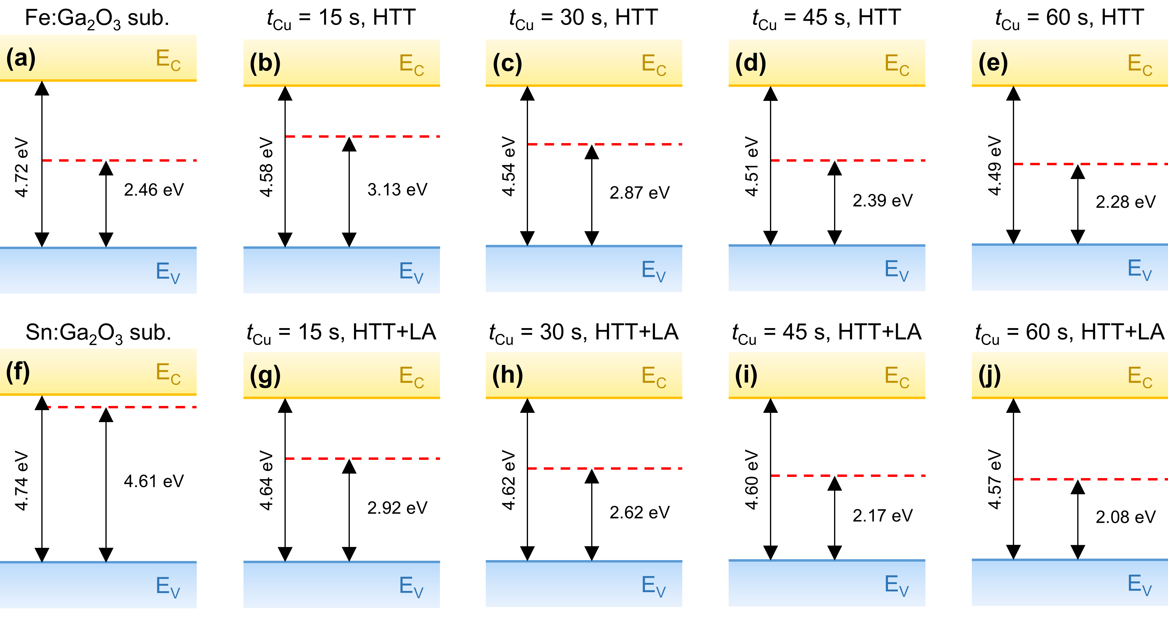
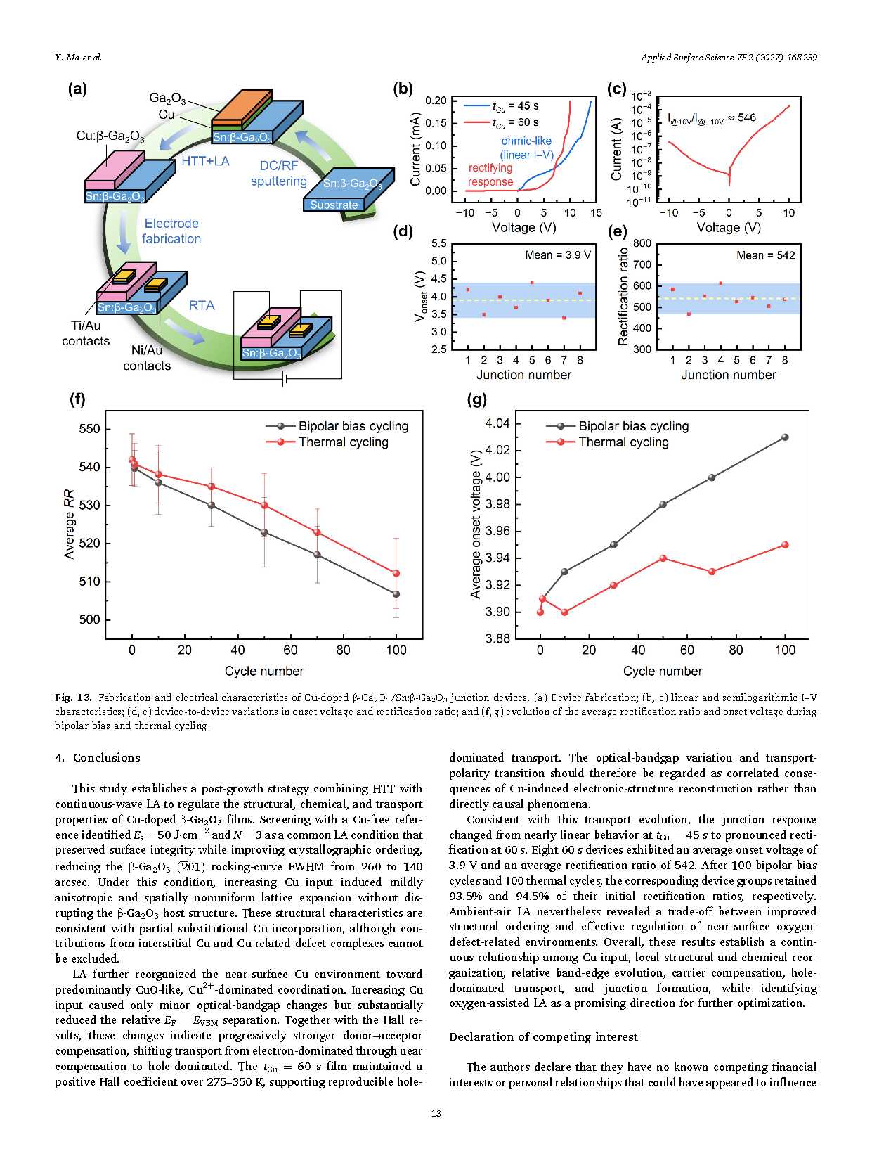
Fig. 12. Relative band-edge diagrams of the reference substrates and Cu-doped β-Ga2O3 films at different Cu deposition times. (a) Untreated Fe-doped β-Ga2O3 substrate; (b–e) HTT samples with tCu = 15, 30, 45, and 60 s, respectively; (f) untreated Sn-doped β-Ga2O3 substrate; and (g–j) HTT+LA samples with tCu = 15, 30, 45, and 60 s, respectively.
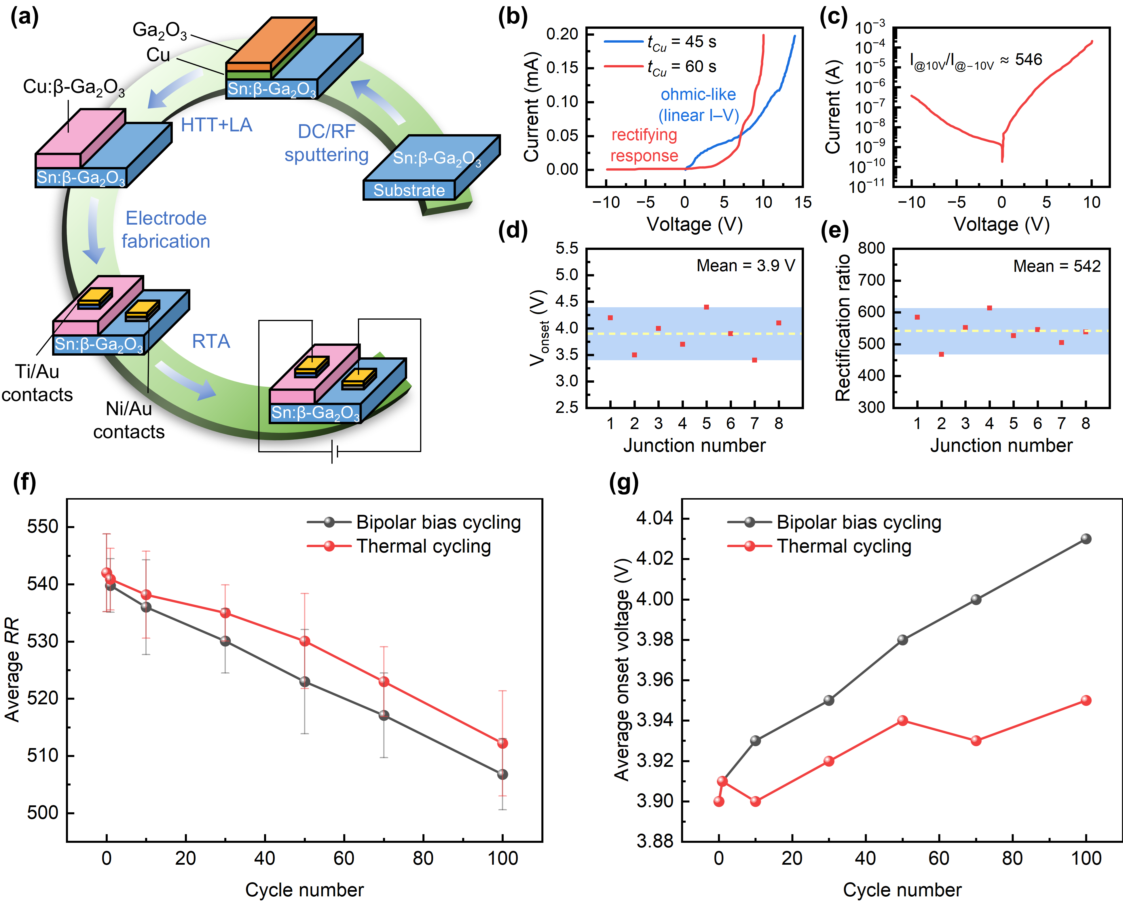
Fig. 13. Fabrication and electrical characteristics of Cu-doped β-Ga2O3/Sn:β-Ga2O3 junction devices. (a) Device fabrication; (b, c) linear and semilogarithmic I–V characteristics; (d, e) device-to-device variations in onset voltage and rectification ratio; and (f, g) evolution of the average rectification ratio and onset voltage during bipolar bias and thermal cycling.
Team Introduction

Corresponding Author: Kui Ma, Professor and Ph.D. Supervisor in the Department of Electronic Science at Guizhou University, and Deputy Director of the Engineering Research Center of the Ministry of Education for the Reliability of Semiconductor Power Devices. His research focuses on power devices and reliability, semiconductor integration technologies, and analog and mixed-signal integrated circuits.
DOI:
doi.org/10.1016/j.apsusc.2026.168259
Instruction
Official Account

Cooperation
Top
