


Recently, Hangzhou Garen Semiconductor Co., Ltd. (hereinafter referred to as “Garen Semiconductor”) achieved the world’s first constant-diameter growth of 12-inch Ga₂O₃ crystals using its independently developed SCIENCE-series VB crystal-growth equipment.
Following the global launch of its 8-inch Ga₂O₃ substrates and homoepitaxial wafers, this achievement marks another significant milestone for the company in the development of large-size Ga₂O₃ materials.
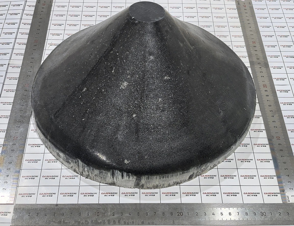
Figure 1. 12-inch Ga₂O₃ crystal developed by Garen Semiconductor
Constant-diameter growth is an important step toward the industrialization of bulk crystals. Only when a crystal ingot develops a section with a uniform diameter can it provide a continuous and stable portion that is suitable for direct slicing, grinding, and polishing. The thicker the constant-diameter section, the more qualified substrate wafers can be sliced from a single ingot, thereby reducing the cost per wafer.
Meanwhile, 12-inch Ga₂O₃ substrates offer a high degree of compatibility with mainstream silicon production lines, potentially reducing downstream equipment investment and production-line transition costs while shortening R&D cycles.
This marks a simultaneous breakthrough by Garen Semiconductor in both crystal diameter and ingot thickness, creating further potential for reducing the cost of Ga₂O₃ substrates.
The VB method is a “crucible-based” crystal-growth technique in which the melt solidifies layer by layer from bottom to top at the solid–liquid interface, enabling the entire melt within the crucible to undergo directional crystallization into a single crystal. The VB method is regarded as one of the promising approaches for large-scale Ga₂O₃ crystal growth and offers several advantages.
The crystal is formed in a single growth process within a closed crucible, resulting in a relatively simple process without complex operations and providing greater flexibility in crystal-orientation selection. The crucible can also effectively suppress defects such as dislocations and twins induced by the anisotropy of Ga₂O₃, contributing to higher growth yield. In addition, the VB method offers a stable thermal field and low operating costs.
However, translating these inherent advantages into the constant-diameter growth of 12-inch crystals is far from straightforward. In practical growth processes, challenges remain in areas such as thermal-field control and process matching.
Garen Semiconductor’s independently developed SCIENCE-series VB crystal-growth equipment achieves temperature-control precision of ±0.1 °C and integrates the equipment with a proprietary process package, enabling the company to address these challenges systematically and rapidly iterate its crystal-growth capabilities from 2-inch to 12-inch crystals.
The equipment has now been delivered to multiple key customers and has received broad recognition from customers and the market for its stable and reliable performance. It has also received the “Outstanding Market Performance Award” from CSPSD.
In March this year, the company achieved the world’s first 8-inch Ga₂O₃ homoepitaxial growth, with the results receiving authoritative certification from third-party institutions in China and abroad. The breakthrough in constant-diameter growth of 12-inch Ga₂O₃ crystals further strengthens the company’s technological advantages in large-size Ga₂O₃ materials.
Going forward, Garen Semiconductor will continue to advance the processing and performance validation of 12-inch Ga₂O₃ ingots, accelerating the transition of Ga₂O₃ substrates from laboratory-scale development toward high-volume production.
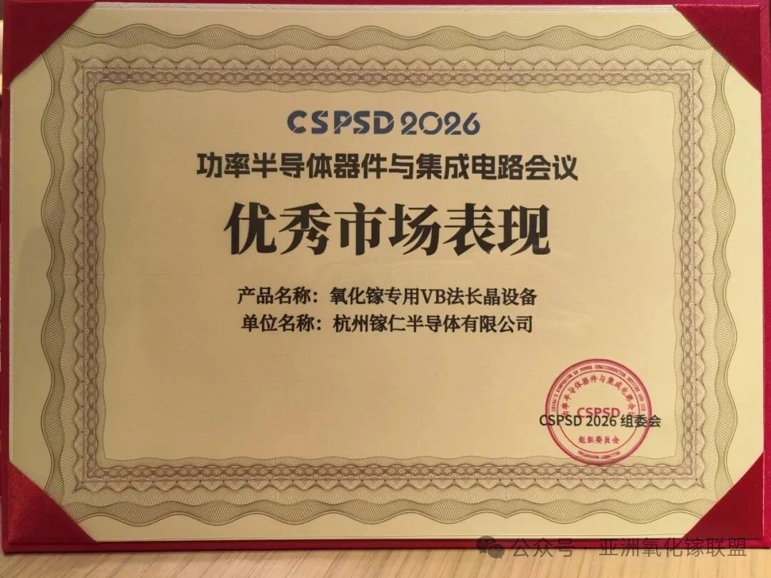
Figure 2. “Outstanding Market Performance” award plaque for Garen Semiconductor’s dedicated Ga₂O₃ VB crystal-growth equipment
About Garen Semiconductor
Hangzhou Garen Semiconductor Co., Ltd. is a global provider of gallium oxide materials and equipment solutions, specializing in the R&D and commercialization of ultra-wide-bandgap semiconductor technologies. The company’s core products include 2‑ to 12‑inch gallium oxide single crystals and substrates (featuring the world’s first constant‑diameter‑growth for both 8‑inch and 12‑inch sizes), vertical Bridgman (VB) gallium oxide crystal growth equipment, and 2–8 inch gallium oxide homoepitaxial wafers (including the world’s first 8-inch products). Garen Semiconductor is dedicated to building a full‑chain product system spanning “equipment‑crystal‑substrate‑epitaxy” and providing comprehensive solutions for global customers. Its milestones in gallium oxide technology have been featured in special reports by well‑known media including People’s Daily, Xinhua News Agency, Science and Technology Daily, Sina Finance, China Blue News, and The Paper.
For more information, please visit the official website: http://garen.cc/
Or contact us:
Mr. Jiang
Phone: +86 159 1871 9807
Email: jiangjiwei@garen.cc
Mr. Xia
Phone: +86 190 1127 8792
Email: xianing@garen.cc
Instruction
Official Account

Cooperation
Top
