


Researchers from the Osaka Metropolitan University have published a dissertation titled "Low-temperature surface nitrogen doping and plasma-enhanced atomic layer deposition of β-Ga₂O₃ using an N₂ (C3Πu) - rich rf nitrogen plasma" in Japanese Journal of Applied Physics.
Background
β-Ga₂O₃ is a wide-bandgap semiconductor with a bandgap of 4.6 - 4.9 eV. It exhibits a high breakdown electric field of 8 MV/cm and a Baliga's figure of merit exceeding 3000, making it highly promising for next-generation power device applications. From an industrial perspective, β-Ga₂O₃ substrates also enable low-cost mass production of large-size single-crystal substrates using edge-defined film-fed growth, Czochralski, and vertical Bridgman methods. In addition, controllable n-type doping can be achieved using various elements such as silicon, tin, and germanium. On the other hand, magnesium and nitrogen have been extensively investigated as acceptor dopants in β-Ga₂O₃. However, first-principles calculations predicted that the acceptor levels for both magnesium and nitrogen were as deep as 1.3 eV, making carrier activation at room temperature difficult. While the prospects of realizing effective p-type conductivity remain challenging, ample opportunities exist to engineer β-Ga₂O₃ power devices by using acceptor doping. Acceptor-doped layers can enable controlled energy barriers in device structures for electric field management and current blocking capabilities. Regarding the thermal stability of p-type dopants, the diffusion of magnesium and nitrogen has been reported at 800 °C and 1200 °C, respectively. Consequently, active research is being conducted on nitrogen due to its relatively low diffusivity and high-temperature tolerance.
Abstract
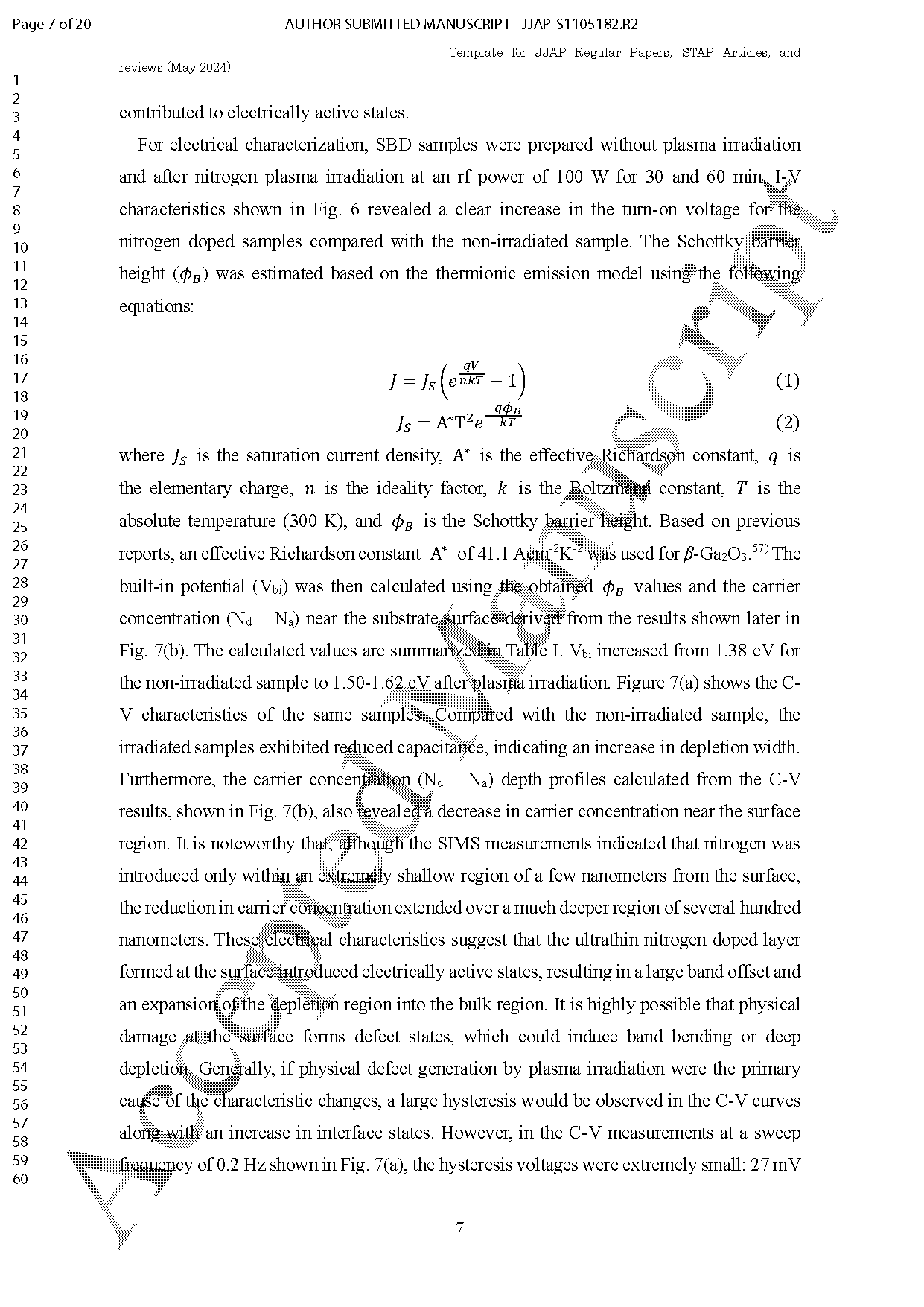
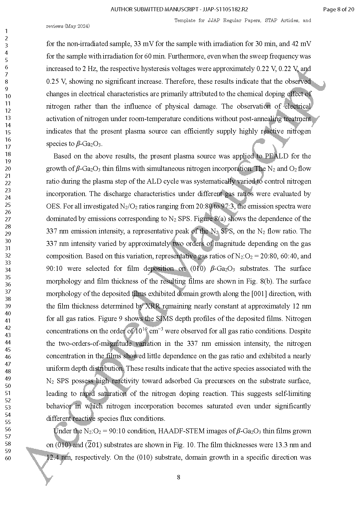
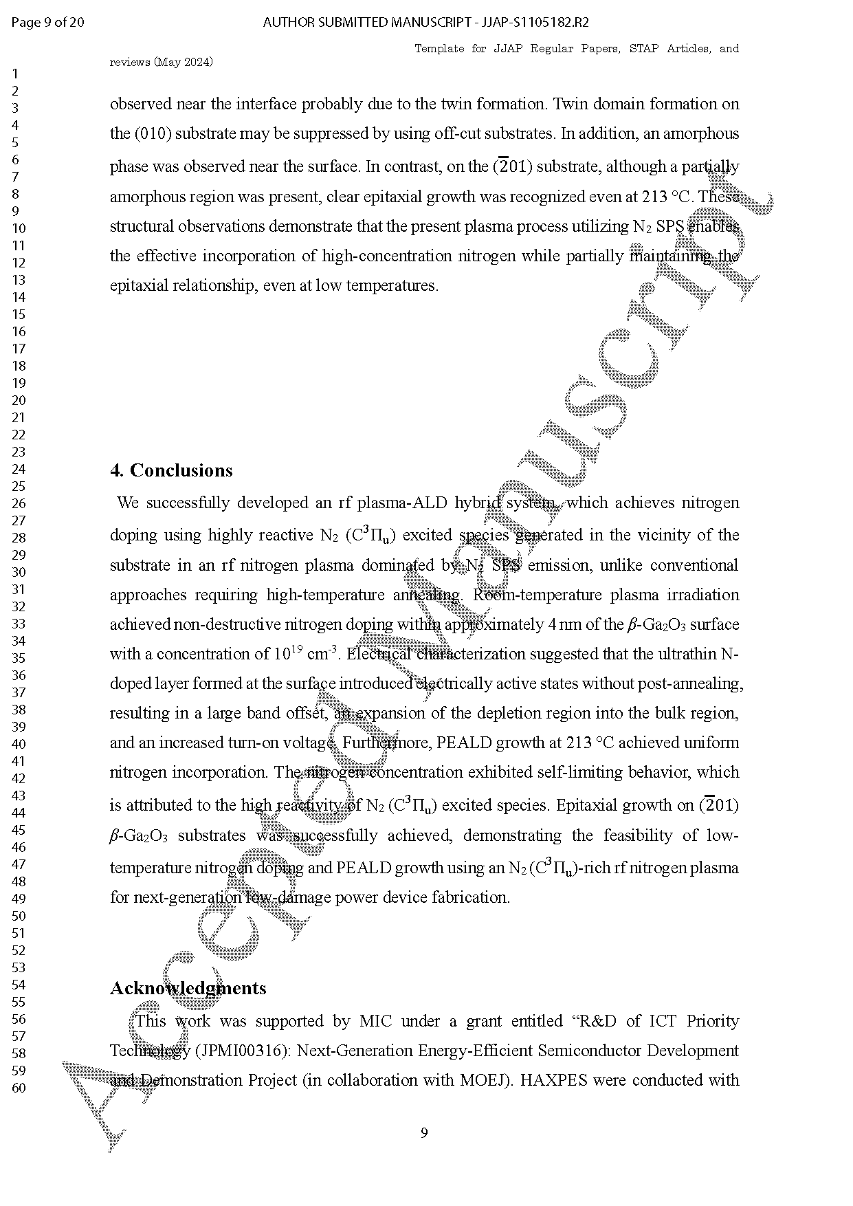
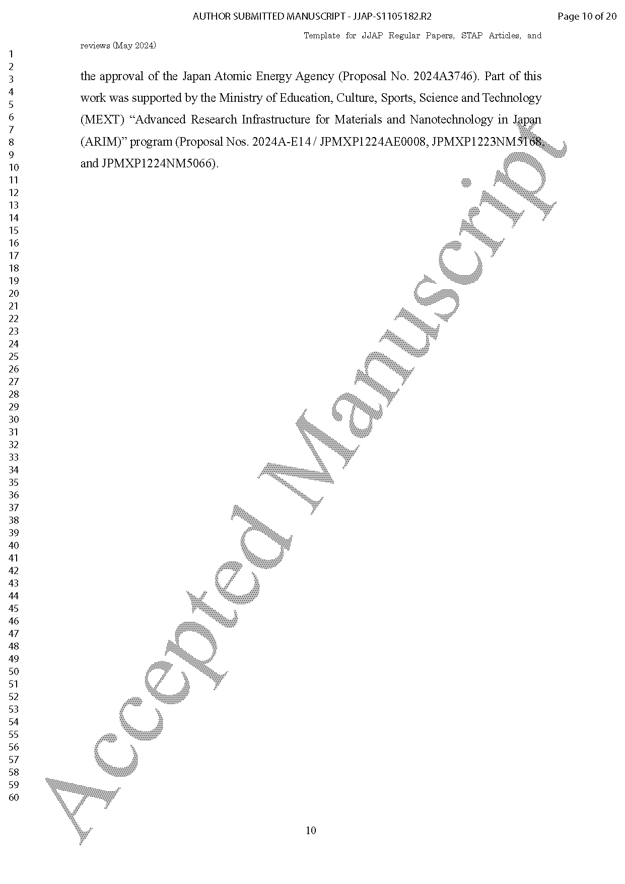
One of the major challenges for β-Ga2O3, a wide-bandgap semiconductor, is the realization of effective nitrogen doping. In this study, we propose a low-thermal-budget nitridation process utilizing molecularly excited nitrogen species, N2 (C3Πu), corresponding to the N2 Second Positive System, whose emission is dominantly observed in nitrogen plasma. We successfully generated N2 (C3Πu) excited species in an rf nitrogen plasma, although such species are predominantly observed in atmospheric-pressure non-equilibrium plasmas. Using this rf nitrogen plasma, we investigated low-temperature nitrogen doping for β-Ga2O3 substrates as well as plasma-enhanced atomic layer deposition (PEALD) growth of nitrogen-doped β-Ga2O3. Room-temperature plasma irradiation enabled nitrogen incorporation at approximately 1×1019 cm−3 within ~4 nm of the surface. Electrical characterization of Schottky barrier diodes revealed the incorporated nitrogen functions as an electrically active dopant without post annealing. Furthermore, PEALD growth performed at 213 °C enabled uniform nitrogen incorporation on the order of 1019 cm−3.
Highlights
Development of an RF nitrogen plasma dominated by the N₂(C³Πᵤ) excited state, enabling low-temperature N-doping of β-Ga₂O₃.
Achievement of room-temperature, high-concentration, low-damage surface N-doping.
Demonstration that the introduced N forms Ga–N chemical bonds and exhibits electrical activity.
This nitrogen plasma was further applied to PEALD to enable the growth of β-Ga₂O₃films with low-temperature nitrogen doping.
Low-temperature epitaxial growth was achieved, providing a new route for the fabrication of β-Ga₂O₃ devices with a low thermal budget.
Conclusions
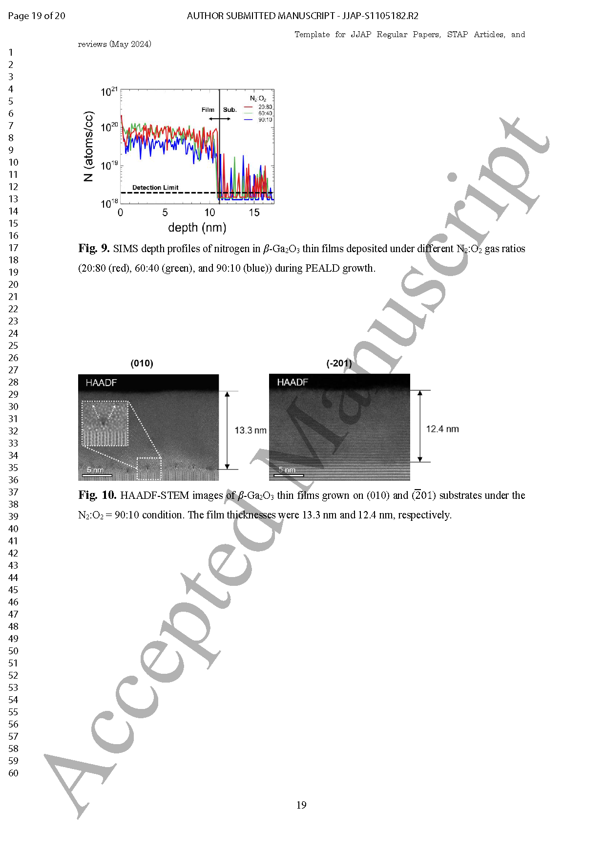
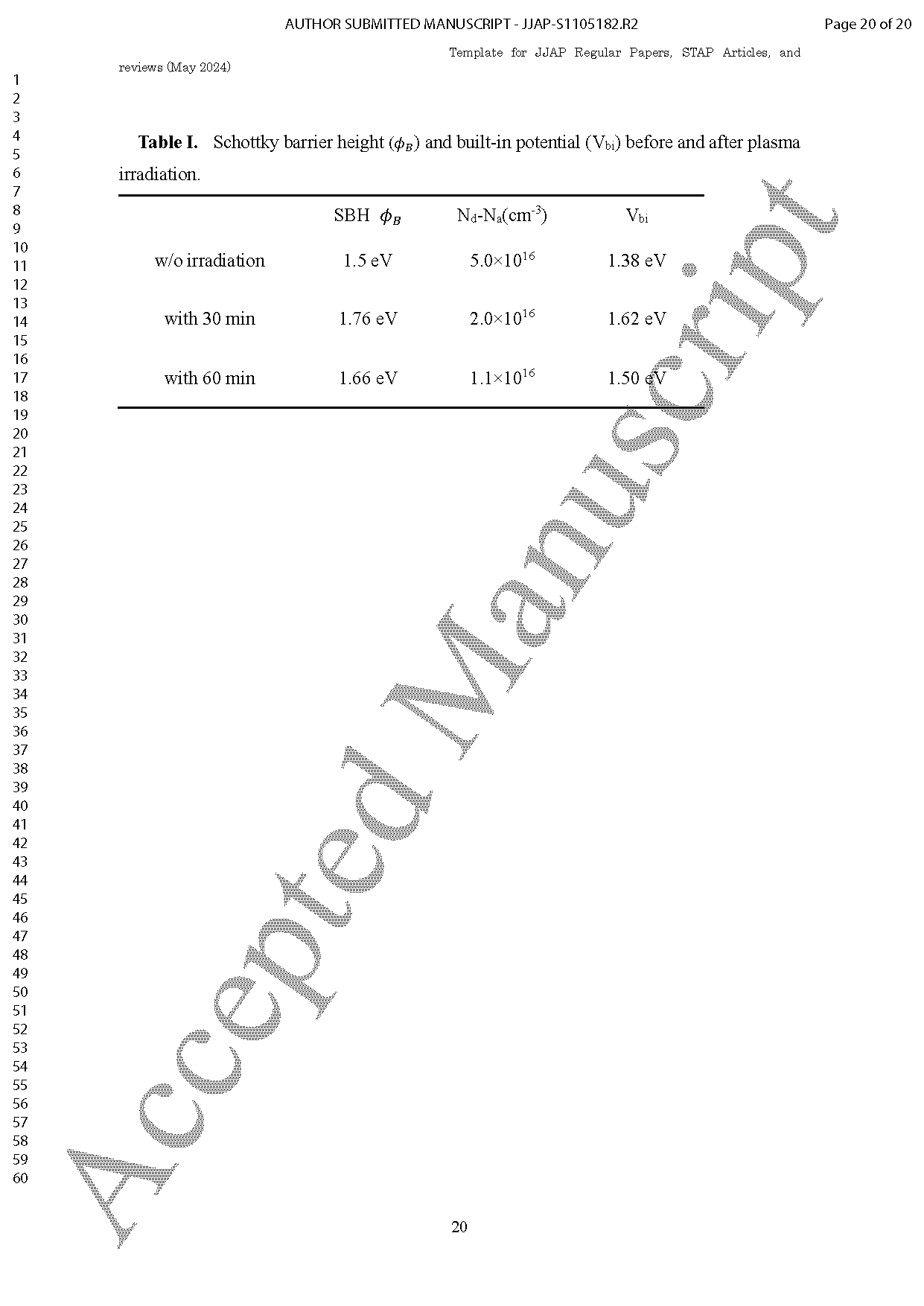
We successfully developed an rf plasma-ALD hybrid system, which achieves nitrogen doping using highly reactive N₂ (C³Πᵤ) excited species generated in the vicinity of the substrate in an rf nitrogen plasma dominated by N2 SPS emission, unlike conventional approaches requiring high-temperature annealing. Room-temperature plasma irradiation achieved non-destructive nitrogen doping within approximately 4 nm of the β-Ga2O3 surface with a concentration of 1019 cm−3. Electrical characterization suggested that the ultrathin N-doped layer formed at the surface introduced electrically active states without post-annealing, resulting in a large band offset, an expansion of the depletion region into the bulk region, and an increased turn-on voltage. Furthermore, PEALD growth at 213 °C achieved uniform nitrogen incorporation. The nitrogen concentration exhibited self-limiting behavior, which is attributed to the high reactivity of N₂ (C³Πᵤ) excited species. Epitaxial growth on (-201) β-Ga2O3 substrates was successfully achieved, demonstrating the feasibility of low-temperature nitrogen doping and PEALD growth using an N₂ (C³Πᵤ)-rich rf nitrogen plasma for next-generation low-damage power device fabrication.
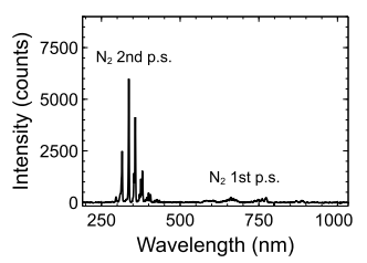
Fig. 1. Optical emission spectroscopy (OES) spectrum of the rf nitrogen plasma measured at a pressure of 250 Pa and an rf power of 100 W.
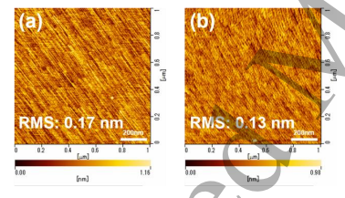
Fig. 2. AFM images of the (010, β-Ga2O3 substrate surfaces (a, before and (b, after 30 min rf nitrogen plasma irradiation at an rf power of 100 W.
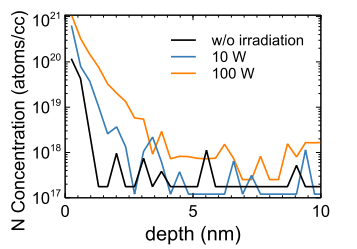
Fig. 3. Nitrogen depth profiles obtained by SIMS measurements for β-Ga2O3 samples without plasma irradiation (black) and after rf nitrogen plasma irradiation at rf powers of 10 (blue, and 100 W (orange) for 30 min.
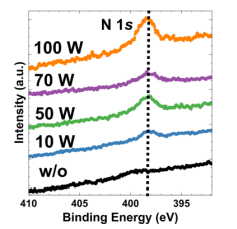
Fig. 4. N 1s XPS spectra of β-Ga2O3 substrates without plasma irradiation (black, after 30 min rf nitrogen plasma irradiation at rf powers of 10 (blue), 50 (green), 70 (purple), and 100 W (orange).
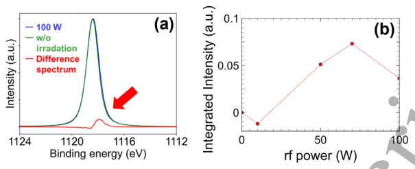
Fig. 5. (a) Ga 2p XPS spectra of the β-Ga2O3 substrate before plasma irradiation (green) and after rf nitrogen plasma irradiation at 100 W for 30 min (blue). The difference spectrum is shown in red. (b) Change in the integrated intensity of the difference spectra as a function of rf power.
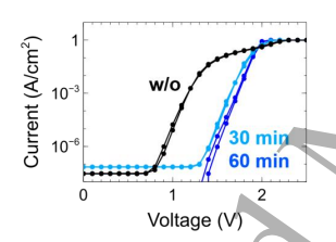
Fig. 6. I-V characteristics of Pt SBDs fabricated on β-Ga2O3 substrates without plasma irradiation (black) and after rf nitrogen plasma irradiation at 100 W for 30 (cyan) and 60 min (blue).
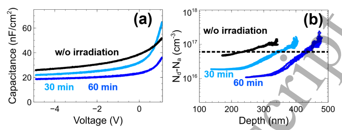
Fig. 7. (a) C-V characteristics of Pt SBDs fabricated on β-Ga2O3 substrates without plasma irradiation (black) and after rf nitrogen plasma irradiation at 100 W for 30 (cyan) and 60 min (blue). (b) Carrier concentration (Nd − Na) depth profiles calculated from the C-V measurements.
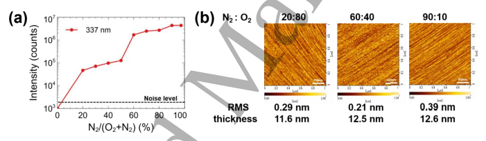
Fig. 8. (a) Dependence of the 337 nm emission intensity on the N2:O2 flow ratio. (b) AFM images of β-Ga2O3 thin films deposited under different N2:O2 ratios, together with the corresponding RMS surface roughness and film thickness determined from XRR measurements.
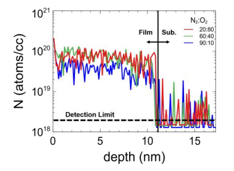
Fig. 9. SIMS depth profiles of nitrogen in β-Ga2O3 thin films deposited under different N2:O2 gas ratios (20:80 (red), 60:40 (green), and 90:10 (blue)) during PEALD growth.
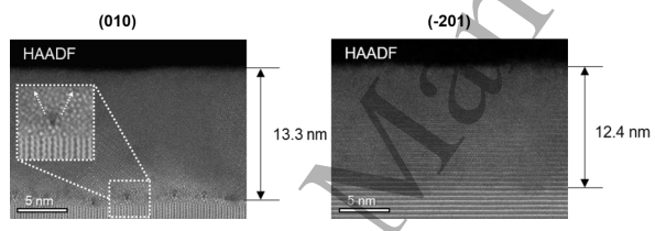
Fig. 10. HAADF-STEM images of β-Ga2O3 thin films grown on (010) and (-201) substrates under the N2:O2 = 90:10 condition. The film thicknesses were 13.3 nm and 12.4 nm, respectively.
DOI:
doi.org/10.35848/1347-4065/aea0da
Instruction
Official Account

Cooperation
Top
