



A research team led by Professor Wang Qianjin and Senior Experimentalist Tan Qiuhong from Yunnan Normal University, and Researcher Liu Zeng from Inner Mongolia University published an article titled "Dual-Band Photodetection and Interfacial Carrier Dynamics of CuInP₂S₆/Ga₂O₃ Van der Waals Heterojunction for Neuromorphic-Like Recognition and Optical Communication" in the academic journal Laser & Photonics Reviews.
Abstract
A dual-band device that can simultaneously possess high sensitivity and neuron-like processing capabilities is highly desirable for next-generation intelligent optoelectronic systems. However, traditional single-material devices have the problems of poor performance and low integration level. Furthermore, due to their high-power consumption, they are limited in applications such as integrated sensing, computing and storage, optical encryption communication, and imaging. Here, we report a multifunctional CuInP₂S₆ (CIPS)/Ga₂O₃ heterojunction that integrates ultraviolet (UV–Visible photodetection, artificial synaptic function, neuron- like recognition, and dual-wavelength optical communication and imaging. Notably, this constructed type-II CIPS/Ga₂O₃ van der Waals heterojunction provides an opportunity to modulate the interface charge carrier transport, then enhance the light absorbance, thereby achieving high responsivity (275 A/W), and enhanced detectivity (1.95 ×10¹⁵ Jones) under irradiation of 245 nm UV light. Significantly, the device also exhibits vital synaptic plasticity, including dual-pulse promotion and adjustable memory retention capability. By mapping the experimentally extracted single-device forgetting dynamics to a simulated convolutional neural network framework, high accuracy has been achieved on both simple and complex datasets. Additionally, wavelength-selective light response supports dual-band UV-visible light communication and imaging. This work establishes a multifunctional heterojunction platform, advancing the research and development of modern optoelectronics.
Highlights
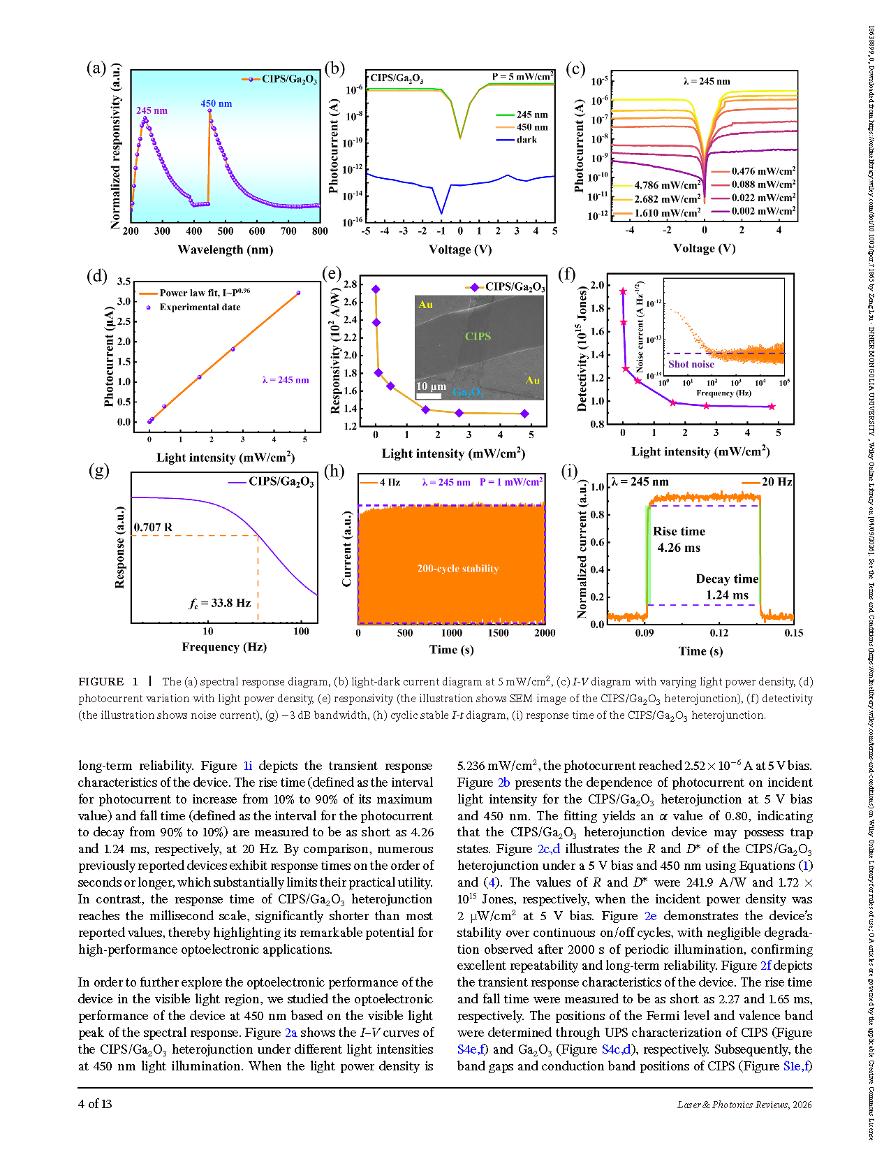
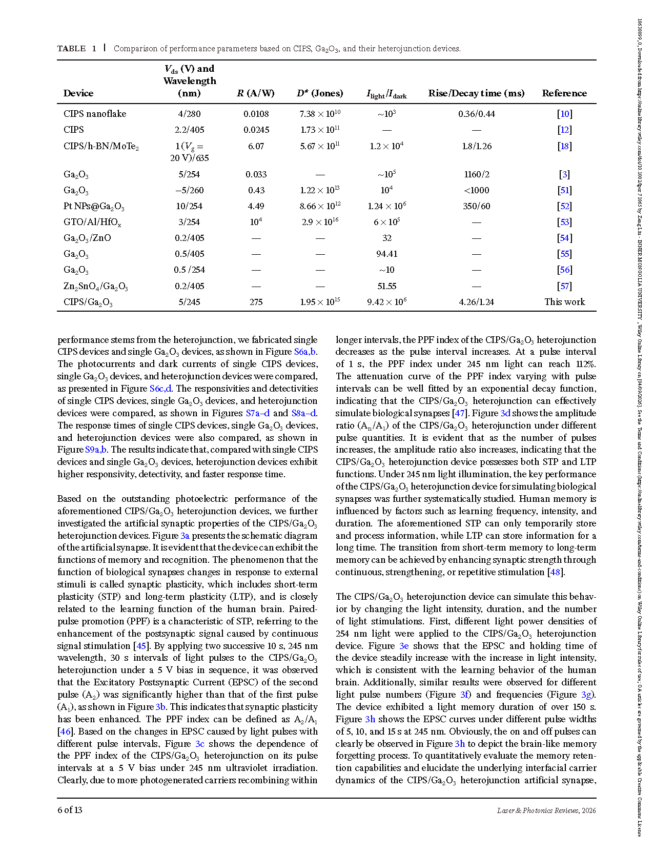
Photo-to-dark current ratio, responsivity, and detectivity are ~9.42×10⁶, 275 A/W, 1.95×10¹⁵Jones, respectively. Single CIPS or Ga₂O₃devices often fail to achieve effective separation of photogenerated carriers, have low carrier mobility, and have a fixed energy band structure, which limit their application value. By taking advantage of the tunable bandgap of CIPS, a type-II band structure was successfully constructed, which can effectively solve a series of problems. The research results show that this design not only achieves a highly sensitive device but also provides a guarantee for the application of the device.
Ultraviolet-visible dual-band encryption communication and imaging applications. Based on the excellent photoelectric performance of the aforementioned heterojunction devices, by utilizing the optimal response bands of Ga₂O₃and CIPS, dual-band encrypted optical communication and imaging applications have been achieved in the ultraviolet and visible light ranges.
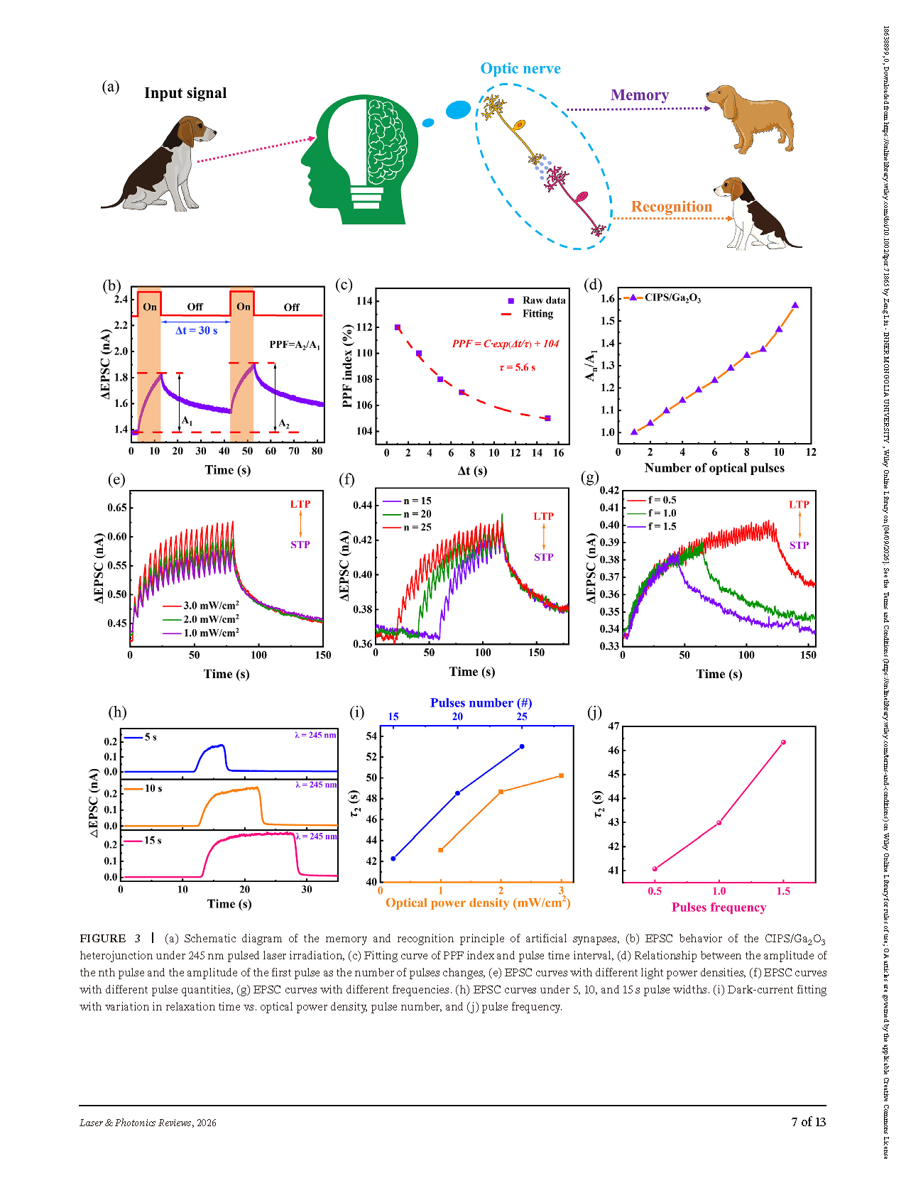
Artificial synapses simulate the high-precision recognition capabilities of human memory and neural networks. By imitating the memory and forgetting functions of humans and utilizing the artificial synapses of heterojunction devices, a neural network architecture was constructed, achieving high-precision recognition. This provided experimental support for modern low-power, high-integration, and high-sensitivity devices.
Conclusion
In summary, we have demonstrated a multifunctional CIPS/Ga₂O₃ heterojunction device that integrates high-performance ultraviolet-visible light detection, artificial synaptic behavior, neuromorphic recognition, as well as dual-band optical communication and imaging functionalities onto a single platform. By combining the Ga₂O₃ thin film grown by MOCVD with the mechanically exfoliated CIPS nanosheets through a dry transfer process, a clear and well-defined heterojunction interface was achieved, thereby enabling efficient interface charge modulation. The synergistic effect of the wide bandgap material Ga₂O₃ and the unique type-II band alignment caused by the bandgap tunability of CIPS jointly promoted carrier separation and inhibited recombination phenomena, thus achieving a high responsivity (275 A/W) and improved detectivity (1.95×10¹⁵ Jones) under 245 nm ultraviolet light irradiation. In addition to the optical detection function, the device also exhibits significant synaptic plasticity, including dual-pulse promotion and adjustable memory retention capabilities, which enables the effective simulation of biological synaptic functions. By directly mapping the extracted forgetting characteristics from experiments to the neural network framework, a high accuracy was achieved based on MNIST and CIFAR-10 datasets, demonstrating the feasibility of neuromorphic-like computing. Moreover, the wavelength-selective light response function enables the realization of dual-band ultraviolet-visible light communication and imaging, highlighting the potential of the CIPS/Ga₂O₃ heterojunction in integrated sensing and information transmission. This work provides a feasible strategy for constructing a multifunctional optoelectronic device integrating photodetection, storage, neuromorphic- like processing functions, communication, and imaging, opening up new opportunities for intelligent optoelectronic and neuromorphic-like vision systems.
Project Support
This work was supported by the National Natural Science Foundation of China (Nos. 62464014, 12464025, 12264056, 62564011 and 62204125), the Young Scientists Fund (Type A) of the Natural Science Foundation of Inner Mongolia Autonomous Region of China (2026QA016), the Basic Research Program of Yunnan Province (No. 202401AT070134), Project for Building a Science and Technology Innovation Center Facing South Asia and Southeast Asia (202403AP140015), Spring City Plan: The High-level Talent Promotion and Training Project of Kunming (2022SCP005), the Basic Scientific Research Funding for Universities Directly Affiliated with the Inner Mongolia Autonomous Region of China (Grant No. 2026JBKY002), and Yunnan Provincial Department of Education Scientific Research Fund Project (No. 2026Y0319).
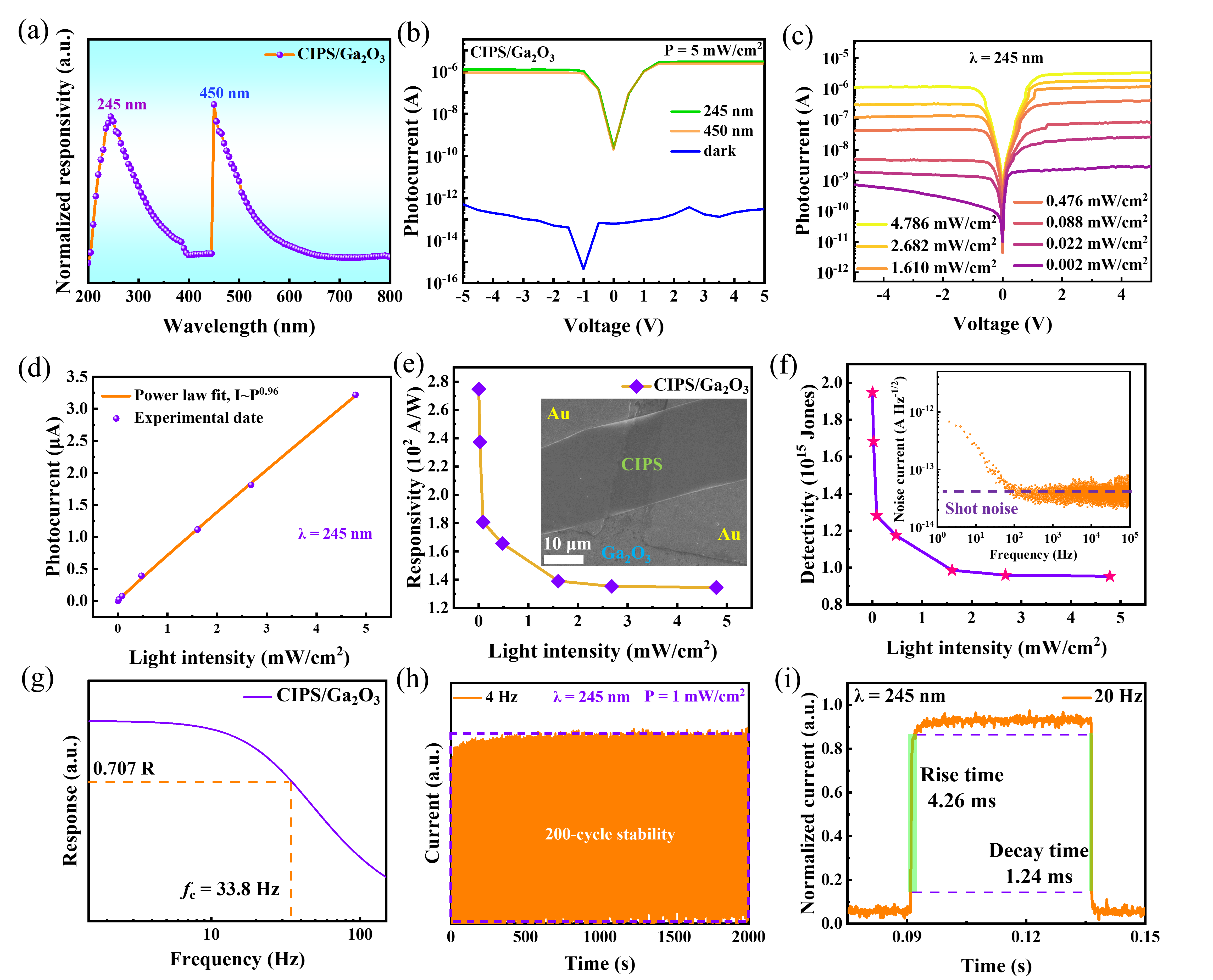
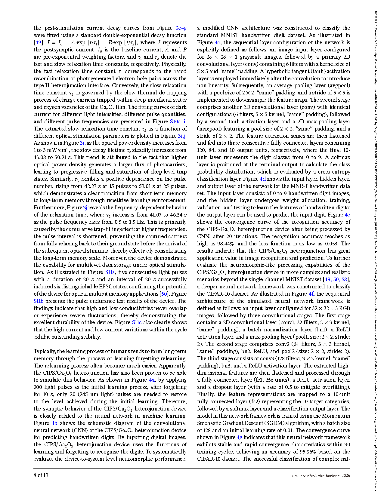
Figure 1. The (a) spectral response diagram, (b) light-dark current diagram at 5 mW/cm2, (c) I-V diagram with varying light power density, (d) photocurrent variation with light power density, (e) responsivity (the illustration shows SEM image of the CIPS/Ga₂O₃ heterojunction), (f) detectivity (the illustration shows noise current), (g) -3 dB bandwidth, (h) cyclic stable I-t diagram, (i) response time of the CIPS/Ga₂O₃ heterojunction.
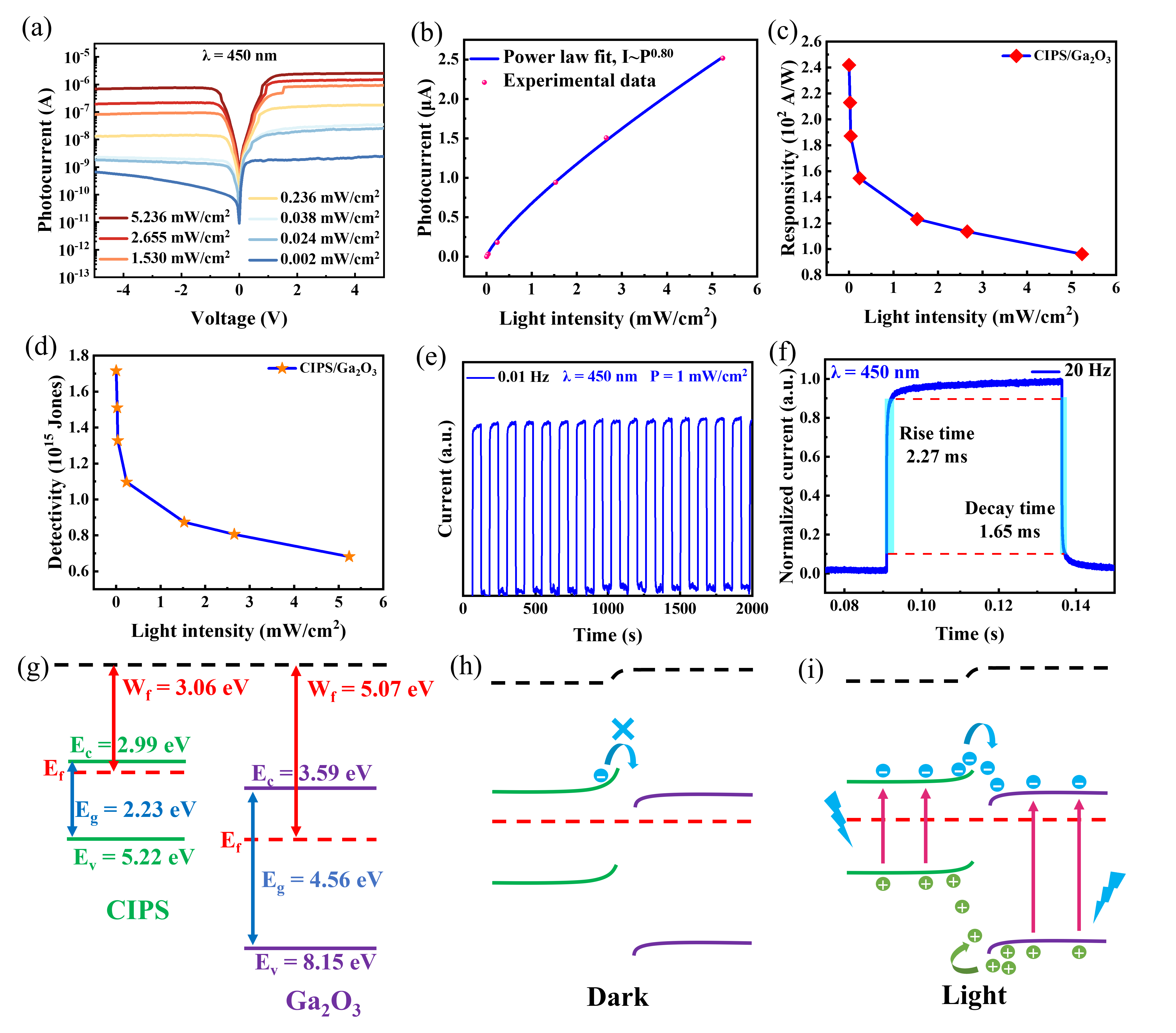
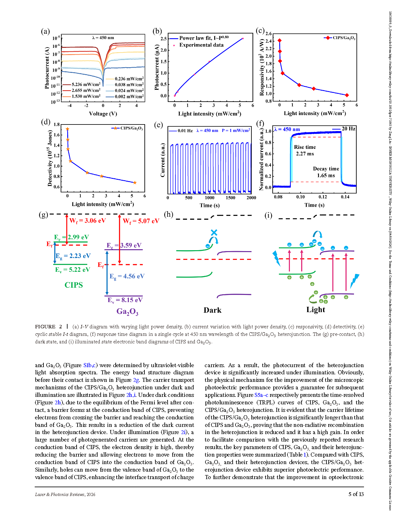
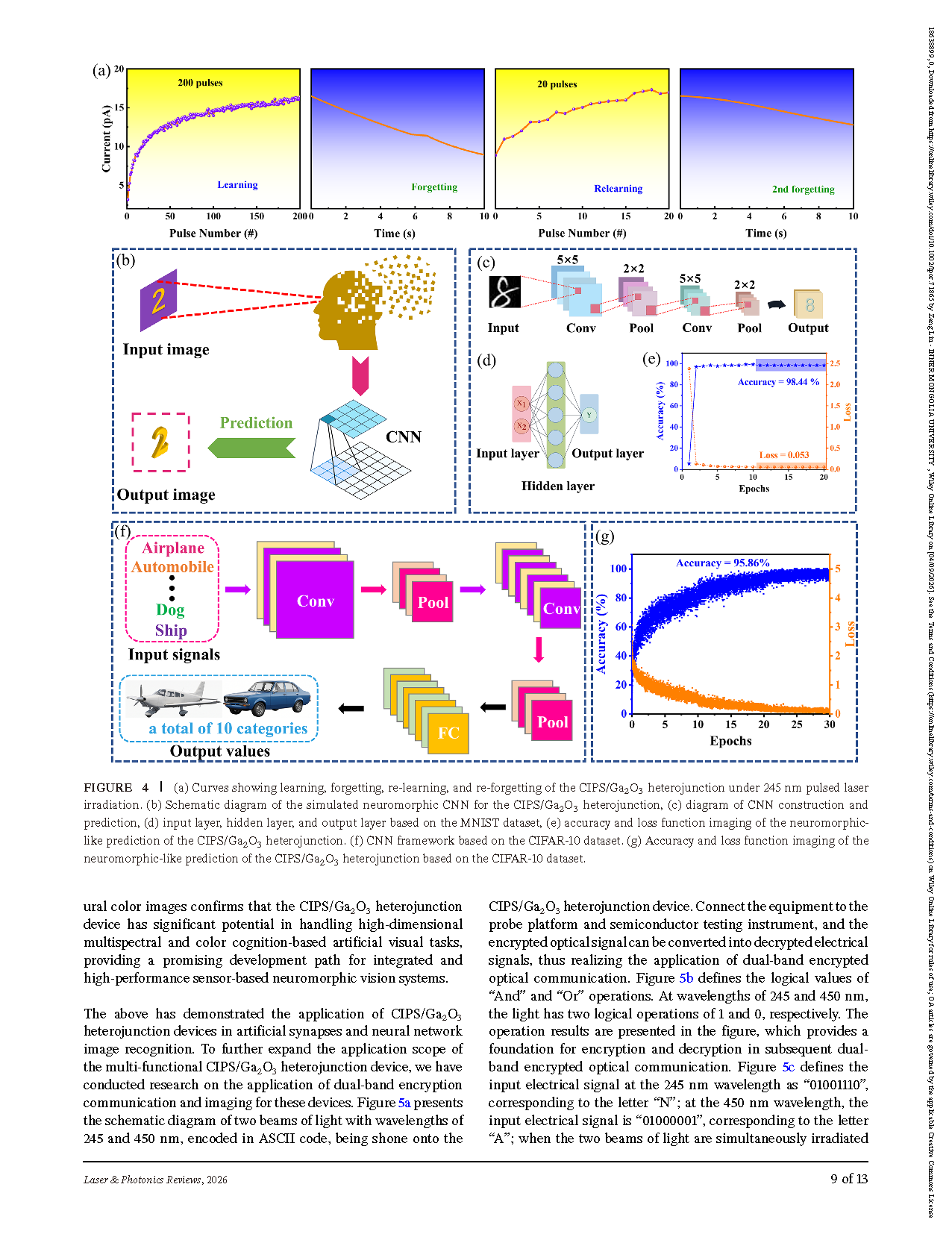
Figure 2. (a) I-V diagram with varying light power density, (b) current variation with light power density, (c) responsivity, (d) detectivity, (e) cyclic stable I-t diagram, (f) response time diagram in a single cycle at 450 nm wavelength of the CIPS/Ga₂O₃ heterojunction. The (g) pre-contact, (h) dark state and (i) illuminated state electronic band diagrams of CIPS and Ga₂O₃.
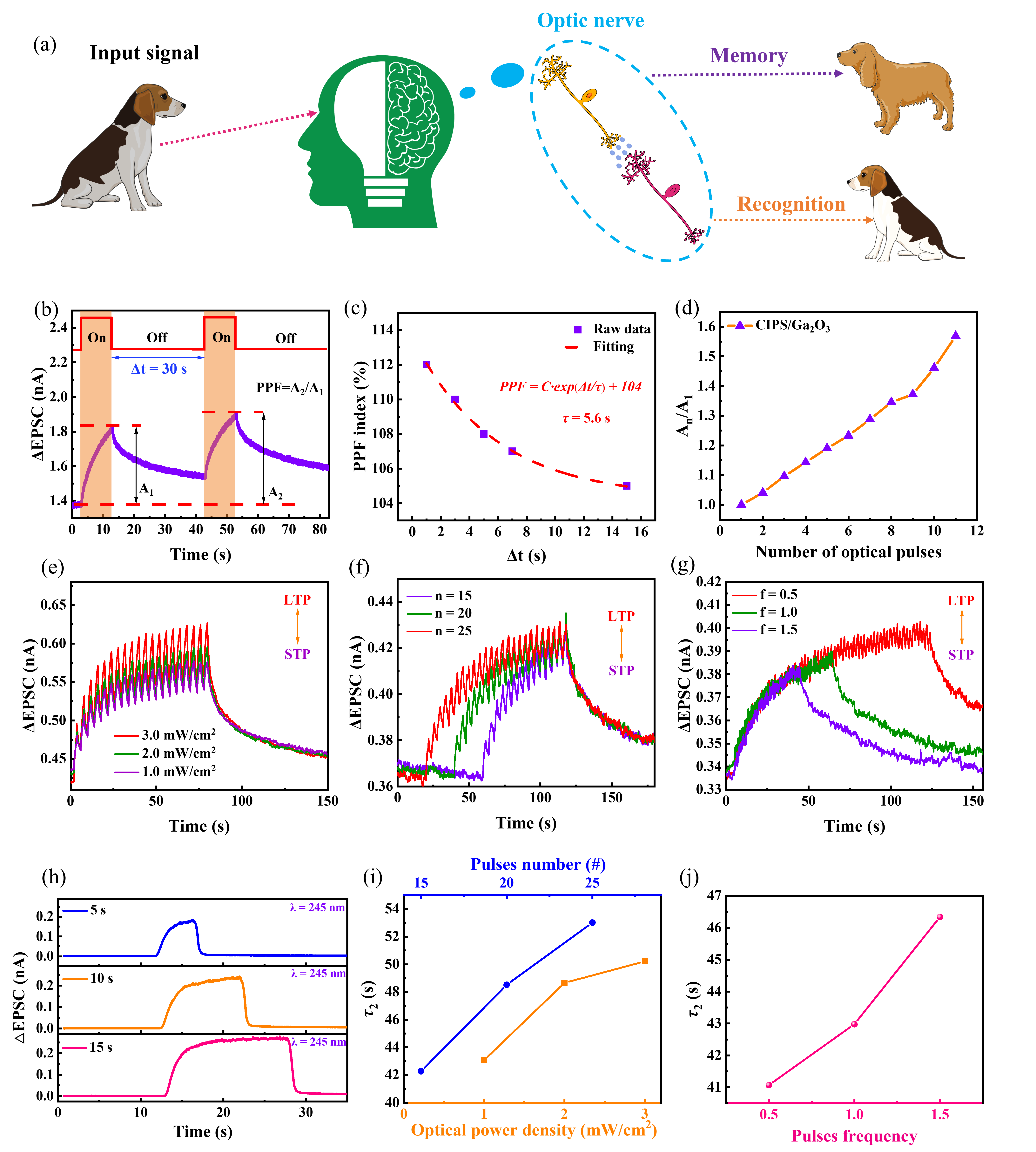
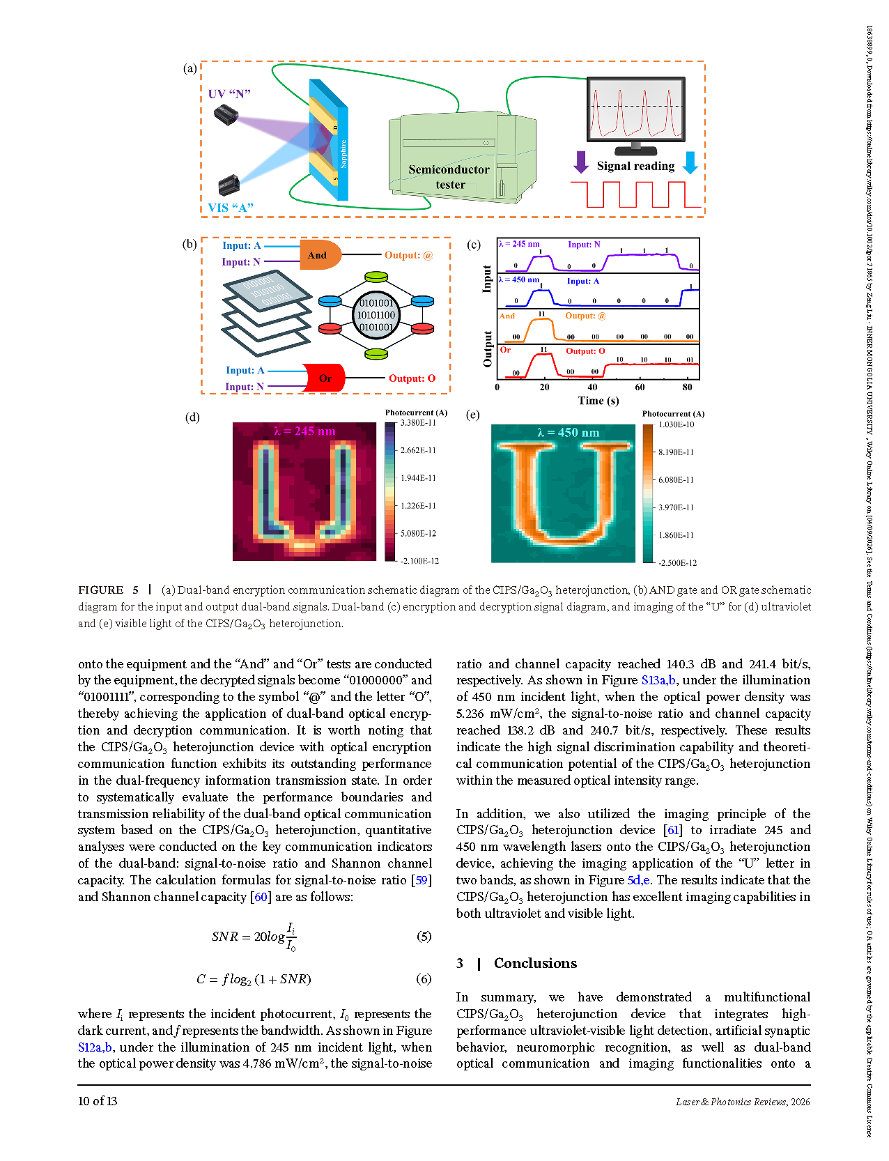
Figure 3. (a) Schematic diagram of the memory and recognition principle of artificial synapses, (b) EPSC behavior of the CIPS/Ga₂O₃ heterojunction under 245 nm pulsed laser irradiation, (c) Fitting curve of PPF index and pulse time interval, (d) Relationship between the amplitude of the nth pulse and the amplitude of the first pulse as the number of pulses changes, (e) EPSC curves with different light power densities, (f) EPSC curves with different pulse quantities, (g) EPSC curves with different frequencies. (h) EPSC curves under 5 s, 10 s and 15 s pulse widths. (i) Dark-current fitting with variation in relaxation time vs. optical power density, pulses number and (j) pulses frequency.
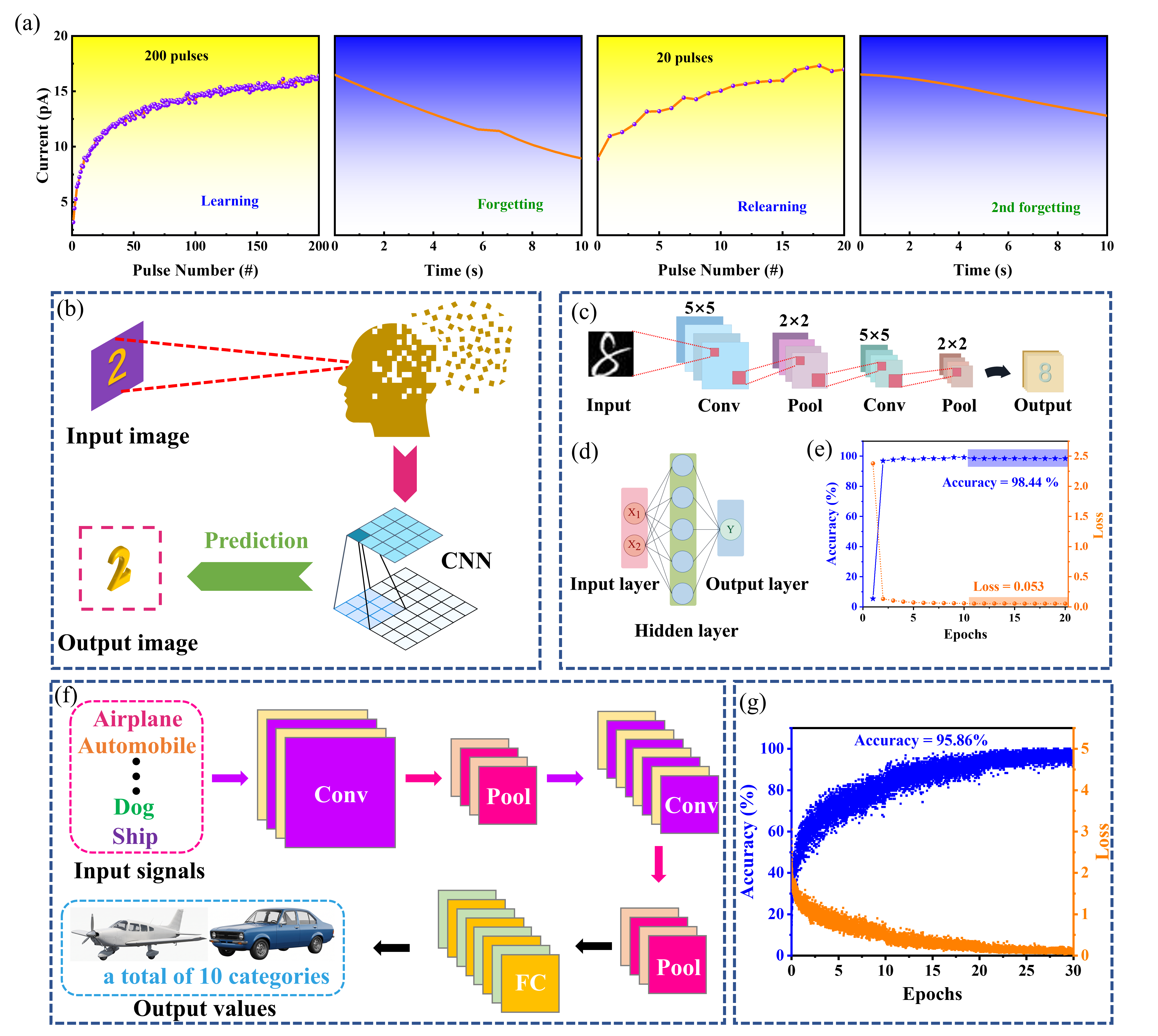
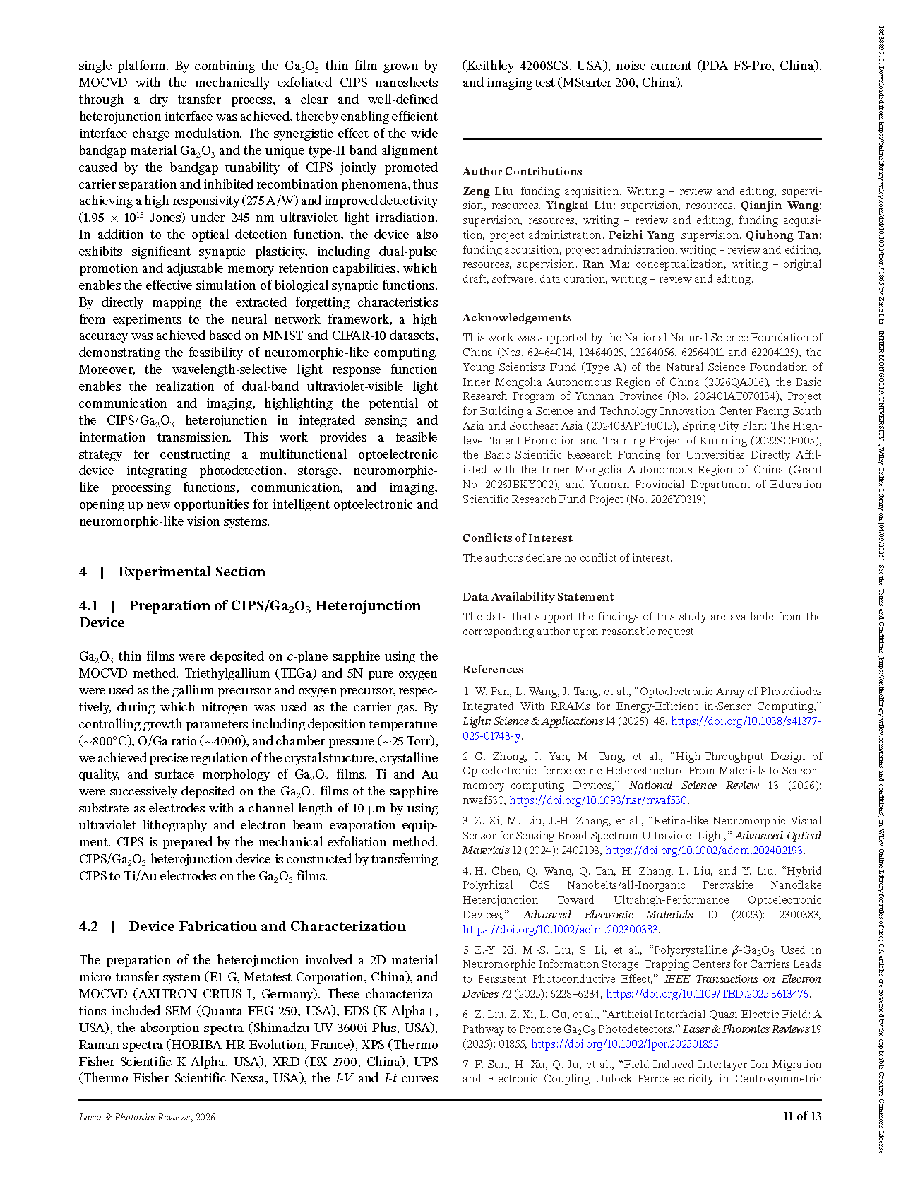
Figure 4. (a) Curves showing learning, forgetting, re-learning, and re-forgetting of the CIPS/Ga₂O₃ heterojunction under 245 nm pulsed laser irradiation. (b) Schematic diagram of the simulated neuromorphic CNN for the CIPS/Ga₂O₃ heterojunction, (c) diagram of CNN construction and prediction, (d) input layer, hidden layer and output layer based on the MNIST dataset, (e) accuracy and loss function imaging of the neuromorphic-like prediction of the CIPS/Ga₂O₃ heterojunction. (f) CNN framework based on the CIFAR-10 dataset. (g) Accuracy and loss function imaging of the neuromorphic-like prediction of the CIPS/Ga₂O₃ heterojunction based on the CIFAR-10 dataset.
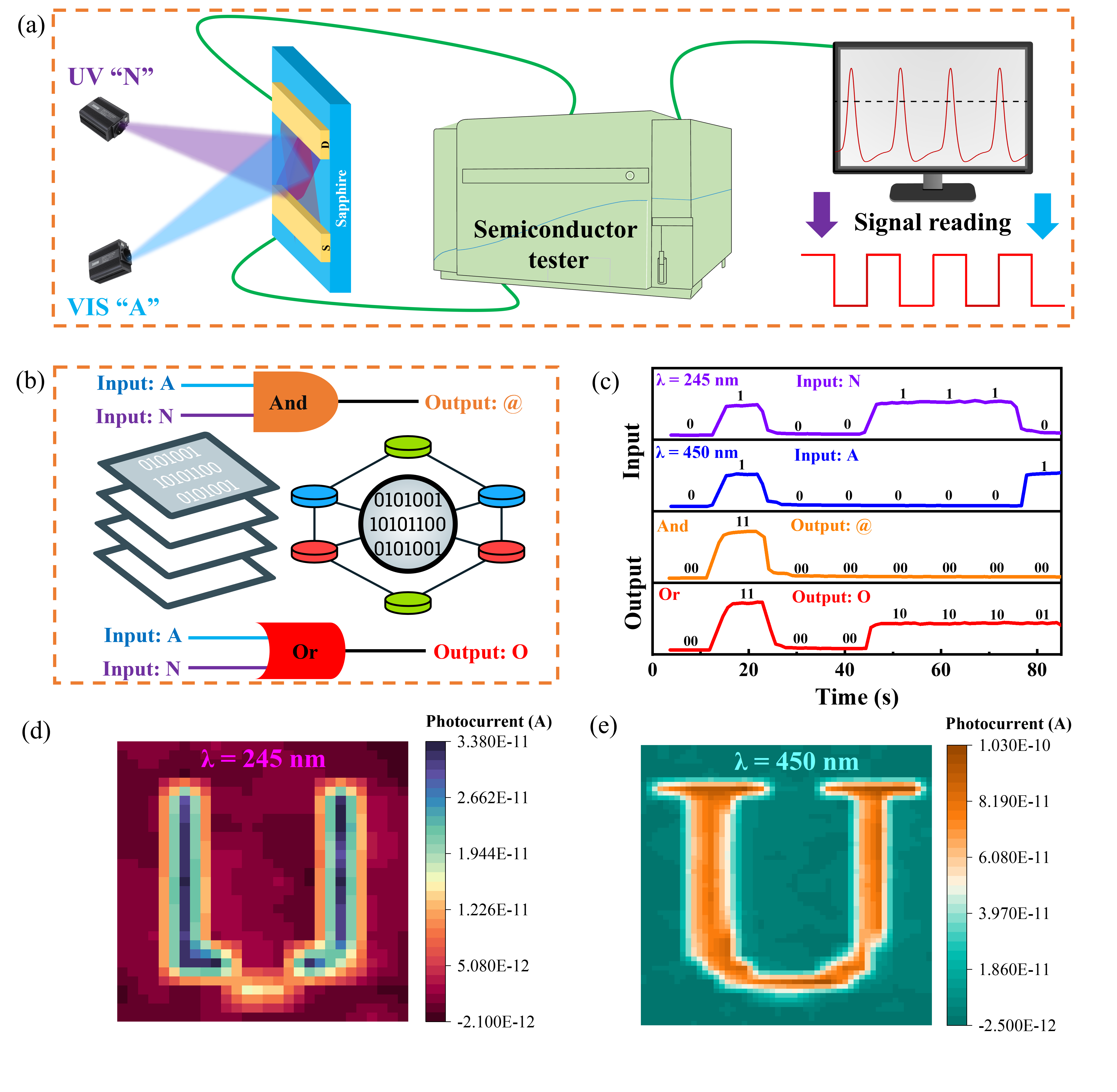
Figure 5. The (a) dual-band encryption communication schematic diagram of the CIPS/Ga₂O₃ heterojunction, (b) And gate and Or gate schematic diagram for the input and output dual-band signals. Dual-band (c) encryption and decryption signal diagram, and imaging of the "U" for (d) ultraviolet and (e) visible light of the CIPS/Ga₂O₃ heterojunction.
DOI:
doi.org/10.1002/lpor.71865
Instruction
Official Account

Cooperation
Top
