


Researchers from the Ningbo Institute of Materials Technology and Engineering, Chinese Academy of Sciences have published a dissertation titled "A deep ultraviolet photodetector based on n-ε-Ga₂O₃/p-diamond heterojunction" in Applied Surface Science.
Background
Deep-ultraviolet (DUV) detectors have significant potential applications in fields such as optical communications, environmental monitoring, and military early warning systems. Diamond, with an ultra-wide bandgap of 5.47 eV, exhibits intrinsic DUV photoresponse characteristics, coupled with an exceptional high thermal conductivity of 2200 W/m·K and fantastic electrical properties. Compared to conventional Si DUV detectors, the wide bandgap of diamond promises low solar-blind background noise for DUV detection. However, the difficulty in achieving n-type doping severely restricts its application in bipolar device architectures. As another ultra-wide bandgap semiconductor, Ga2O3 possesses a bandgap of 4.8 eV, and a breakdown field strength of up to 8 MV/cm. In contrast to diamond, Ga2O3 exhibits excellent n-type doping capability while lack effective p-type doping ability. Considering the doping complementary, the combination of diamond and Ga2O3 will pave a new way for the integration of Ga2O3 on diamond, and the fabrication of bipolar devices. Nevertheless, the current integrated fabrication processes for n-type gallium oxide and p-type diamond remain insufficiently developed.
Abstract
Diamond-based deep-ultraviolet photodetectors have significant potential in communications, sensing, and imaging. However, the challenge of n-type doping restricts the fabrication of diamond pn structural photodetectors. In this work, a photodetector based on n-ɛ-Ga2O3/p-diamond heterojunction was fabricated by depositing n-type ɛ-Ga2O3 on p-type diamond substrate via pulsed laser deposition (PLD). X-ray photoelectron spectroscopy (XPS) analysis indicated the ɛ-Ga2O3/diamond heterojunction possesses a Type II band structure, with valence and conduction band offsets of approximately 2.23 eV and 3.10 eV, respectively. The fabricated detector exhibits an ultra-low dark current of 1.16 × 10⁻¹² A and a high photo-to-dark current ratio (PDCR) of 106. The detector also showed excellent spectral selectivity in the deep-ultraviolet range. Moreover, the detector exhibits self-powered operation under DUV illumination because of the built-in electric field at the hetero p-n junction. This study demonstrates the feasibility of integrating ɛ-Ga2O3 with diamond and provides guidance for designing future deep-ultraviolet photodetectors based on ɛ-Ga2O3/diamond heterojunctions.
Highlights
ε-Ga2O3/p-diamond heterojunction:n-type ε-Ga2O3film was deposited on p-type diamond substrate, and a deep ultraviolet photodetector was fabricated based on this hetero pn junction.
Type-II Band Alignment: Precise interfacial engineering achieved a staggered band offset, with valence band (VBO) and conduction band (CBO) offsets of 2.23 eV and 3.10 eV, respectively.
Ultralow Dark Current: The device demonstrated exceptional noise suppression, exhibiting a dark current as low as 1.16×10⁻¹²A and a high light-to-dark current ratio of 106.
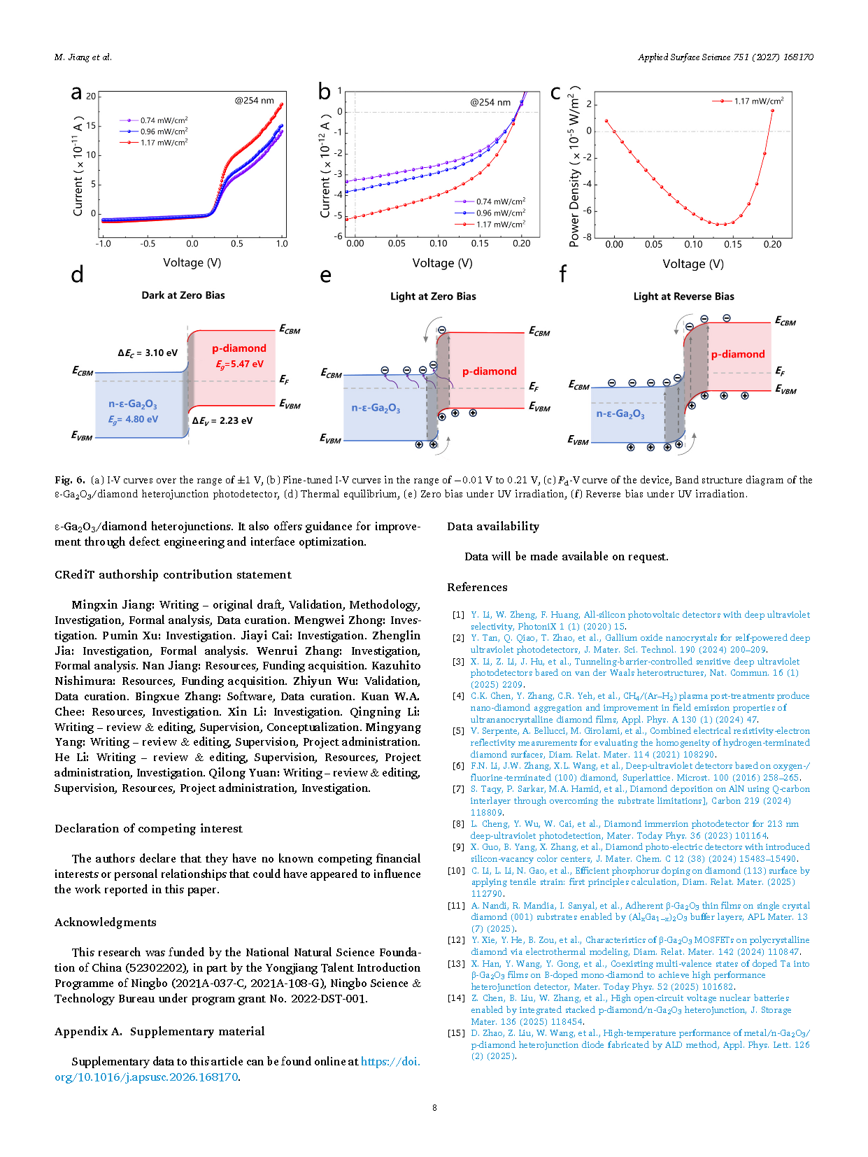
Self-Powered Capability: The photodetector operates autonomously, delivering a short-circuit current (ISC) of 5.04×10⁻¹² A and an open-circuit voltage (VOC) of 0.19 V.
Conclusion
In this study, a DUV photodetector based on anε-Ga2O3/diamond heterojunction was fabricated by depositing n-type ε-Ga2O3 on a p-type diamond substrate. The band structure of the n-ε-Ga2O3/p-diamond heterojunction was determined to be a staggered type (Type II), with VBO and CBO values of 2.23 eV and 3.10 eV, respectively. The fabricated detector features an ultra-low dark current of 1.16 × 10⁻¹² A (at −3 V) and an ultra-high light-to-dark current ratio of 106, with responsivity and specific detection sensitivity of 7.79×10⁻³ A/W and 1.61×10¹² Jones, respectively. Meanwhile, the detector also showed self-power ability, with the open-circuit voltage (VOC) of 0.19 V, short current (ISC) of 5.04×10⁻¹² A, and maximum output power density of 0.69 W/cm2. Structural and interface defects (grain boundaries, twins, dislocations, oxygen vacancies, Ga+ defects) exist in the ε-Ga2O3 film. These defects increase recombination and weaken the built in field via Fermi-level pinning. Thus, breakdown voltage (4.75–7.25 V) and VOC (≈0.19 V) are low. Still, this study shows the feasibility of epitaxial ε-Ga2O3/diamond heterojunctions. It also offers guidance for improvement through defect engineering and interface optimization.
Project Support
This research was funded by the National Natural Science Foundation of China (52302202), in part by the Yongjiang Talent Introduction Programme of Ningbo (2021A-037-C, 2021A-108-G), Ningbo Science & Technology Bureau under program grant No. 2022-DST-001.
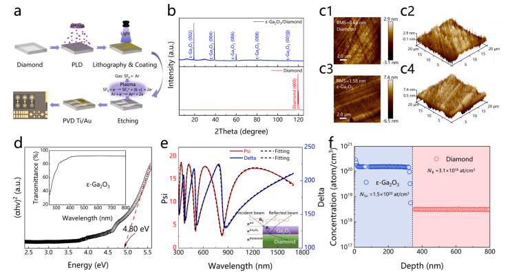
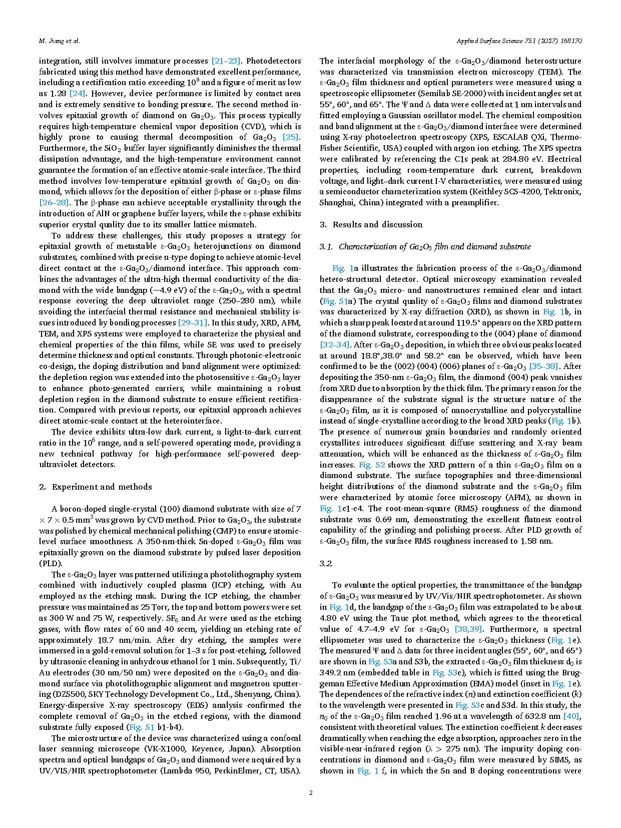
Fig. 1. (a) Schematic of the ε-Ga2O3 PLD growth on diamond substrate and device fabrication process, (b) XRD patterns of ε-Ga2O3 and diamond, 2D and 3D AFM images and roughness profiles for (c1-c2) diamond and (c3-c4) ε-Ga2O3 grown on diamond, scan area 20×20 µm2, (d) UV/Vis/NIR spectra of ε-Ga2O3, (e) Plots of Ψ and Δ ellipsometric angles as functions of wavelength, the inset shows the SE measurement model for the heterostructure, (f) Doping concentrations of ε-Ga2O3 and diamond.

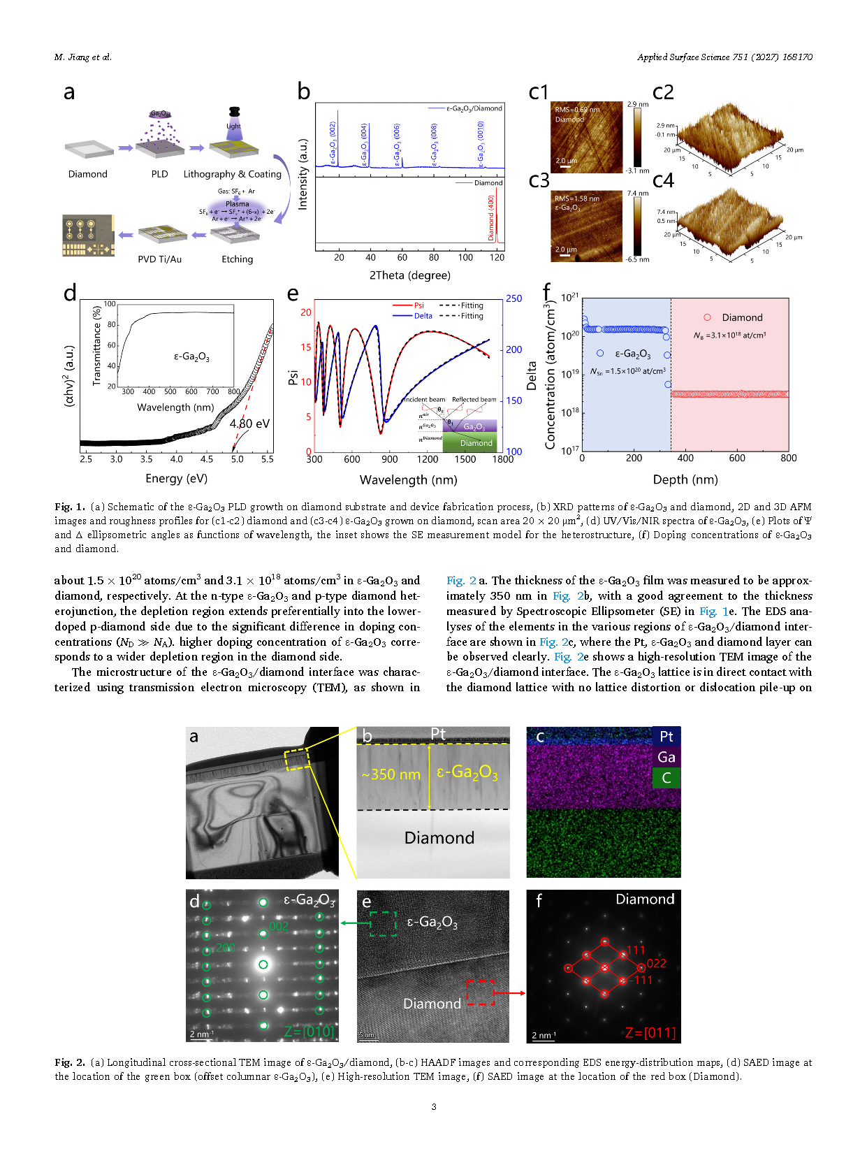
Fig. 2. (a) Longitudinal cross-sectional TEM image of ε-Ga2O3/diamond, (b-c) HAADF images and corresponding EDS energy-distribution maps, (d) SAED image at the location of the green box (offset columnar ε-Ga2O3), (e) High-resolution TEM image, (f) SAED image at the location of the red box (Diamond).
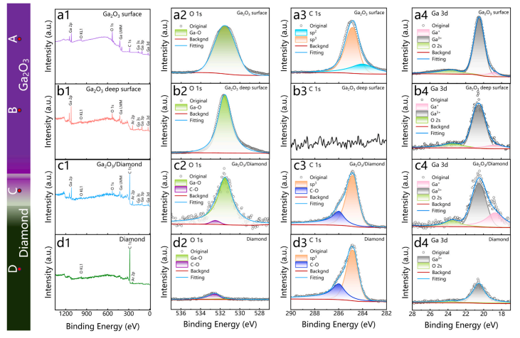
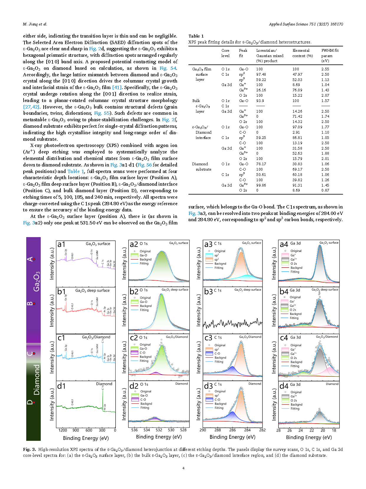
Fig. 3. High-resolution XPS spectra of the ε-Ga2O3/diamond heterojunction at different etching depths. The panels display the survey scans, O 1s, C 1s, and Ga 3d core-level spectra for: (a) the ε-Ga2O3 surface layer, (b) the bulk ε-Ga2O3 layer, (c) the ε-Ga2O3/diamond interface region, and (d) the diamond substrate.
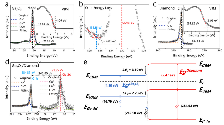
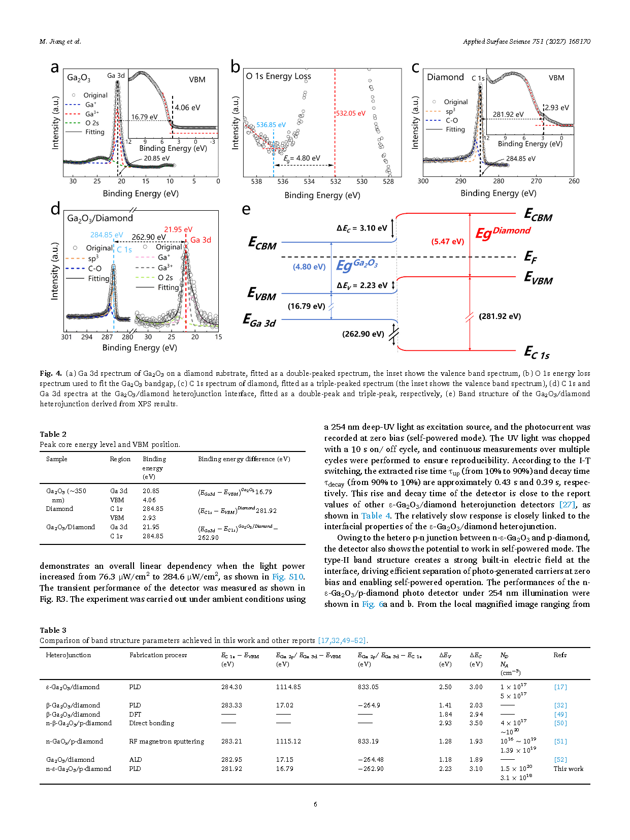
Fig. 4. (a) Ga 3d spectrum of Ga₂O₃ on a diamond substrate, fitted as a double-peaked spectrum, the inset shows the valence band spectrum, (b) O 1s energy loss spectrum used to fit the Ga₂O₃ bandgap, (c) C 1s spectrum of diamond, fitted as a triple-peaked spectrum (the inset shows the valence band spectrum), (d) C 1s and Ga 3d spectra at the Ga₂O₃/diamond heterojunction interface, fitted as a double-peak and triple-peak, respectively, (e) Band structure of the Ga₂O₃/diamond heterojunction derived from XPS results.
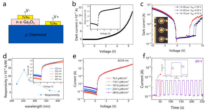
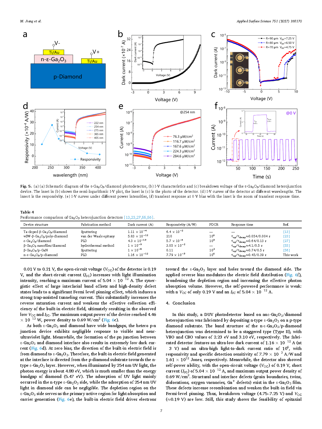
Fig. 5. (a) (a) Schematic diagram of the ε-Ga₂O₃/diamond photodetector, (b) I-V characteristics and (c) breakdown voltage of the ε-Ga₂O₃/diamond heterojunction device. The inset in (b) shows the semi-logarithmic I-V plot, the inset in (c) is the photo of the detector. (d) I-V curves of the detector at different wavelengths. The insert is the responsivity. (e) I-V curves under different power intensities, (f) transient response at 0 V bias with the inset is the zoom of transient response time.
DOI:
doi.org/10.1016/j.apsusc.2026.168170
Instruction
Official Account

Cooperation
Top
