


Researchers from the Argonne National Laboratory have published a dissertation titled "20 MeV Proton Irradiation of 200μm n-type Gallium Oxide Schottky Diodes " in NAECON 2026 - IEEE National Aerospace and Electronics Conference.
Background
Gallium Oxide (GaO) is a promising material for use in power electronics. With its wide bandgap and high breakdown voltage, it has the potential to provide more efficient and compact power systems. It is of particular interest to aerospace applications, due to the material properties of GaO providing a great degree of radiation tolerance. In addition to power electronics applications, GaO has promising applications in RF applications. In the aerospace and especially the space domain, cosmic radiation is a persistent challenge for electronic devices. This radiation comes in the form of protons, heavy ions, electrons, and neutrons from solar radiation and atmospheric interactions. For any emerging technology to be applied to these domains, their radiation properties must be known. For GaO, several studies have been done on various kinds of radiation, including neutron and proton radiation. These studies exposed devices to radiation and then assessed their material and electrical properties after exposure. There have not been studies that expose these devices to radiation at several doses and assess their properties with biasing in situ.
Abstract
Eight n-type Gallium Oxide (GaO) Schottky diodes were exposed to 100 krad of 20 MeV proton radiation at the ATLAS beamline at Argonne National Laboratory. A custom fixture was developed to allow irradiation of multiple devices in a series in a vacuum chamber with applied biasing. Devices were biased at either 0 V, 2V, or -100 V. Irradiation was divided into eight stages with voltage sweeps done between each stage. One device at -100 V was observed to fail during radiation. Another device was damaged due to being on the same package as the first. Three other devices showed increased leakage current between one to two orders of magnitude above their specifications in post-radiation observation. There was no observed difference between the devices biased at 2 V and those at 0 V.
Highlights
Designed a customized vacuum test fixture capable of mounting multiple Ga₂O₃ Schottky diodes simultaneously, enabling external bias application and current monitoring during irradiation to improve testing efficiency within limited beam time.
Eight n-type Ga₂O₃ Schottky diodes, each with a 200 μm thick substrate and 10 μm epitaxial layer, were cumulatively exposed to approximately 100 krad of irradiation, with biases of 0 V, 2 V, and -100 V applied respectively.
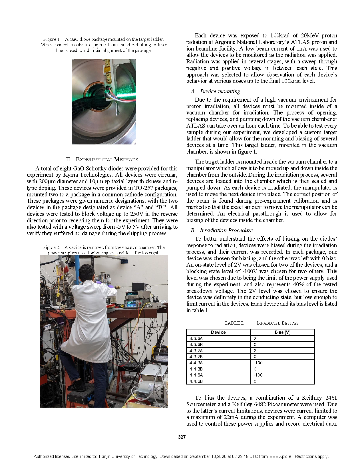
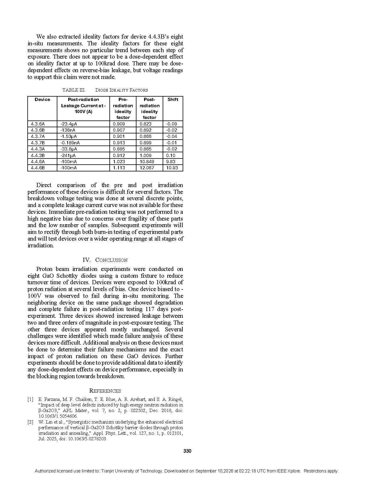
One device failed directly during irradiation under -100 V bias, while another co-packaged device subsequently experienced severe degradation; after 117 days post-irradiation testing revealed that three additional devices showed an increase in reverse leakage current at -100 V by approximately 2 to 3 orders of magnitude.
Conclusion
Proton beam irradiation experiments were conducted on eight GaO Schottky diodes using a custom fixture to reduce turnover time of devices. Devices were exposed to 100krad of proton radiation at several levels of bias. One device biased to - 100V was observed to fail during in-situ monitoring. The neighboring device on the same package showed degradation and complete failure in post-radiation testing 117 days post-experiment. Three devices showed increased leakage between two and three orders of magnitude in post-exposure testing. The other three devices appeared mostly unchanged. Several challenges were identified which made failure analysis of these devices more difficult. Additional analysis on these devices must be done to determine their failure mechanisms and the exact impact of proton radiation on these GaO devices. Further experiments should be done to provide additional data to identify any dose-dependent effects on device performance, especially in the blocking region towards breakdown.
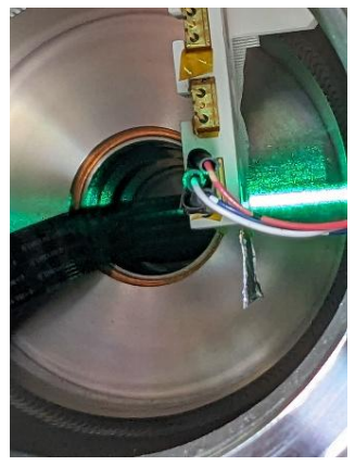
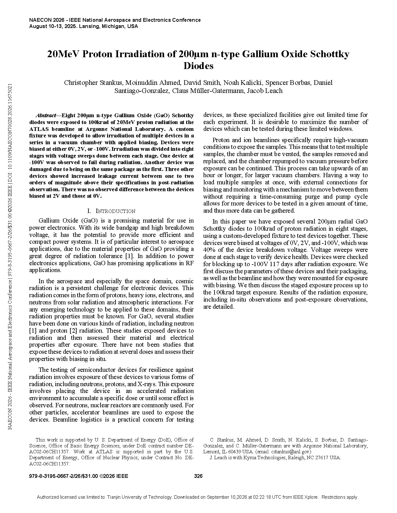
Figure 1. A GaO diode package mounted on the target ladder. Wires connect to outside equipment via a bulkhead fitting. A laser line is used to aid initial alignment of the package.
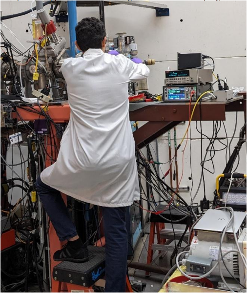
Figure 2. A device is removed from the vacuum chamber. The power supplies used for biasing are visible at the top right.
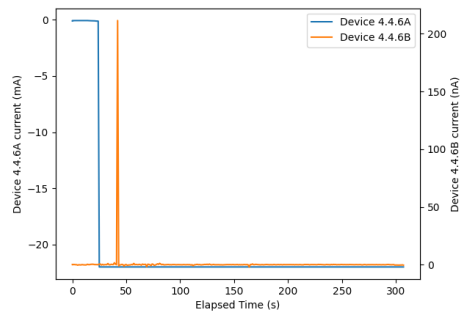
Figure 3. In-situ current measurement of devices 4.4.6A and 4.4.6B. 4.4.6A’s current falls sharply when the beam turns on, and shortly after a spike in current is seen in device 4.4.6B.
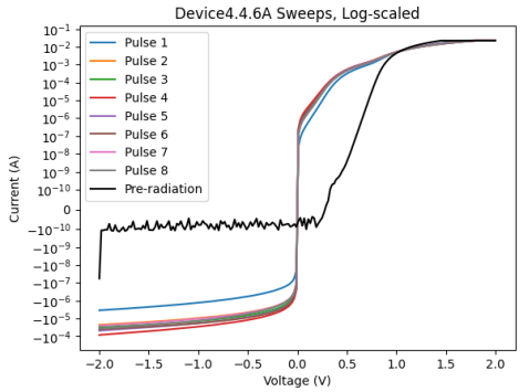
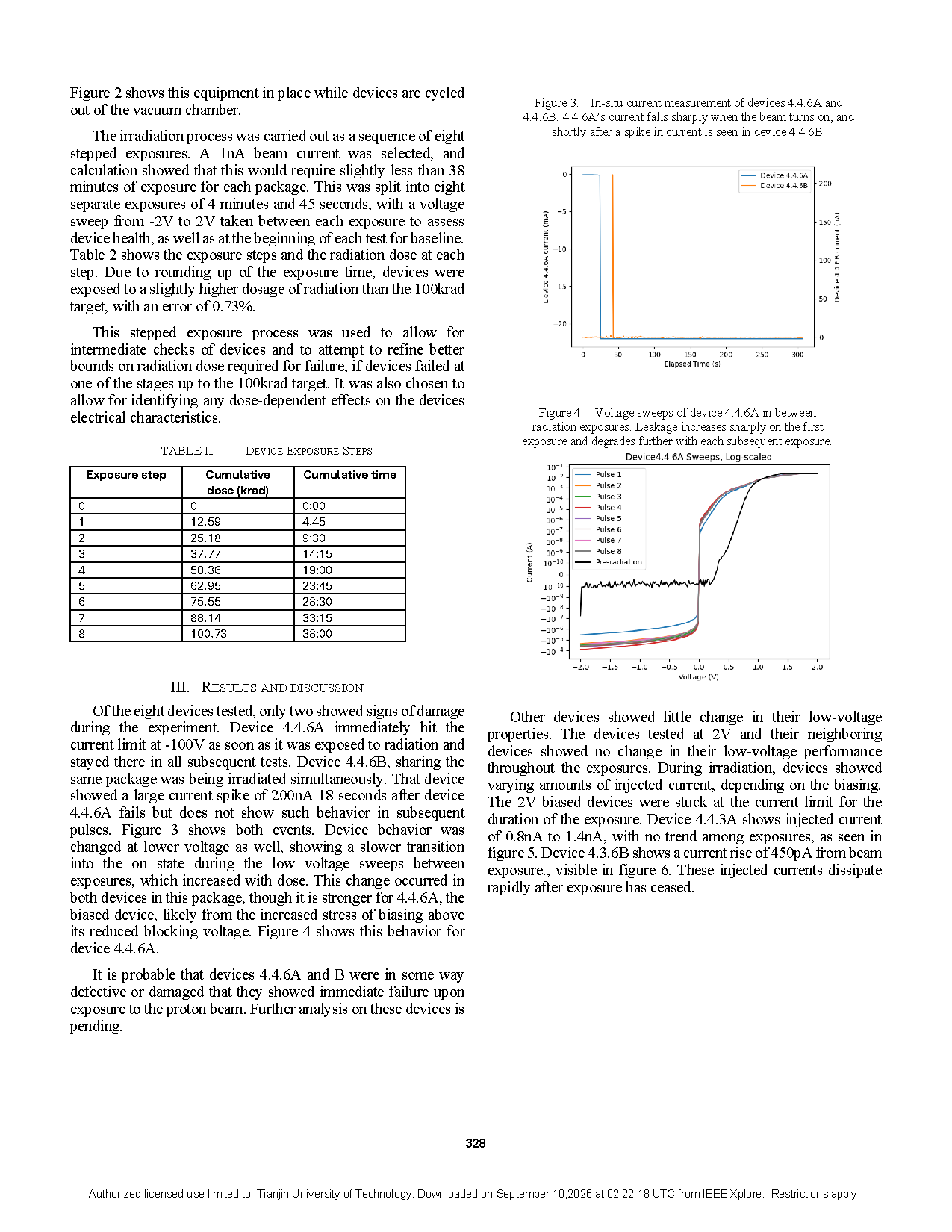
Figure 4. Voltage sweeps of device 4.4.6A in between radiation exposures. Leakage increases sharply on the first exposure and degrades further with each subsequent exposure.
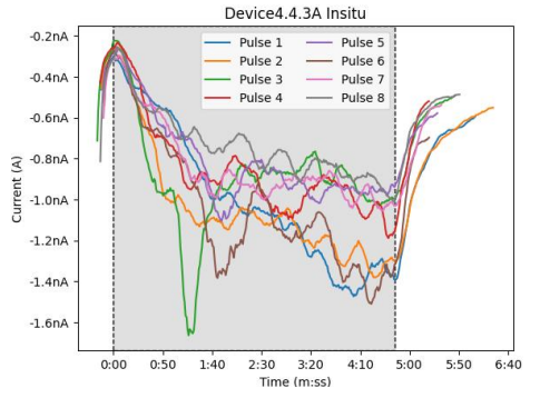
Figure 5. In-situ currents of device 4.4.3A, 15 second moving average. Current is a result of protons injected into the device, following the negative applied bias.
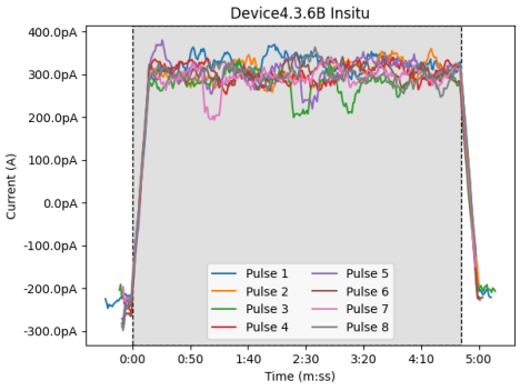
Figure 6. In-situ current of device 4.3.6B, biased at 0 V. 15 second moving average. Shaded region indicates when proton beam was present.
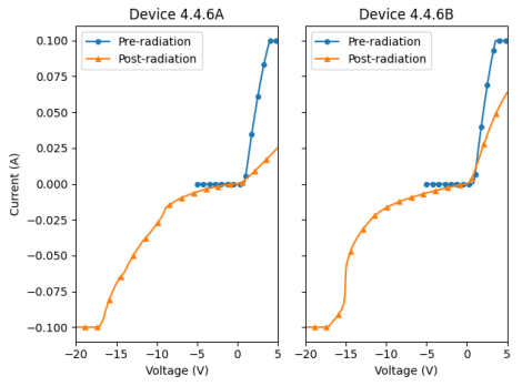
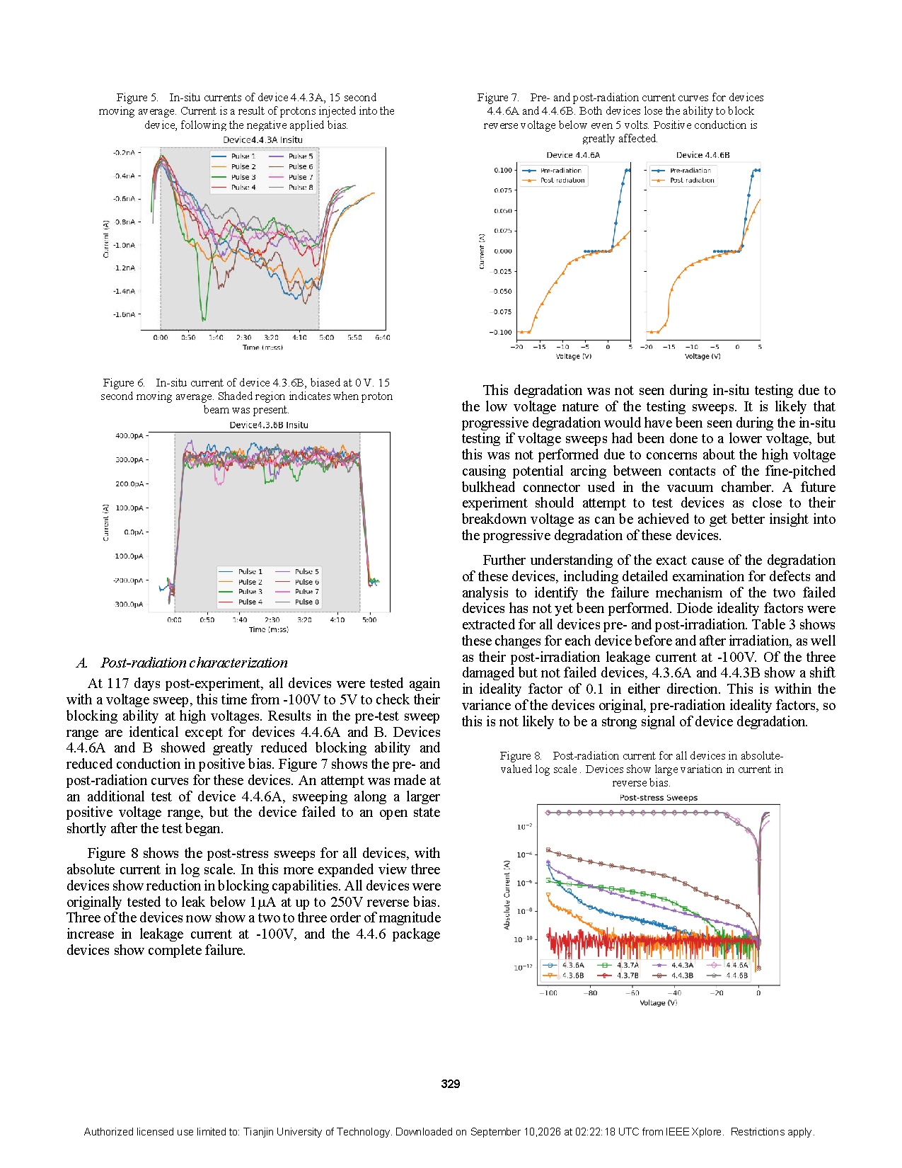
Figure 7. Pre- and post-radiation current curves for devices 4.4.6A and 4.4.6B. Both devices lose the ability to block reverse voltage below even 5 volts. Positive conduction is greatly affected.
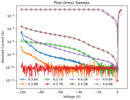
Figure 8. Post-radiation current for all devices in absolute-valued log scale. Devices show large variation in current in reverse bias.
DOI:
doi.org/10.1109/NAECON70028.2026.11675021
Instruction
Official Account

Cooperation
Top
