


Recently, Guangzhou Tanoxi Technology Co., Ltd. (hereinafter referred to as “the Company”) has secured an important advance in (010)-oriented thick-film Ga₂O₃ epitaxy.
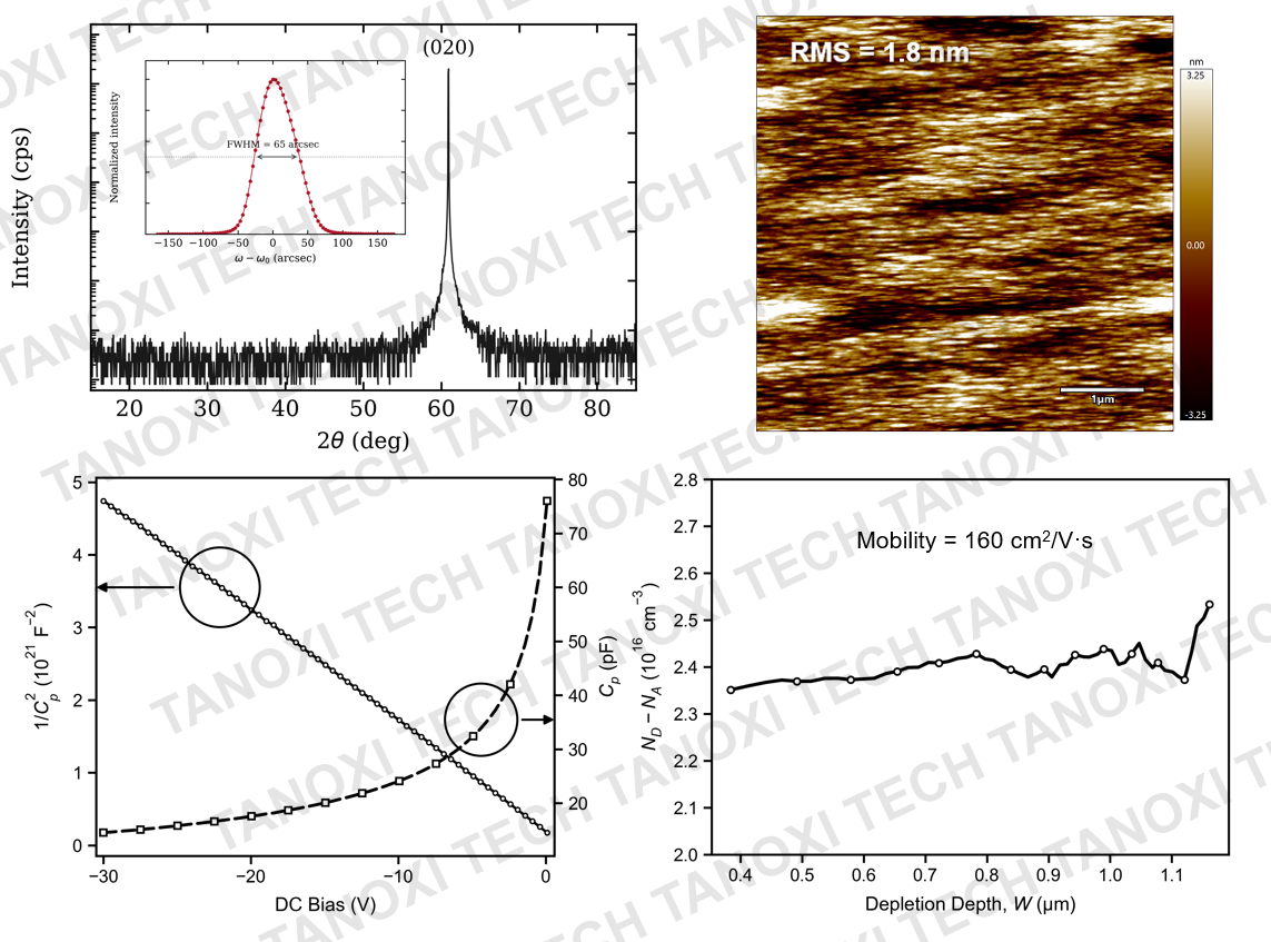
Adopting metal-organic chemical vapor deposition (MOCVD) technology, the Company has realized high-quality thick-film growth for (010) homoepitaxy. The epitaxial films possess a single-crystal structure, with room-temperature electron mobility of 160 cm²/V·s, doping concentration of 1.5 × 10¹⁶ cm⁻³, X-ray rocking-curve full width at half-maximum (FWHM) of 60 arcsec, and surface roughness below 2 nm.
The Company also offers customized services for homoepitaxial films with thickness ranging from 2 μm to 10 μm, where doping concentration can be precisely tuned within the range of 5 × 10¹⁶ cm⁻³ to 5 × 10¹⁸ cm⁻³.
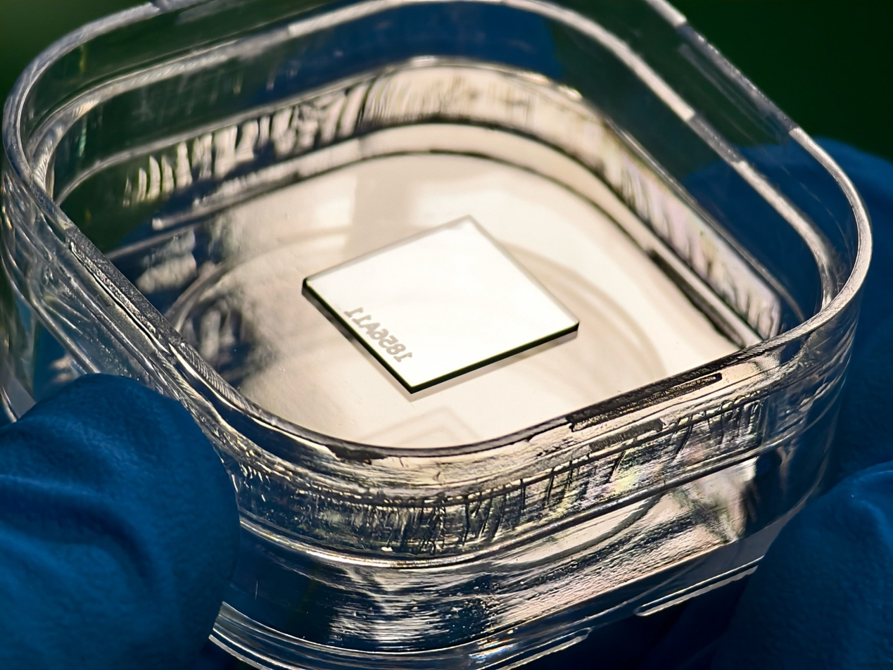
Figure 1 Photograph of Ga₂O₃ homoepitaxial wafer
Gallium oxide (Ga₂O₃) is a representative ultra-wide-bandgap semiconductor material for fourth-generation semiconductors. It features a bandgap of roughly 4.8-4.9 eV and a critical breakdown field strength as high as 8 MV/cm. Its Baliga’s figure-of-merit (BFOM) is far superior to that of silicon carbide (SiC) and gallium nitride (GaN).
Benefiting from its merits such as high withstand-voltage capability, low power loss, and the capability for low-cost preparation of large-size single-crystal substrates, Ga₂O₃ boasts broad application prospects in power electronics, radio-frequency (RF) devices, deep-ultraviolet (DUV) photodetection, smart sensing and other fields.
As China’s 15th Five-Year Plan Outline explicitly proposes to drive the industrial development of ultra-wide-bandgap semiconductors including Ga₂O₃, gallium oxide is accelerating its transformation from laboratory-scale research to engineering-oriented application.
β-Ga₂O₃ single crystals show prominent anisotropy. Different crystal planes each have their own strengths in terms of substrate dimension, epitaxy approaches and device performance, forming a mutually-complementary pattern.
The (100) plane has achieved rapid advances in large-size substrate development; 8- to 12-inch-grade substrates have been realized at present. It possesses great mass-production potential and serves as a key technical route for low-cost, large-volume manufacturing of Ga₂O₃.
Epitaxy on the (001) plane mainly adopts the halide vapor-phase epitaxy (HVPE) technique. It delivers fast growth rates and high epitaxy efficiency. Device performance of relevant structures has been verified by multiple parties, laying a sound foundation for power-device and high-voltage-scenario applications.
The (010) plane is widely recognized as one of the crystal orientations with the greatest potential for high electron mobility. Its theoretical upper limit of electron mobility approaches 200 cm²/V·s, rendering it a vital technical path for Ga₂O₃ devices featuring high on-state conduction and low power loss.
In the past, core technologies for high-quality thick-film epitaxy on the (010) plane were predominantly held by U.S. institutions. Domestic capabilities for high-quality thick-film epitaxy in this domain still called for key breakthroughs.
Leveraging its self-developed MOCVD thick-film epitaxy technology, the Company has accomplished a key breakthrough in (010) homoepitaxy. Synergistic control over film thickness, doping level, defects and surface flatness has been realized, enabling the capability for high-quality (010) thick-film epitaxy.
Key performance indicators are listed below:
Electron mobility: 160 cm²/V·s, an internationally-advanced performance level approaching the theoretical mobility potential of ~200 cm²/V·s for the (010) crystal plane.
Doping concentration: 1.5 × 10¹⁶ cm⁻³ (measured via the C-V method). Carrier concentration is precisely regulated to satisfy requirements for low-doped drift layers used in high-voltage power devices.
Crystal quality: Single-crystal epitaxy with outstanding lattice integrity.
X-ray rocking-curve FWHM: 60 arcsec, representing internationally-leading crystal-quality performance.
Surface roughness: Below 2 nm. AFM measurements confirm atomically-smooth epitaxial surfaces, offering an ideal interface for subsequent device manufacturing processes.
The Company provides customized (010) homoepitaxial film services to meet different customer requirements:
Epitaxial thickness: Flexibly tunable from 2 to 10 μm;
Doping concentration: Precisely controllable from 1 × 10¹⁶ to 1 × 10¹⁸ cm⁻³;
Epitaxy type: Homoepitaxy with single-crystal quality;
Substrate size: Supports 2- to 4-inch substrates and larger sizes;
Application areas: High-voltage power devices, RF devices, deep-ultraviolet (DUV) photodetectors, and related applications.
The three major crystal planes of (100), (001) and (010) do not serve as mutually-replacing technical paths. Instead, they deliver complementary strengths for distinct application scenarios. The Company will sustain close cooperation with industrial partners working on the large-size (100) technical route, the (001) HVPE route and other related approaches. Together, all parties will drive collaborative innovation across the full Ga₂O₃ industrial chain covering substrates, epitaxy and devices.
The Company aims to supply customers with integrated “epitaxy-to-device” one-stop solutions, and facilitate the industrialization of Ga₂O₃ power devices out of laboratory R&D environments.
Company Profile
Guangzhou Tanoxi Technology Co., Ltd. was founded in May 2022. It is a technology-focused enterprise specializing in the R&D, production and sales of gallium-oxide epitaxial materials and devices.
Centered on its self-developed Ga₂O₃ epitaxy technology, the Company has built an industrial-grade production line for Ga₂O₃ thin films with fully independent intellectual property rights. Through precise modulation of key epitaxy-process parameters, the Company’s products have reached internationally-advanced benchmarks on a full set of performance indicators.
The Company devotes itself to R&D and manufacturing of high-quality Ga₂O₃ epitaxial materials, so as to satisfy the market demand for power-electronic devices in sectors such as new-energy vehicles, State Grid of China, rail transit and 5G communications. It strives to deliver domestically self-controllable core-material guarantee and technical-support solutions for the country.
Website:www.tanoxitech.com
Contact
Email: contact@tnxtech.cn
Tel: +86 191 2051 6329
Instruction
Official Account

Cooperation
Top
