



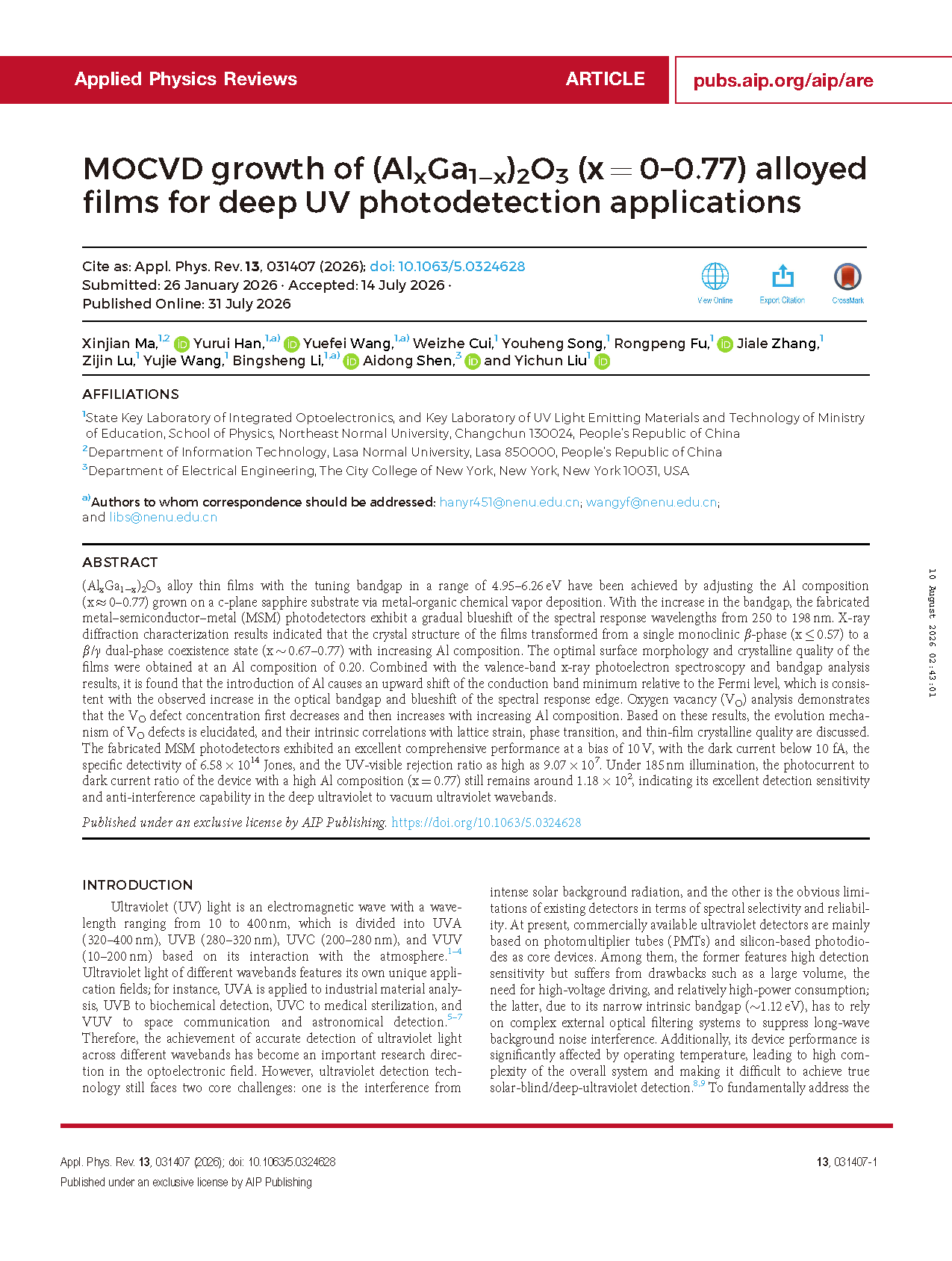
Researchers from the State Key Laboratory of Integrated Optoelectronics, Key Laboratory of UV Light Emitting Materials and Technology of Ministry of Education, School of Physics, Northeast Normal University; Department of Information Technology, Lasa Normal University; Department of Electrical Engineering, The City College of New York have published a dissertation titled " MOCVD growth of (AlₓGa₁₋ₓ)₂O₃ (x=0-0.77) alloyed films for deep UV photodetection applications" in Applied Physics Review.
Background
Ultraviolet (UV) light is an electromagnetic wave with a wavelength ranging from 10 to 400 nm, which is divided into UVA (320–400 nm), UVB (280–320 nm), UVC (200–280 nm), and VUV (10–200 nm) based on its interaction with the atmosphere. Different UV wavebands have unique application scenarios, such as industrial material analysis, biochemical detection, medical sterilization, space communication and astronomical detection. Accurate multi-band UV detection has become a key research topic in optoelectronics. Commercially available UV detectors mainly include photomultiplier tubes (PMTs) and silicon-based photodiodes. PMTs suffer from large volume, high-voltage driving and high power consumption. Silicon-based devices have a narrow bandgap of 1.12 eV and require complex optical filters to suppress background noise, and their performance is sensitive to operating temperature, which limits true solar-blind deep-UV detection. Wide-bandgap semiconductors provide promising solutions. Among them, β‑Ga₂O₃ is a hot candidate for solar-blind UV detection owing to its ~4.9 eV bandgap, large UV absorption coefficient and high breakdown field strength. Alloying is an effective band-gap-engineering approach. The bandgap of the ternary (AlₓGa₁₋ₓ)₂O₃ alloy covers UVC to VUV spectral range. Nevertheless, high-Al-content films suffer from phase transformation and phase separation, resulting in degraded crystalline quality. Most reported researches focus on low-to-medium Al compositions. Systematic understanding of phase stability, oxygen vacancy (VO) defect evolution and their correlation with device performance under high-Al conditions is still insufficient, which hinders the development of high-performance VUV photodetectors.
Abstract
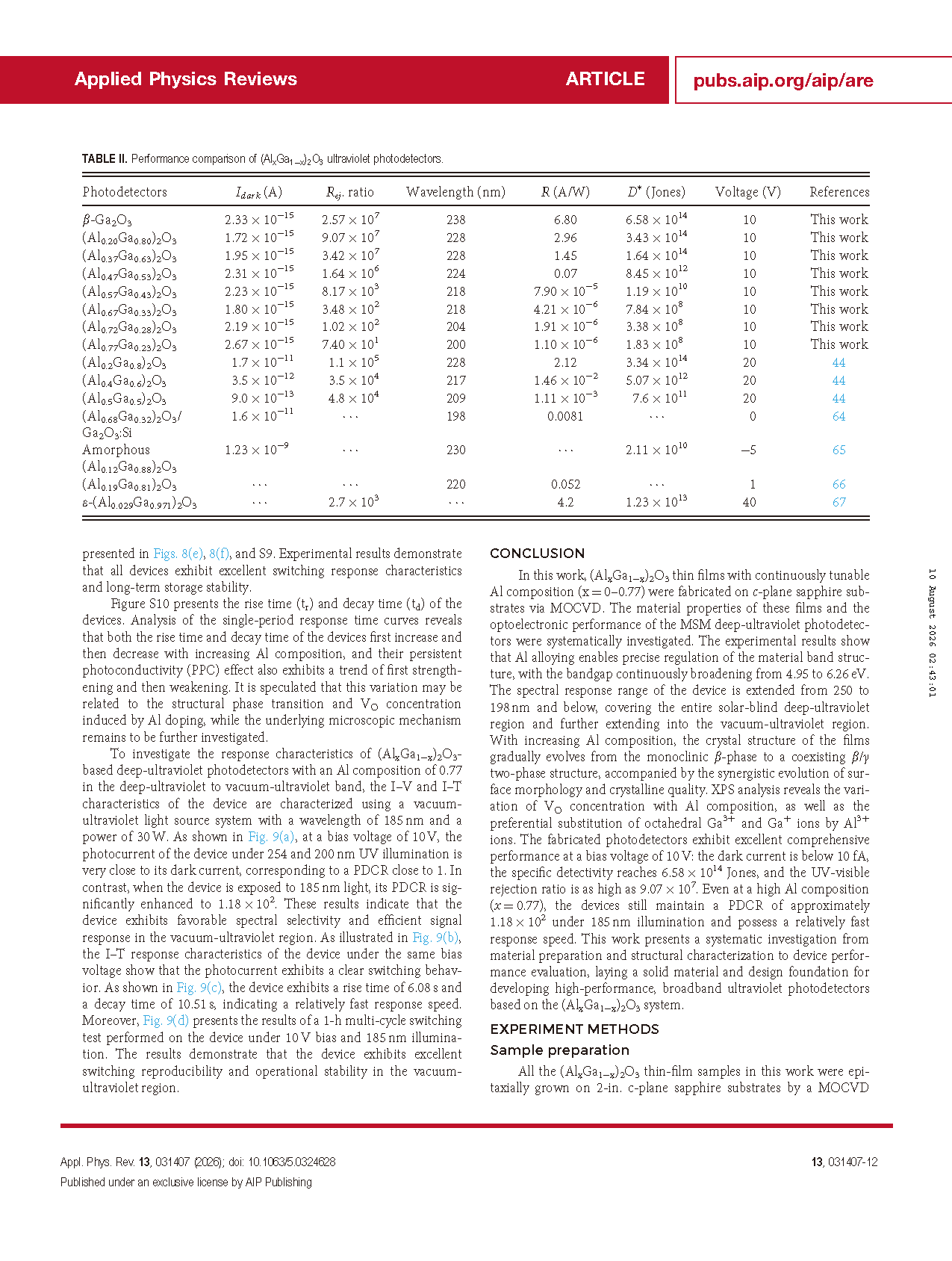
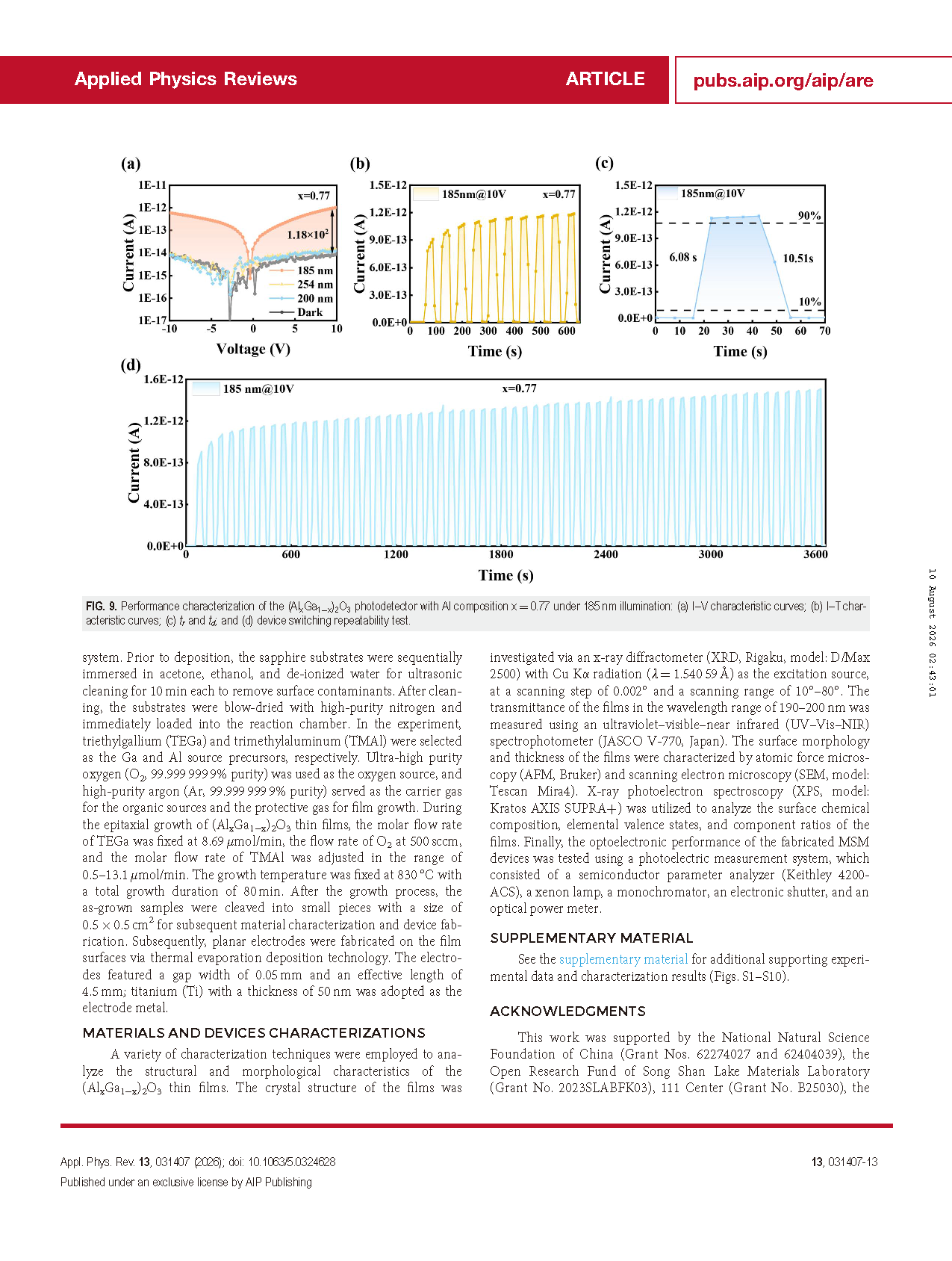
(AlₓGa₁₋ₓ)₂O₃ alloy thin films with the tuning bandgap in a range of 4.95–6.26 eV have been achieved by adjusting the Al composition (x ≈0-0.77) grown on a c-plane sapphire substrate via metal-organic chemical vapor deposition. With the increase in the bandgap, the fabricated metal–semiconductor–metal (MSM) photodetectors exhibit a gradual blueshift of the spectral response wavelengths from 250 to 198 nm. X-ray diffraction characterization results indicated that the crystal structure of the films transformed from a single monoclinic β-phase (x ≤0.57) to a β/γ dual-phase coexistence state (x=0.67-0.77) with increasing Al composition. The optimal surface morphology and crystalline quality of the films were obtained at an Al composition of 0.20. Combined with the valence-band X-ray photoelectron spectroscopy and bandgap analysis results, it is found that the introduction of Al causes an upward shift of the conduction band minimum relative to the Fermi level, which is consistent with the observed increase in the optical bandgap and blueshift of the spectral response edge. Oxygen vacancy (VO) analysis demonstrates that the VO defect concentration first decreases and then increases with increasing Al composition. Based on these results, the evolution mechanism of VO defects is elucidated, and their intrinsic correlations with lattice strain, phase transition, and thin-film crystalline quality are discussed. The fabricated MSM photodetectors exhibited an excellent comprehensive performance at a bias of 10 V, with the dark current below 10 fA, the specific detectivity of 6.58 ×10¹⁴ Jones, and the UV-visible rejection ratio as high as 9.07 ×10⁷. Under 185 nm illumination, the photocurrent to dark current ratio of the device with a high Al composition (x=0.77) still remains around 1.18 ×10², indicating its excellent detection sensitivity and anti-interference capability in the deep ultraviolet to vacuum ultraviolet wavebands.
Highlights
The team successfully grew high-quality (AlₓGa₁₋ₓ)₂O₃ alloy thin films with an Al composition as high as 0.77 on c-plane sapphire substrates via MOCVD, achieving a continuously tunable bandgap from 4.95 eV to 6.26 eV.
Clarification of phase-transition boundary and lattice-defect evolution. The team identified the critical Al composition for phase transition from single monoclinic β phase to β/γ dual-phase coexistence. They revealed that oxygen vacancy VO concentration decreases first and then increases with increasing Al content, and discussed intrinsic correlations among lattice strain, phase transition, crystalline quality and oxygen-vacancy defects.
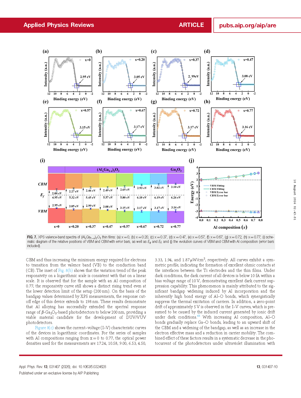
Through XPS analysis, the team revealed that Al alloying causes an upward shift of the conduction band minimum (CBM), thereby widening the bandgap.
High-performance MSM photodetectors with spectral response extended to vacuum-ultraviolet region. Metal-semiconductor-metal (MSM) photodetectors were fabricated with cut-off wavelength blue-shifted to 198 nm. Devices achieve ultra-low dark current, ultra-high specific detectivity and large UV-visible rejection ratio. High-Al-content device maintains considerable photocurrent-to-dark-current ratio under 185 nm VUV illumination, validating its VUV detection potential.
Conclusion
In this work, (AlₓGa₁₋ₓ)₂O₃ thin films with continuously tunable Al composition (x=0-0.77) were fabricated on c-plane sapphire substrates via MOCVD. The material properties of these films and the optoelectronic performance of the MSM deep-ultraviolet photodetectors were systematically investigated. The experimental results show that Al alloying enables precise regulation of the material band structure, with the bandgap continuously broadening from 4.95 to 6.26 eV.The spectral response range of the device is extended from 250 to 198 nm and below, covering the entire solar-blind deep-ultraviolet region and further extending into the vacuum-ultraviolet region. With increasing Al composition, the crystal structure of the films gradually evolves from the monoclinic β-phase to a coexisting β/γ two-phase structure, accompanied by the synergistic evolution of surface morphology and crystalline quality. XPS analysis reveals the variation of VO concentration with Al composition, as well as the preferential substitution of octahedral Ga³⁺ and Ga⁺ ions by Al³⁺ ions.The fabricated photodetectors exhibit excellent comprehensive performance at a bias voltage of 10 V: the dark current is below 10 fA, the specific detectivity reaches 6.58×10¹⁴ Jones, and the UV-visible rejection ratio is as high as 9.07×10⁷. Even at a high Al composition (x=0.77), the devices still maintain a PDCR of approximately 1.18×10² under 185 nm illumination and possess a relatively fast response speed. This work presents a systematic investigation from material preparation and structural characterization to device performance evaluation, laying a solid material and design foundation for developing high-performance, broadband ultraviolet photodetectors based on the (AlₓGa₁₋ₓ)₂O₃ system.
Project Support
This work was supported by the National Natural Science Foundation of China (Grant Nos. 62274027 and 62404039), the Open Research Fund of Song Shan Lake Materials Laboratory (Grant No. 2023SLABFK03), 111 Center (Grant No. B25030), Jilin Province (Grant No. 20220502002 GH), and the Scientific Research Project of Education Department of Jilin Province (Grant No. JJKH20250304BS).
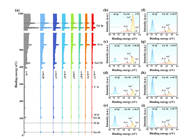
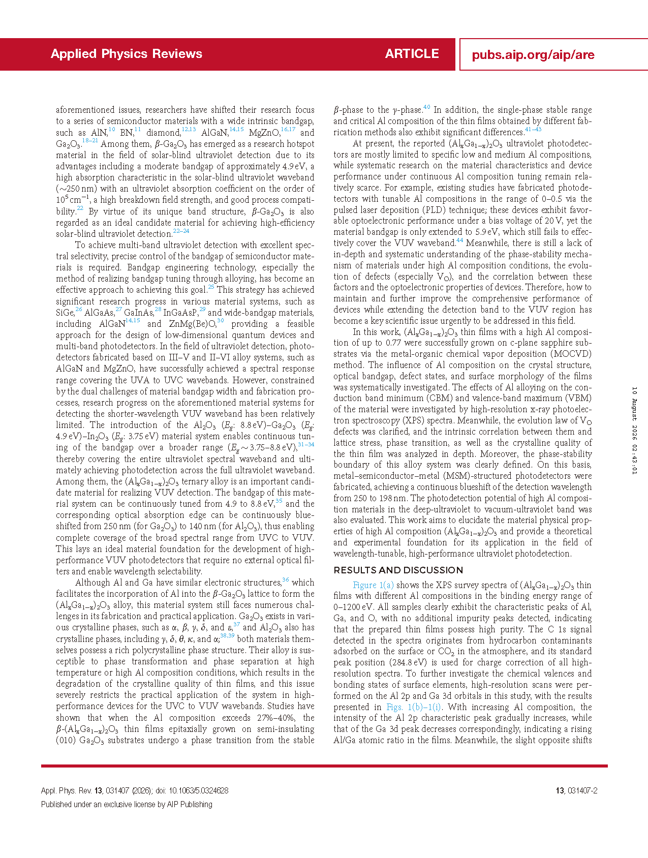
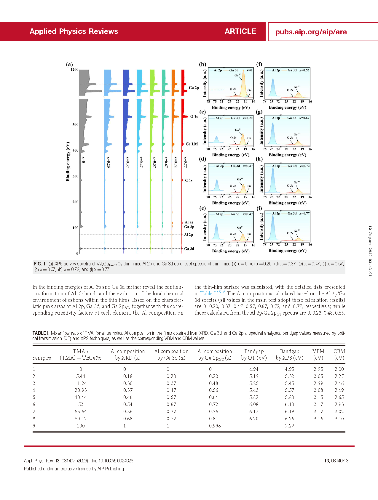
Fig. 1. (a) XPS survey spectra of(AlₓGa₁₋ₓ)₂O₃ thin films. Al 2p and Ga 3d core-level spectra of thin films: (b) x=0, (c) x=0.20, (d) x=0.37, (e) x=0.47, (f) x=0.57, (g) x=0.67, (h) x=0.72, and (i) x=0.77.
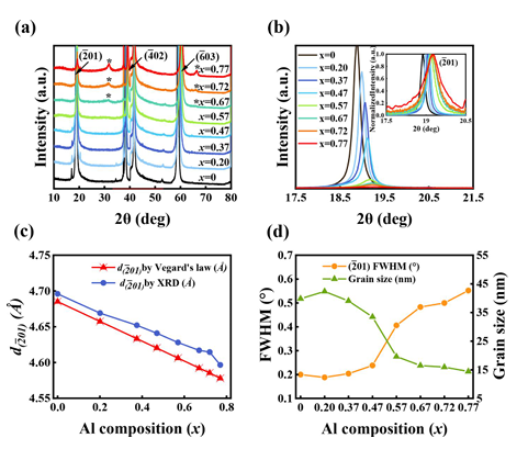
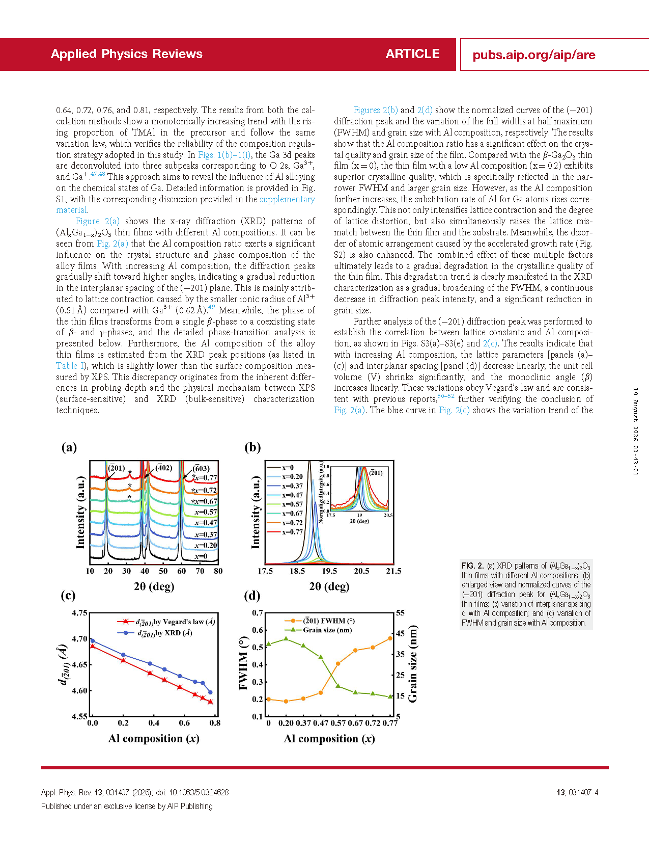
Fig. 2. (a) XRD patterns of (AlₓGa₁₋ₓ)₂O₃ thin films with different Al compositions; (b) enlarged view and normalized curves of the (−201) diffraction peak for (AlₓGa₁₋ₓ)₂O₃ thin films; (c) variation of interplanar spacing d with Al composition; and (d) variation of FWHM and grain size with Al composition.
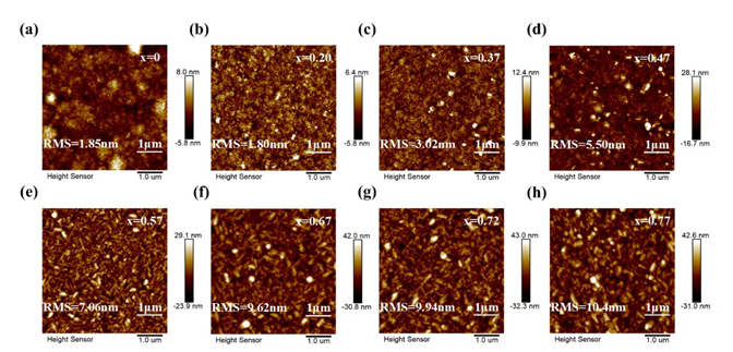
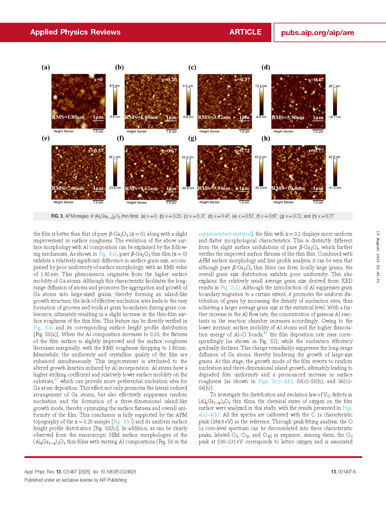
Fig. 3. AFM images of (AlₓGa₁₋ₓ)₂O₃ thin films: (a) x=0, (b) x=0.20, (c) x=0.37, (d) x=0.47, (e) x=0.57, (f) x=0.67, (g) x=0.72 and (h) x=0.77.
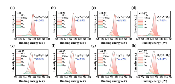
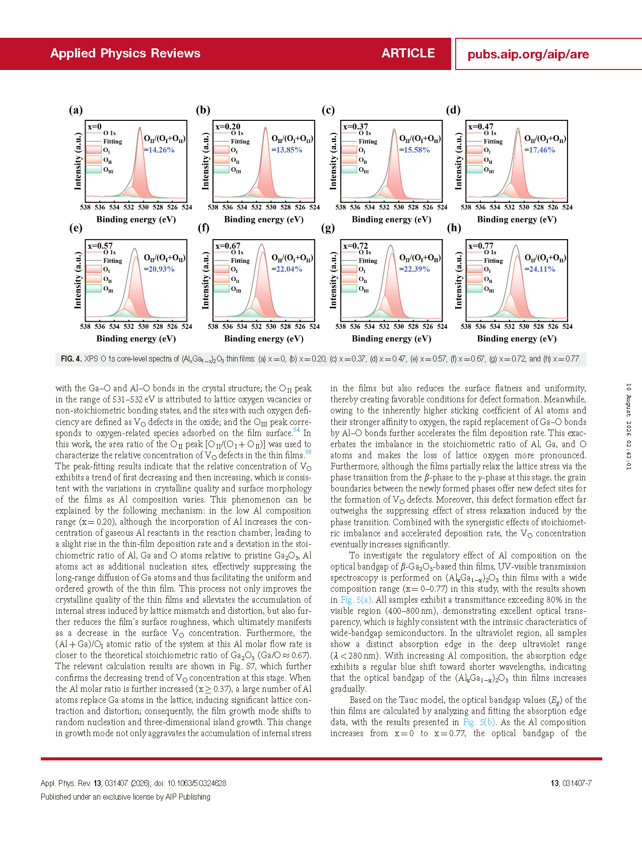
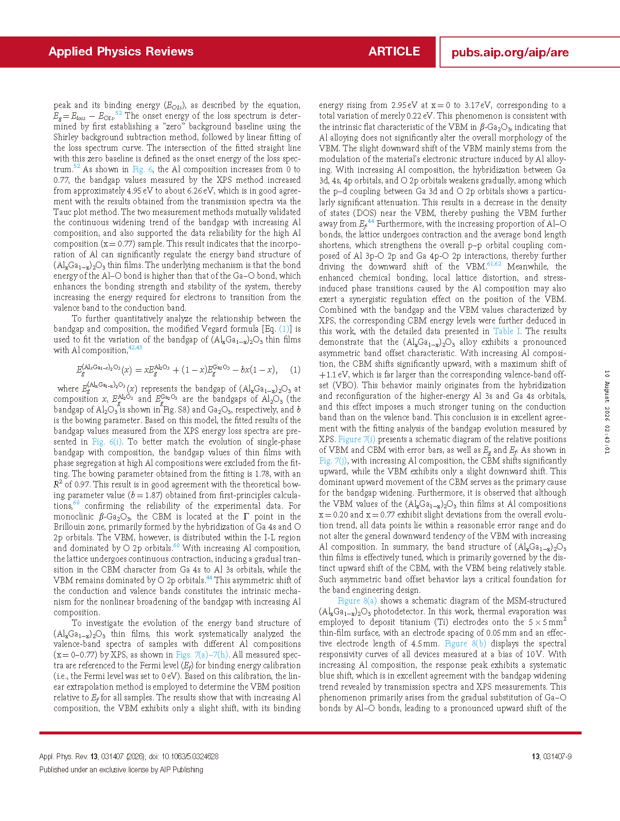
Fig. 4. XPS O 1s core‑level spectra of (Alₓ Ga₁₋ₓ)₂ O₃ thin films: (a) x=0, (b) x=0.20, (c) x=0.37, (d) x=0.47, (e) x=0.57, (f) x=0.67, (g) x=0.72 and (h) x=0.77.
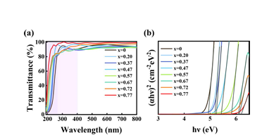
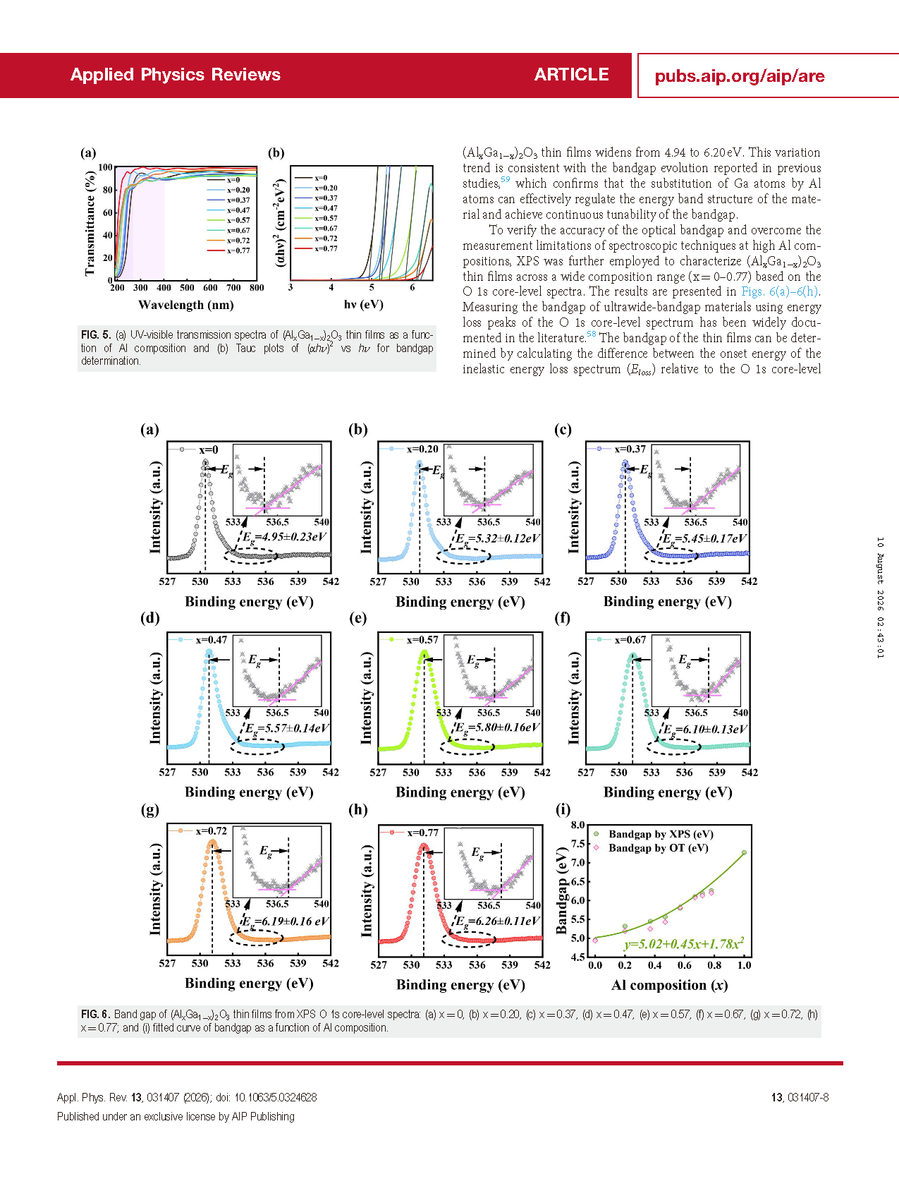
Fig. 5. (a) UV‑visible transmission spectra of (AlₓGa₁₋ₓ)₂O₃ thin films as a function of Al composition and (b) Tauc plots of (αhν)² vs hν for bandgap determination.
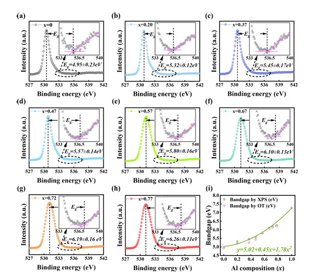
Fig. 6. Band gap of (AlₓGa₁₋ₓ)₂O₃thin films from XPS O 1s core‑level spectra: (a) x=0, (b) x=0.20, (c) x=0.37, (d) x=0.47, (e) x=0.57, (f) x=0.67, (g) x=0.72, (h) x=0.77; and (i) fitted curve of bandgap as a function of Al composition.
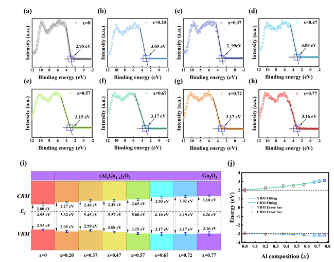
Fig. 7. XPS valence‑band spectra of(AlₓGa₁₋ₓ)₂O₃thin films: (a) x=0, (b) x=0.20, (c) x=0.37, (d) x=0.47, (e) x=0.57, (f) x=0.67, (g) x=0.72, (h) x=0.77; (i) schematic diagram of the relative positions of VBM and CBM with error bars, as well as Eg and EF; and (j) the evolution curves of VBM and CBM with Al composition (error bars included).
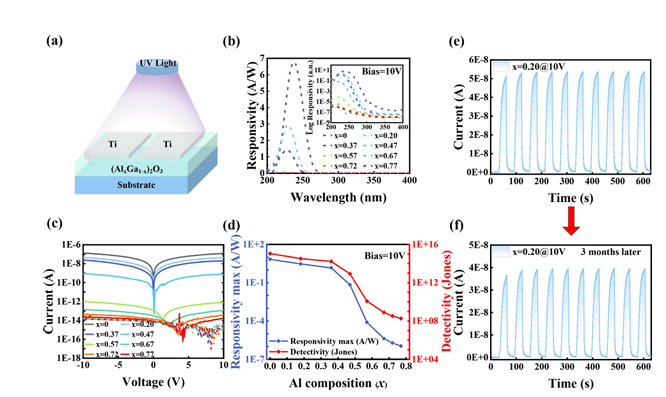
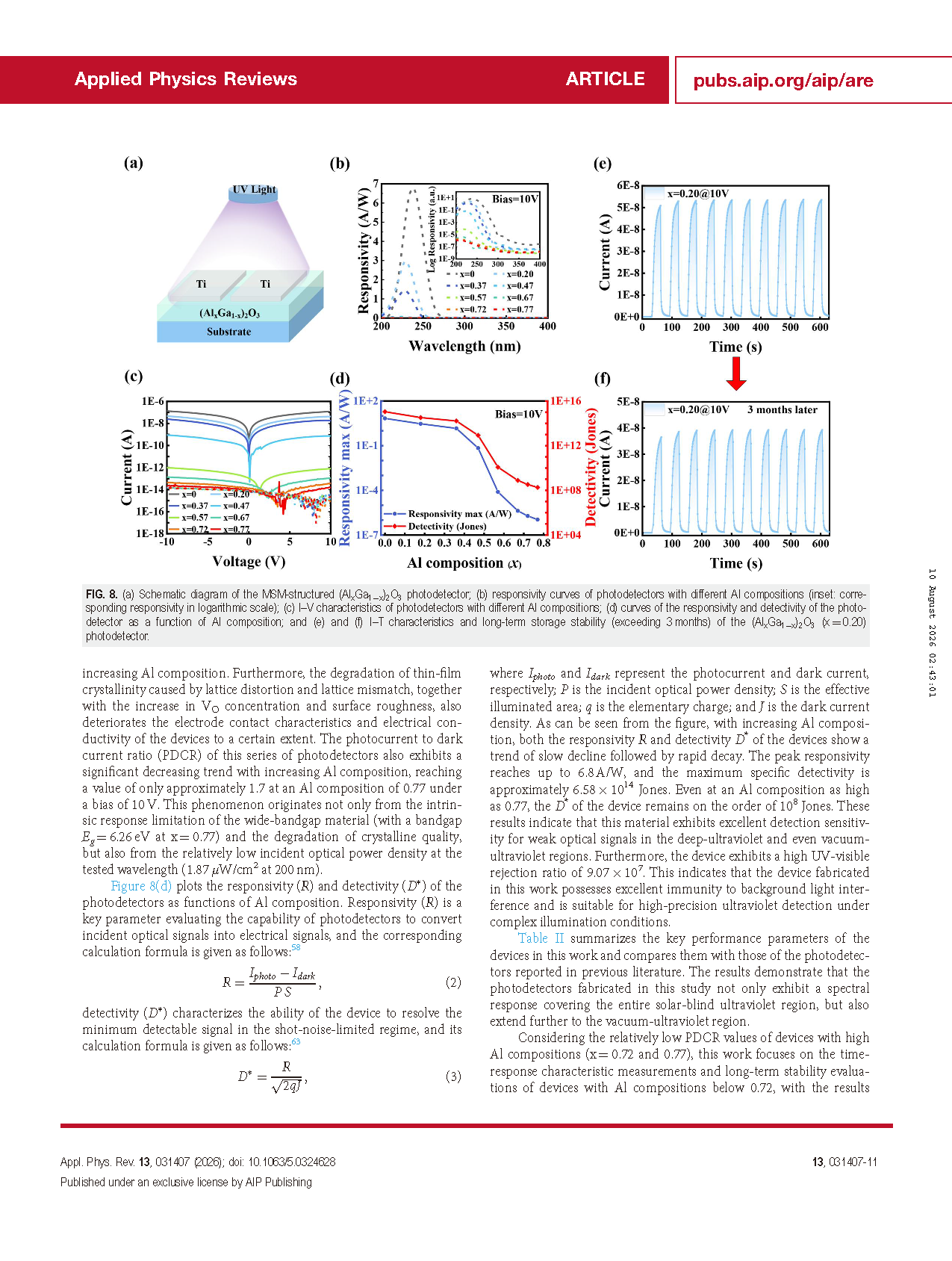
Fig. 8. (a) Schematic diagram of the MSM-structured(AlₓGa₁₋ₓ)₂O₃ photodetector; (b) responsivity curves of photodetectors with different Al compositions (inset: corresponding responsivity in logarithmic scale); (c) I-V characteristics of photodetectors with different Al compositions; (d) curves of the responsivity and detectivity of the photodetector as a function of Al composition; and (e) and (f) I-T characteristics and long-term storage stability (exceeding 3 months) of the(AlₓGa₁₋ₓ)₂O₃ (x=0.20) photodetector.
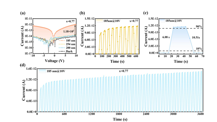
Fig. 9. Performance characterization of the(AlₓGa₁₋ₓ)₂O₃ photodetector with Al composition x=0.77 under 185 nm illumination: (a) I‑V characteristic curves; (b) I‑T characteristic curves; (c) tᵣ and td; and (d) device switching repeatability test.
DOI:
10.1063/5.0324628


Instruction
Official Account

Cooperation
Top
