


2026: A Pivotal Year for ε-Ga₂O₃
Recently, an industry research report focusing on cutting‑edge technologies of fourth‑generation compound semiconductors points out that gallium oxide (Ga₂O₃), a fourth‑generation compound semiconductor material featuring unique properties including piezoelectricity and an ultra‑wide bandgap, is transitioning from laboratory R&D toward industrial application. Over the next five years, it will move from R&D verification to large‑scale commercialization, with competition shifting its focus toward full‑value‑chain collaboration and cost control.

From the Laboratory to Industrial Deployment:
The Strategic Window for Ga₂O₃ Is Now Fully Open
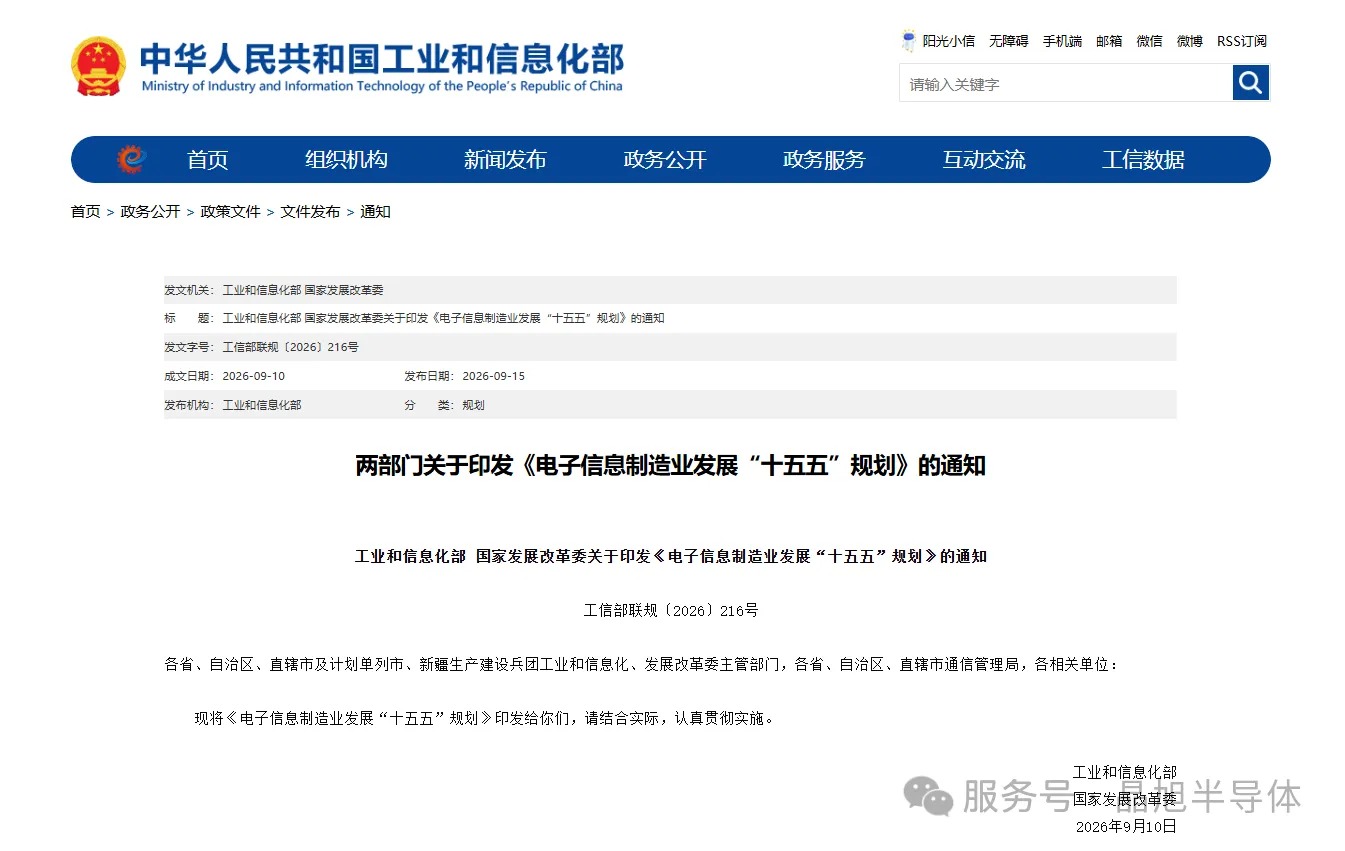
China’s “15th Five-Year Plan for the Development of the Electronic Information Manufacturing Industry” has, for the first time, incorporated the industrialization of gallium oxide (Ga₂O₃) into the national strategic agenda, explicitly identifying Ga₂O₃ as a key direction for ultra-wide-bandgap semiconductors.
The Plan clearly states: “Promote the upgrading and development of the wide-bandgap semiconductor industry, and advance the industrialization of ultra-wide-bandgap semiconductors such as gallium oxide and diamond.”
Sunwise Semiconductor:
A Full-Chain Breakthrough from Core Materials to Key Equipment
Amid the global race for gallium oxide (Ga₂O₃) commercialization, Sunwise Semiconductor has drawn on more than two decades of accumulated technological expertise to build a complete technology chain covering materials, processes and equipment.
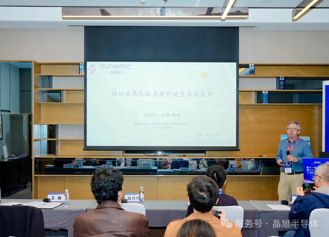
For many years, AlN-based systems have dominated the core piezoelectric materials used in global bulk acoustic wave (BAW) filters. Sunwise Semiconductor has taken a different approach from the conventional technology route. After more than two decades of dedicated R&D, the company successfully overcame the challenges associated with the industrialization and application of silicon-based heteroepitaxial ε-Ga₂O₃ piezoelectric thin films in 2023.
The company has achieved original innovations across materials, processes, equipment, and theoretical research. Its key performance metrics are reported to be more than 20% higher than those of comparable products overseas. According to the company, Sunwise Semiconductor is currently the only company worldwide with the capability to independently mass-produce and deliver Ga₂O₃-based piezoelectric materials for BAW filters.
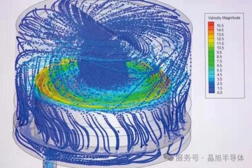
On the equipment front, the company has independently developed the world’s first dedicated MOCVD system for ε‑Ga₂O₃ epitaxy, conquering core technologies including chamber flow‑field and thermal‑field optimization and high‑temperature anti‑oxidation heating.
The system achieves top‑tier industry‑leading core parameters: FWHM < 0.6°, film‑thickness uniformity < 2%, stress < 500 MPa. The material features minimal internal defects — C‑axis orientation > 98%, porosity < 0.1%, dislocation density < 10⁶ cm⁻² — outperforming other comparable piezoelectric materials and fully satisfying the requirements for practical mass‑production deployment.
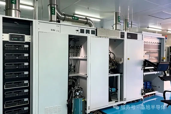
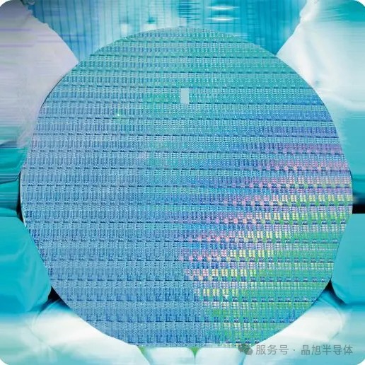
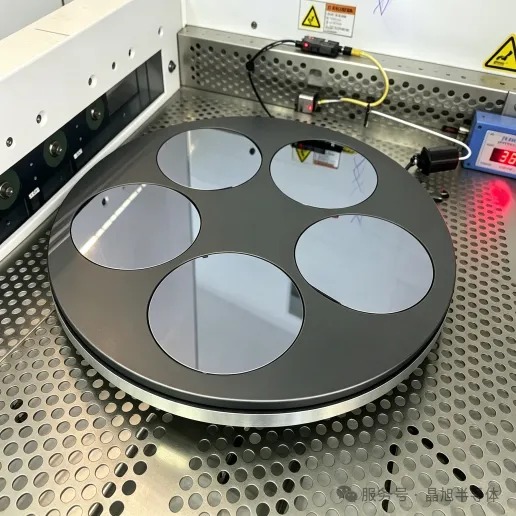
On the product front, drawing on its self-developed thin-film technology, Sunwise Semiconductor has realized mass production of high-yield ε-Ga₂O₃-based POI wafers with production yield exceeding 97%. These wafers support filtering requirements for ultra-high frequencies of 2 GHz-10 GHz and ultra-wide bandwidth of 100 MHz-1.5 GHz, with in-band insertion loss below 2 dB. Compared with conventional BAW filters, they double the power-handling capacity and deliver prominent advantages for high-frequency communications and wide-band IoT scenarios.
N Notably, Sunwise Semiconductor adopts a silicon-based heteroepitaxial process that cuts costs by 50 % compared with conventional doped piezoelectric material solutions. By the end of 2026, Sunwise will put an 8-inch mass-production line for gallium-oxide piezoelectric materials into operation to further drive down manufacturing costs and accelerate large-scale popularization of the technology. This cost advantage serves as a prime practical illustration of the industry-wide shift “from material-performance-oriented competition toward full-value-chain collaboration and cost control”.This cost advantage provides a concrete example of the industry’s broader shift in focus from material performance alone toward end-to-end value-chain collaboration and cost control.
Accelerating Commercialization:
The World’s First Production Line Is Set to Enter Full-Scale Operation
Beyond its technological breakthroughs, Sunwise Semiconductor is also advancing its commercialization strategy at the forefront of the industry.
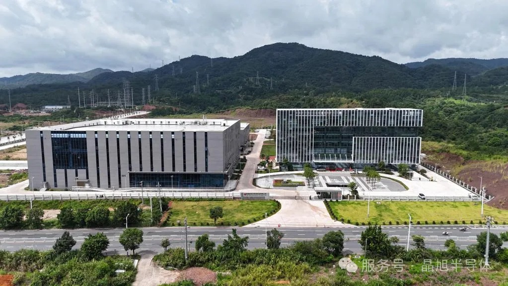
Located in the Shanghang Industrial Park in Longyan City, the company’s Ga₂O₃ piezoelectric thin-film new-material production project has a total investment of RMB 1.68 billion and covers an area of 136 mu (approximately 90.7 hectares).
Once completed, the project is expected not only to fill a gap in China’s domestic production of Ga₂O₃ piezoelectric thin-film materials, but also to provide critical material support for the development of 5G/6G communications, the Internet of Things (IoT), and advanced manufacturing worldwide.
See You at WESEMiBAY:
Witness the Strength of China’s Ga₂O₃ Solution
From October 14 to 16, 2026, WESEMiBAY 2026 — the Bay-Area Semiconductor Industry Ecosystem Expo — will grandly open at Shenzhen Convention and Exhibition Center (Futian). Sunwise Semiconductor will showcase its flagship products including Ga₂O₃-based piezoelectric materials for BAW filters, POI wafers and high-frequency filter chips at the expo, and engage with partners across the global semiconductor industrial chain to discuss the commercial future of fourth-generation semiconductors.
Why has 2026 become a pivotal year for ε-Ga₂O₃? It is not only because of the convergence of policy support, capital investment, and technological progress, but also because companies such as Sunwise Semiconductor are turning what was once merely “possible” into “feasible” through concrete action—from breaking overseas reliance through advances in core materials, to developing proprietary key equipment, and now to the upcoming full-scale operation of the world’s first production line of its kind.
Through these efforts, Sunwise Semiconductor is contributing a “China solution” to the global industrialization of fourth-generation semiconductors.
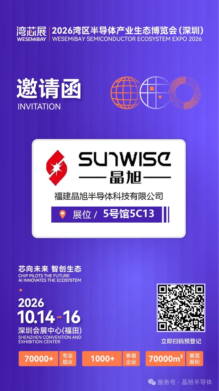
At the WESEMiBAY Semiconductor Ecosystem Expo in Shenzhen this October, Sunwise Semiconductor will be exhibiting at Hall 5, Booth 5C13. We look forward to welcoming you and witnessing together the arrival of the Ga₂O₃ era.
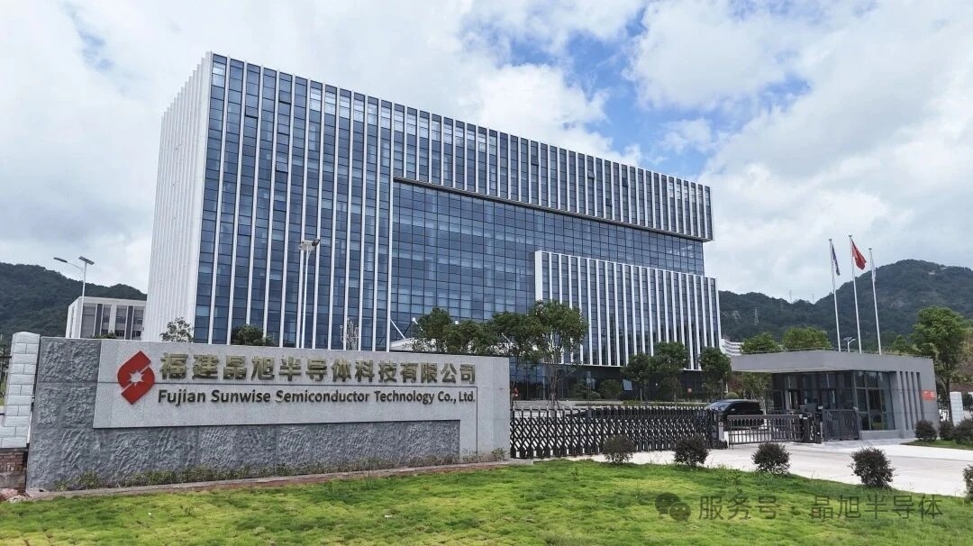
——— About Sunwise Semiconductor ———
Sunwise Semiconductor specializes in third-generation (GaN) and fourth-generation (ε-Ga₂O₃) ultra-wide-bandgap semiconductors as well as optoelectronic integration technologies. It is a high-tech enterprise with rare domestic capabilities for wafer-scale heterogeneous/hybrid integration platforms. Led by an academician-backed R&D team, the company independently masters world-leading technologies for single-crystal ε-Ga₂O₃ thin-film epitaxial growth and wafer-scale heterogeneous/hybrid integration, holding more than 100 core patents and a comprehensive portfolio of independently owned intellectual property rights.
Building on its leading heterogeneous/hybrid integration technologies, Sunwise has established a full-process workflow covering 'epitaxial growth — damage-free thin-film delamination — wafer-scale transfer and bonding — optoelectronic integrated packaging'. Its 8-inch-class wafer heterogeneous integration platform matches the process windows required for optical communication modulator chips. The company has already achieved mass-production delivery of GaN optoelectronic integrated packaging products. Its 6/8-inch ε-Ga₂O₃ epitaxy and substrate transfer product lines (ε-Ga₂O₃ POI) have entered the pilot-production / volume-ramp-up phase.
Looking ahead, Sunwise Semiconductor plans to extend its in-house heterogeneous integration processes to thin-film lithium niobate-on-insulator (LNOI) and silicon-on-insulator (SOI) platforms for optical modules supporting AI computing power and high-speed optical interconnects.
The company strives to collaborate with industry partners to break international bottlenecks imposed by monopolies over core materials and devices, advance the sound development of core materials for high-end chips and optical communication products, and grow into a world-leading enterprise for R&D, manufacturing and services of compound semiconductor materials.
Instruction
Official Account

Cooperation
Top
