


Researchers from the Institute of Microelectronics of Barcelona (IMB-CNM, CSIC), Institute of Solid State Physics, Univ. Latvia, and Groupe d'Etude de la Matière Condensée, Université Paris-Saclay GEMaC have published a dissertation titled "Impact of Si ion implantation on α- Ga₂O₃ and β-Ga₂O₃ lateral MESFET transistors" in Journal of Alloys and Compounds.
Background
Gallium oxide (Ga₂O₃), as an ultra-wide bandgap semiconductor, has attracted significant attention due to its high critical electric field (greater than 8 MV/cm) and relatively high electron mobility (~150-300 cm²/V·s), with a Baliga's figure of merit (BFOM) far exceeding those of silicon carbide (SiC) and gallium nitride (GaN). Ga₂O₃ presents multiple polymorphs, among which β-Ga₂O₃ is the thermodynamically stable phase and has become the primary focus of power device development, while α-Ga₂O₃ exhibits a wider bandgap (5.3-5.6 eV), enables high-quality heteroepitaxy on sapphire substrates, and supports bandgap engineering through α-(AlₓGa₁₋ₓ)₂O₃ alloys. However, α-Ga₂O₃ is metastable and undergoes a reconstructive phase transition to β-Ga₂O₃ at onset temperatures typically around 450-550 °C, posing a major obstacle for device fabrication.
Ion-implantation-based doping, widely used for selective channel and ohmic contact formation in β-Ga₂O₃ devices, generally requires post-implantation annealing temperatures of 900-1100 °C to repair lattice damage and electrically activate donors. This thermal budget requirement fundamentally conflicts with the phase stability window of α-Ga₂O₃. Although previous studies have adopted Al₂O₃ capping strategies to delay the phase transition, whether the thermal budget required for implantation-based dopant activation remains compatible with the metastability of α-Ga₂O₃ has not been systematically explored. This team presents the first direct comparison of Si-implanted α-Ga₂O₃ and β-Ga₂O₃ MESFETs fabricated using an equivalent process flow, evaluating the feasibility of implantation-based doping technology for α-Ga₂O₃ devices.
Abstract
In this work, the feasibility of Si ion‑implantation channel engineering in metastable α‑Ga₂O₃ is directly compared with the well‑established implantation process used in β‑Ga₂O₃ lateral MESFETs. Identical multi‑energy Si implantation schemes (10–200 keV) and thermal annealing conditions were applied to both polymorphs in order to evaluate the compatibility of implantation‑based doping with the thermal stability window of α‑Ga₂O₃. For β‑Ga₂O₃ Si implantation followed by high‑temperature annealing (900‑1100 °C) successfully enabled conductive channel and ohmic contact formation, leading to functional lateral MESFET operation with proper current modulation and saturation behaviour. In contrast, α‑Ga₂O₃ layers grown on m‑plane sapphire exhibited a strong limitation associated with their metastable nature. An ALD‑deposited Al₂O₃ capping layer delayed the α → β phase transition up to approximately 700 °C, as confirmed by X‑ray diffraction analysis. However, electrical measurements revealed no measurable channel conduction after annealing within this temperature range, suggesting that efficient electrical activation of the implanted Si donors was not achieved within the α‑Ga₂O₃ thermal stability window. At higher annealing temperatures, where dopant activation would normally be expected, the α‑phase underwent complete reconstructive transformation into β‑Ga₂O₃ accompanied by severe structural degradation and suppressed electrical transport. These results demonstrate that the thermal budget required for conventional implantation‑based donor activation exceeds the metastability window of α‑Ga₂O₃, even when thermal stabilization layers are employed. The study therefore identifies a fundamental technological limitation for ion‑implantation‑defined α‑Ga₂O₃ power devices and highlights the need for alternative low‑thermal‑budget doping and device fabrication strategies.
Highlights
The team fabricated lateral MESFETs for α‑Ga₂O₃ and β‑Ga₂O₃ under identical ion‑implantation and annealing conditions. Process variables are controlled to clarify material responses to Si ion implantation.
The ALD-deposited 30 nm Al₂O₃ capping layer delayed the α→β phase transition to approximately 700 °C, significantly higher than the transition threshold (450–550 °C) of uncapped films.
High-temperature annealing recipes for dopant activation in conventional β‑Ga₂O₃ processing exceed the metastability limit of α‑Ga₂O₃. Heating to dopant-activation temperature triggers phase transformation and severe structural degradation, disabling device functionality.
The team propose transient low‑thermal‑budget annealing techniques including pulsed laser annealing (PLA) and flash lamp annealing (FLA), which may realize dopant activation while preserving the α‑Ga₂O₃ crystal phase.
Conclusion
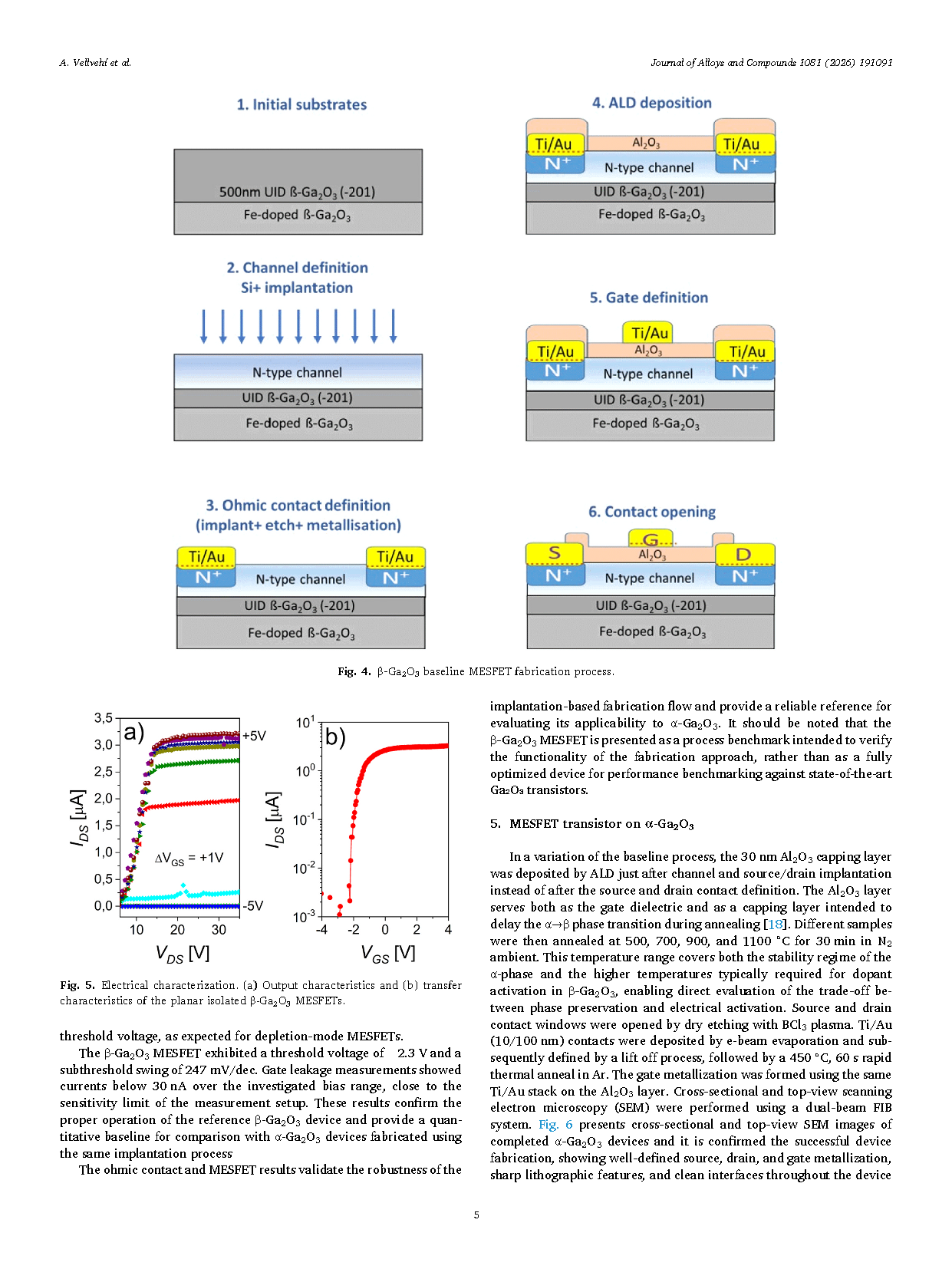
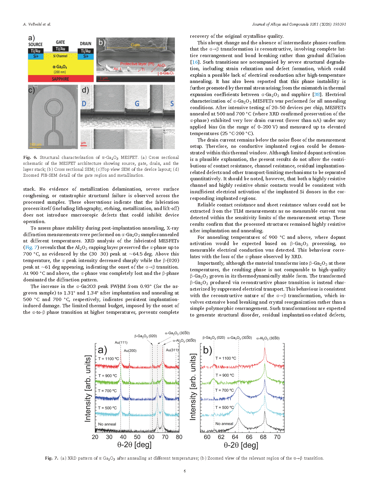
Ion-implantation-based channel engineering in α-Ga₂O₃ and β-Ga₂O₃ is investigated using an analogous Si-implanted lateral MESFET fabrication process for both polymorphs. In β-Ga₂O₃, silicon implantation defines both the conductive channel and the ohmic contact regions. This is achieved through multi-energy Si plantations (10, 30, 60, 95, and 200 keV) using total doses of 2 × 10¹³ cm⁻² for the channel region and 2 × 10¹⁵ cm⁻² for the contact regions, followed by annealing at 900–1100 °C, resulting in well-defined conductive channels and contacts. Although this implantation-annealing approach is effective for conductivity control in unintentionally doped (UID) β-Ga₂O₃ layers grown on Ga₂O₃ or sapphire, it remains problematic for thermally metastable α-Ga₂O₃. To mitigate this limitation, an atomic layer deposited (ALD) Al₂O₃ capping layer is introduced to enhance the thermal stability of corundum-phase α-Ga₂O₃ on m-plane sapphire during post-implantation annealing (500–1100 °C). The capping layer increases the α-phase stability, delaying the α → β transition to approximately 700 °C, well above the threshold observed in uncapped films. Despite this improvement, electrical measurements indicate that such temperatures are still insufficient to obtain a sufficiently conductive implanted region. At higher annealing temperatures, where efficient activation would normally be expected, the material undergoes complete transformation to the β phase, introducing additional structural disorder and preventing effective device operation. In this context, low-thermal-budget activation techniques such as pulsed laser annealing (PLA) and flash lamp annealing (FLA) may represent promising alternatives. These approaches can generate very high transient surface temperatures while maintaining a much lower average thermal load on the material. As a result, dopant activation and implantation-damage recovery may occur on timescales shorter than those required for the extensive atomic rearrangements associated with the reconstructive α → β phase transformation. Consequently, localized transient annealing could potentially improve electrical activation while preserving the α-Ga₂O₃ crystal structure. Although this hypothesis remains to be experimentally verified, such approaches may provide a viable pathway to overcome the thermal-budget limitations identified in the present work. These results indicate that conventional ion-implantation activation strategies developed for β-Ga₂O₃ are fundamentally incompatible with metastable α-Ga₂O₃, even when thermal stabilization layers are employed. Beyond demonstrating this limitation, the present work establishes a practical benchmark for implantation-based α-Ga₂O₃ device fabrication.
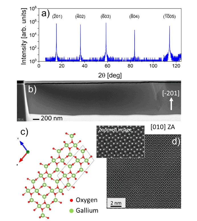
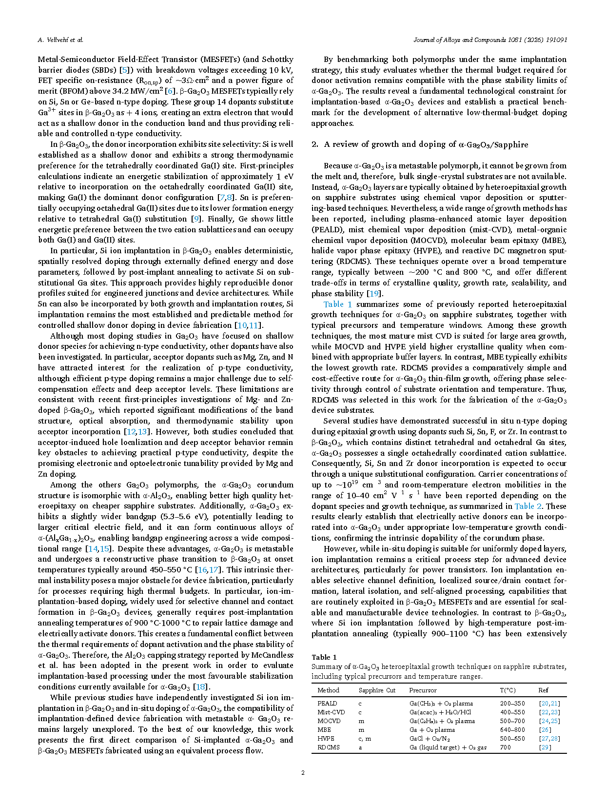
Fig. 1. Structural analysis of β-Ga₂O₃ homoepitaxially grown on (-201) Ga₂O₃: Fe substrate. (a) XRD scan, (b) HAADF-TEM image of the FIB prepared lamella, (c) VESTA simulation of a β-Ga₂O₃ crystal with [010] zone axis, and (d) HAADF-TEM image with atomic resolution of the Ga columns.
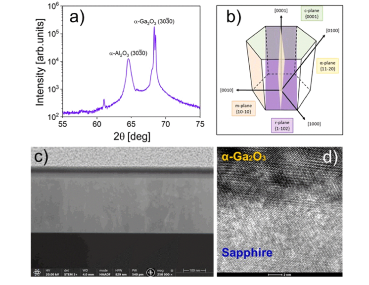
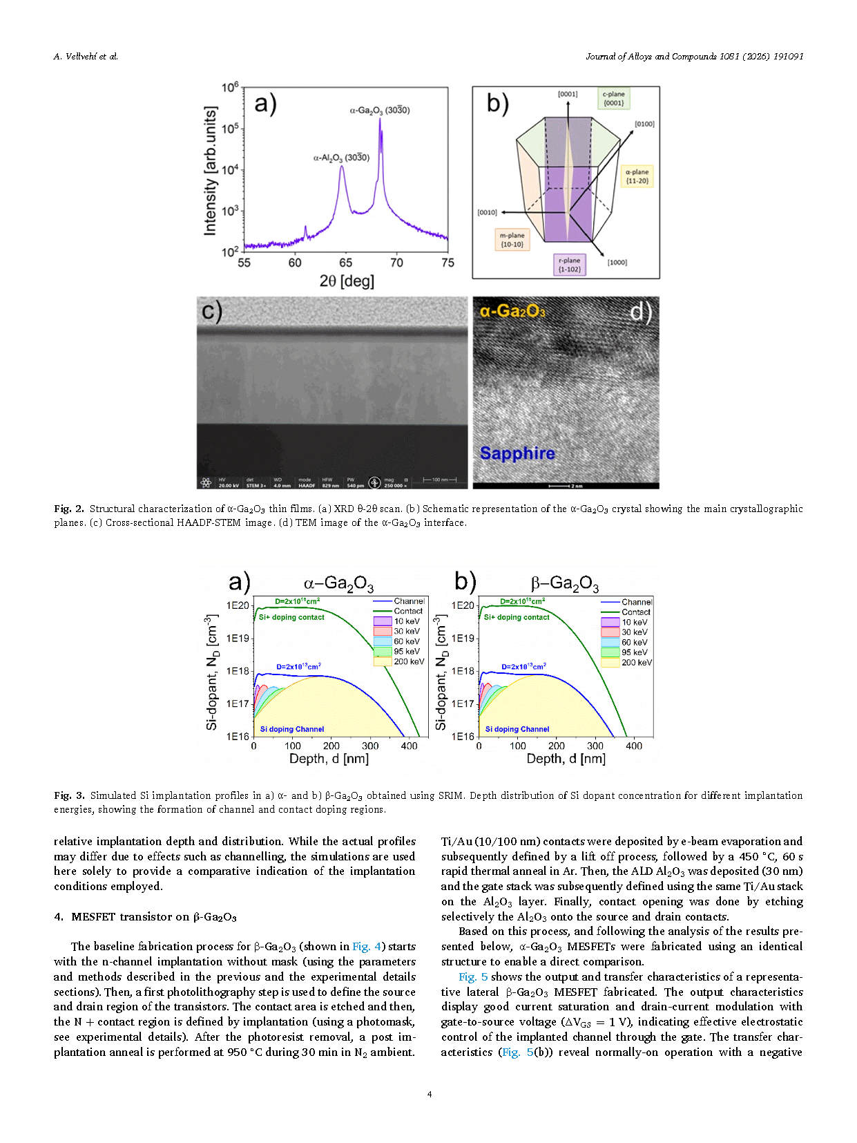
Fig. 2. Structural characterization of α-Ga₂O₃ thin films. (a) XRD θ-2θ scan. (b) Schematic representation of the α-Ga₂O₃ crystal showing the main crystallographic planes. (c) Cross-sectional HAADF-STEM image. (d) TEM image of the α-Ga₂O₃ interface.
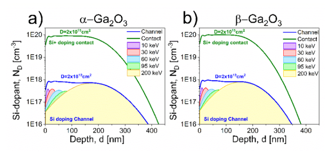
Fig. 3. Simulated Si implantation profiles in a) α- and b) β-Ga₂O₃ obtained using SRIM. Depth distribution of Si dopant concentration for different implantation energies, showing the formation of channel and contact doping regions.
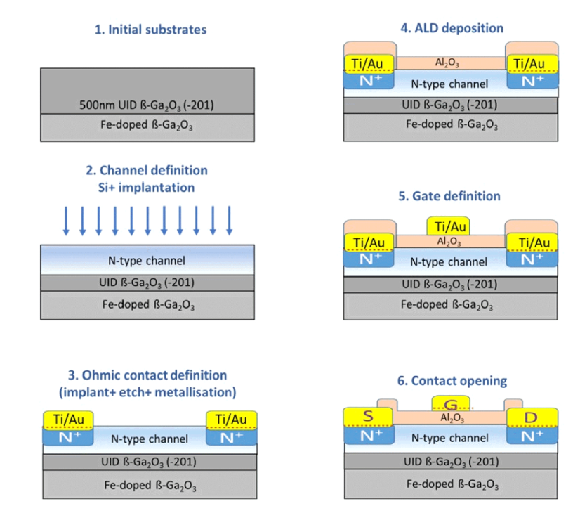
Fig. 4. β-Ga₂O₃ baseline MESFET fabrication process.
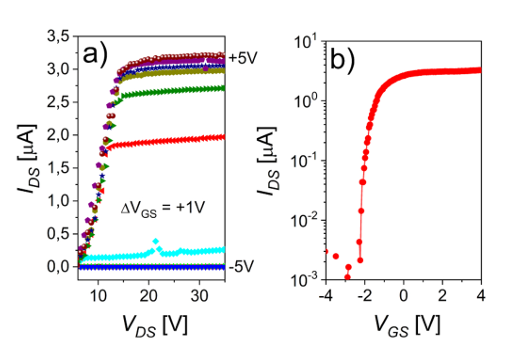
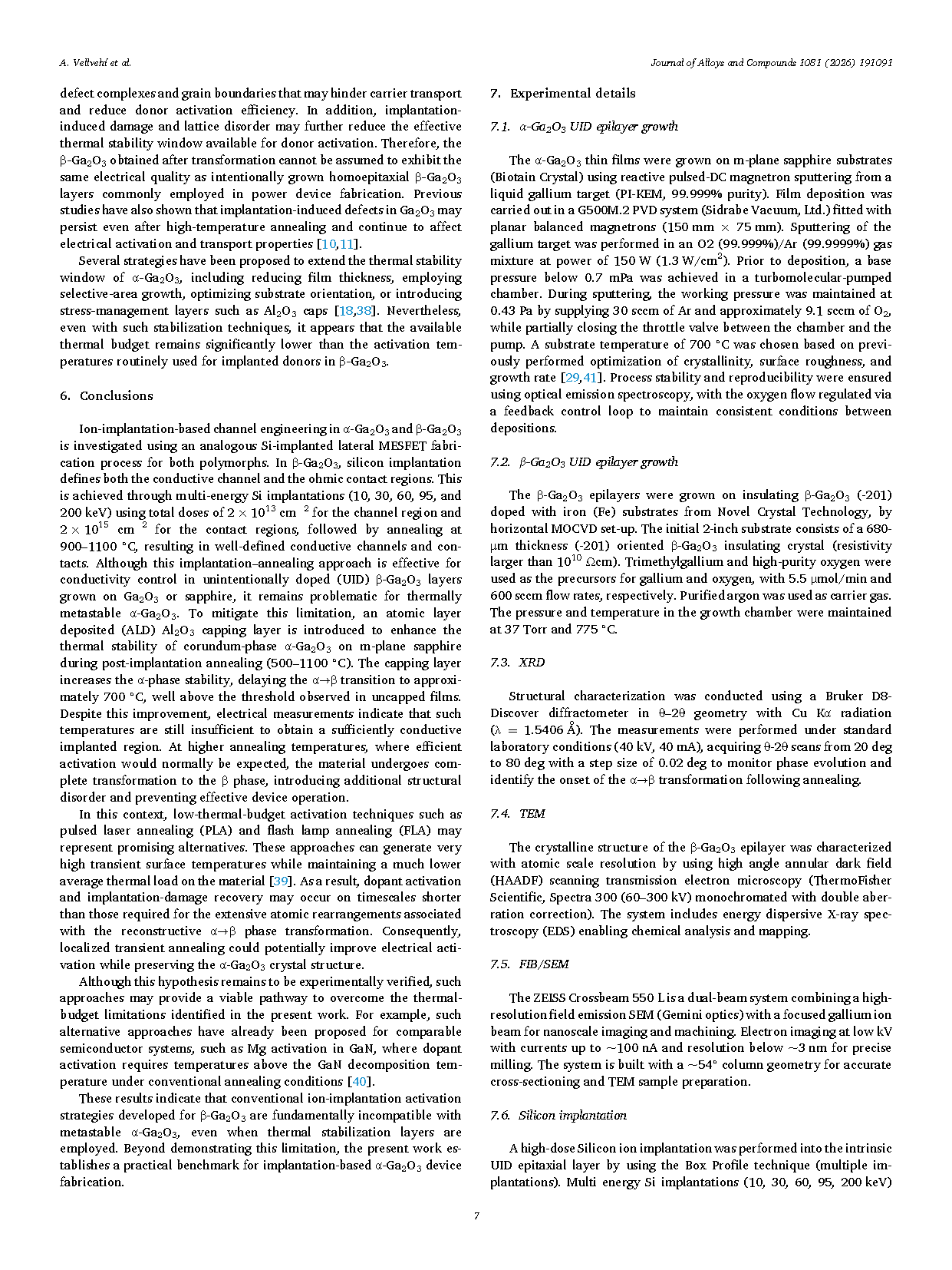
Fig. 5. Electrical characterization. (a) Output characteristics and (b) transfer characteristics of the planar isolated β-Ga₂O₃ MESFETs.
DOI:
doi.org/10.1016/j.jallcom.2026.191091
Instruction
Official Account

Cooperation
Top
