


Researchers from the Yongjiang Laboratory have published a dissertation titled "Atomic-Scale Strain Relaxation via Ar-Bombarded Surface Modification for Enabling Single-Crystalline β-Ga₂O₃ (010) Heteroepitaxy" in Nano Letters.
Background
The ultrawide bandgap semiconductor gallium oxide (Ga₂O₃) has emerged as a promising candidate for high-power electronics and solar-blind optoelectronic devices. Among the known Ga₂O₃ polymorphs, the monoclinic β-phase is thermodynamically the most stable. The feasible ntype doping and high breakdown field strength render it competitive for high-voltage power switching. Besides, the rapid development of large-scale and high-quality β-Ga₂O₃ single-crystal substrates facilitates steady advance of β-Ga₂O₃- based power devices. Among the commonly investigated orientations, β-Ga₂O₃ with the (010) orientation exhibits higher thermal conductivity and faster epitaxial growth rates compared to those with other orientations. Furthermore, β-Ga₂O₃ vertical Schottky barrier diodes (SBDs) with the (010) orientation demonstrate much reduced reverse leakage current and enhanced breakdown voltage, since the drift layer in this orientation exhibits a lower surface defect density and could enable a more ideal Schottky contact. Despite advances in homoepitaxial growth of (010)-oriented β-Ga₂O₃ films, a critical roadblock persists in obtaining largescale (010)-oriented β-Ga₂O₃ single-crystal substrates with a diameter over 2 inch. This is due to the growth challenges of defect suppression at this orientation and the cleavage problem during the wafer thinning and polishing process. On the other hand, using foreign substrates to obtain (010)-oriented phase-pure β-Ga₂O₃ films appears to be an alternative solution, but is hindered by severe lattice mismatch during the heteroepitaxy growth. For example, while the sapphire substrate orientation is found effective to dictate the selective phase formation of Ga₂O₃, the (010)-oriented β-Ga₂O₃ is only seen as randomly distributed impurity phase in the growth of α-Ga₂O₃ films as a result of strain-relaxed phase transition.
Abstract
Gallium oxide (Ga2O3) is an emerging ultrawide bandgap semiconductor for high-power electronics and solar-blind optoelectronics. Here we demonstrate an atomic-scale strain relaxation method to achieve a complete α-to-β Ga2O3 phase transition within the initial nucleation stage, enabling a heteroepitaxial growth regime of single-crystalline β-Ga2O3 (010) films. An Ar+ bombardment strategy is used to create periodic strain relaxation sites that relieve the compressive strain in the metastable α-Ga2O3 interlayer and facilitate the phase transition, as revealed by a combination of X-ray diffraction, atomic-force microscopy, atomic-resolution scanning transmission electron microscopy, and geometric phase analysis. The heteroepitaxial Sn-doped β-Ga2O3 (010) films with distinct donor activation behavior are established on m-plane sapphire, and a lateral Schottky barrier diode with a high reverse breakdown voltage of 1590 V is achieved. This study provides critical insights into atom-scale strain engineering and confined epitaxial growth for developing high-quality β-Ga2O3 films on cost-effective substrates for advanced electronic devices.
Highlights
By bombarding m-face sapphire with Ar⁺ ions, atomic-scale control of the substrate surface was achieved, providing a new method for interface engineering in β-Ga₂O₃ heteroepitaxy.
The formation of an ultrathin α-Ga₂O₃ transition layer at the β-Ga₂O₃/sapphire interface was revealed; this layer is capable of accommodating interfacial strain and facilitating rapid strain release.
Through atomically resolved STEM, GPA strain analysis and EELS characterization, the relationship between interfacial strain control, the formation of α-Ga₂O₃ and its transformation into β-Ga₂O₃ was elucidated.
Following optimization of the Ar⁺ bombardment conditions, phase-pure (010) β-Ga₂O₃ films were achieved, providing a new route for the epitaxial growth of high-quality gallium oxide on low-cost substrates.
Conclusion
In summary, this study demonstrates an atomic-scale strain relaxation method to achieve single-crystalline β-Ga₂O₃ (010) heteroepitaxy. In contrast to the conventional observation of the α-Ga₂O₃ film growth on m-plane sapphire, an Ar+ bombardment treatment on the sapphire substrate effectively modifies the phase evolution route and forms a high-quality, homogeneous (010) β-Ga₂O₃ film. Combined analysis of XRD, AFM, STEM/EELS and GPA reveals that the surface treatment introduces periodic surface sites for compressive strain relaxation on the initial α-Ga₂O₃ nucleation layer that leads to abrupt α-Ga₂O₃ to β-Ga₂O₃ phase transition within the nanometer thickness. The β-Ga₂O₃ (010) heteroepitaxy with a higher growth rate is established that exhibits a FWHM of 0.59° on m-plane sapphire. This strain-relaxation method supports the growth of heteroepitaxial (010) β-Ga₂O₃ films with distinct donor activation behavior, and a lateral Schottky barrier diode with a reverse breakdown voltage of 1590 V is demonstrated. This study reveals the critical role of atomic-scale strain engineering in expanding the epitaxial paradigm for advanced electronic devices.
Project Support
This work was supported by National Natural Science Foundation of China (Grant No. 62304227), the China Postdoctoral Science Foundation (Grant No. 2025M773410), the Zhejiang Provincial Natural Science Foundation of China (Grant Nos. LQN26F040002 and LQ23F040005), and the Ningbo Yongjiang Talent Introduction Programme (Grant No. 2021A-046-C).
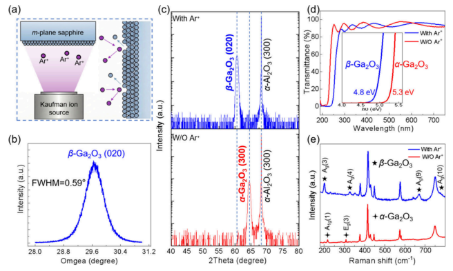
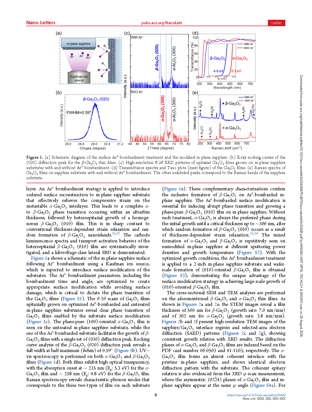
Figure 1. (a) Schematic diagram of the surface Ar+ bombardment treatment and the modified m-plane sapphire. (b) X-ray rocking curves of the (020) diffraction peak for the β-Ga2O3 thin films. (c) High-resolution θ-2θ XRD patterns of epitaxial Ga2O3 films grown on m-plane sapphire substrates with and without Ar+ bombardment. (d) Transmittance spectra and Tauc plots (inset figure) of the Ga2O3 films. (e) Raman spectra of Ga2O3 films on sapphire substrate with and without Ar+ bombardment. The other unlabeled peaks correspond to the Raman bands of the sapphire substrate.
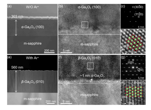
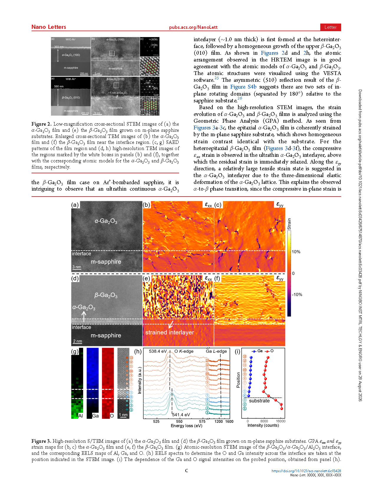
Figure 2. Low-magnification cross-sectional STEM images of (a) the α-Ga2O3 film and (e) the β-Ga2O3 film grown on m-plane sapphire substrates. Enlarged cross-sectional TEM images of (b) the α-Ga2O3 film and (f) the β-Ga2O3 film near the interface region. (c, g) SAED patterns of the film region and (d, h) high-resolution TEM images of the regions marked by the white boxes in panels (b) and (f), together with the corresponding atomic models for the α-Ga2O3 and β-Ga2O3 films, respectively.
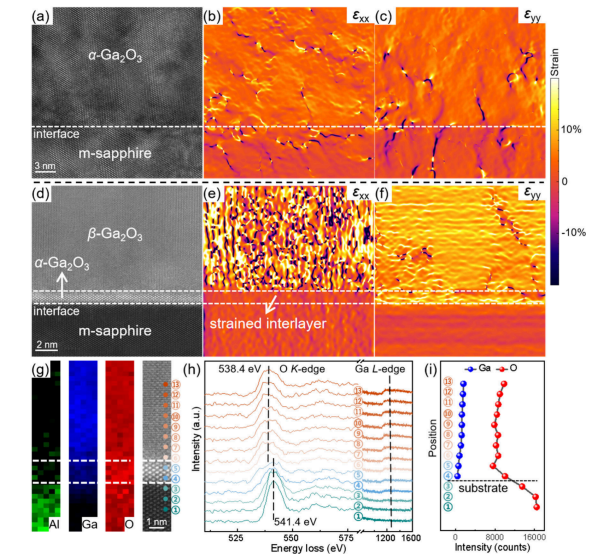
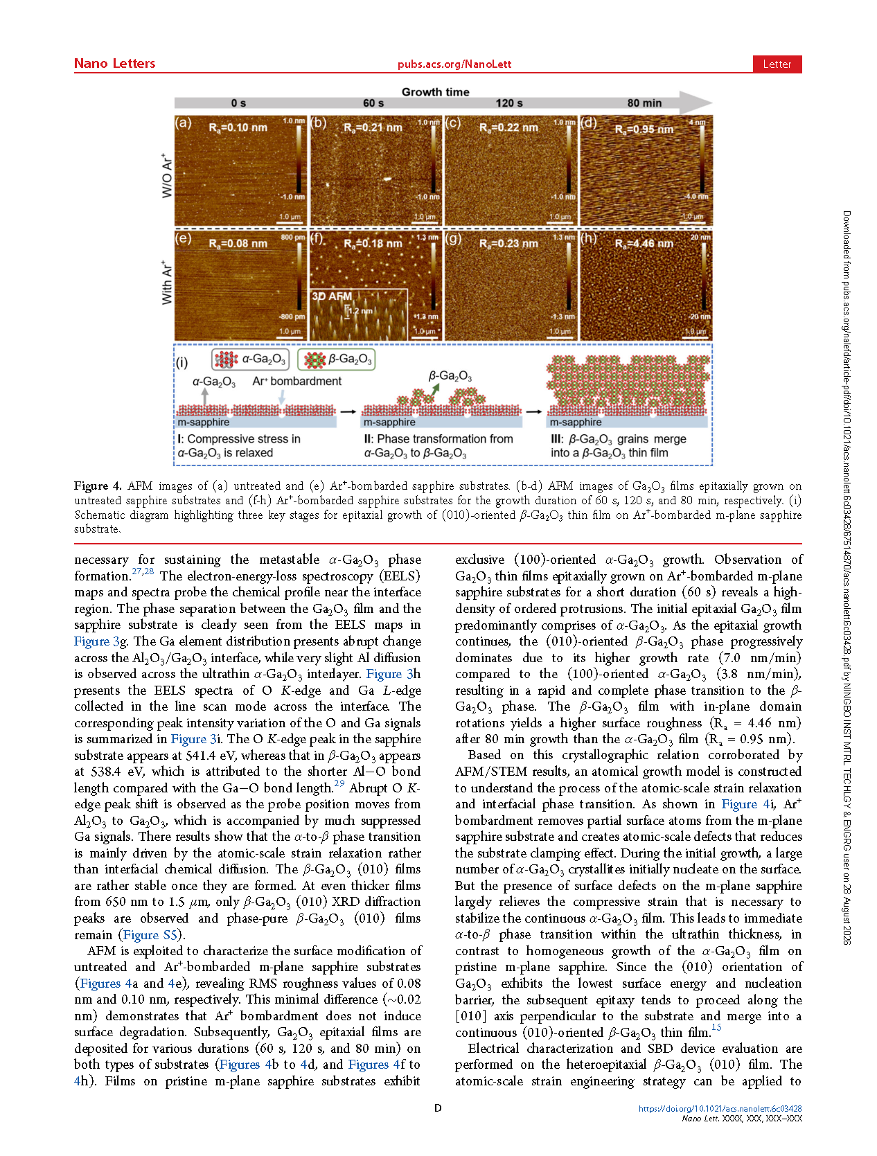
Figure 3. High-resolution S/TEM images of (a) the α-Ga2O3 film and (d) the β-Ga2O3 film grown on m-plane sapphire substrates. GPA εxx and εyy strain maps for (b, c) the α-Ga2O3 film and (e, f) the β-Ga2O3 film. (g) Atomic-resolution STEM image of the β-Ga2O3/α-Ga2O3/Al2O3 interface, and the corresponding EELS maps of Al, Ga, and O. (h) EELS spectra to determine the O and Ga intensity across the interface are taken at the position indicated in the STEM image. (i) The dependence of the Ga and O signal intensities on the probed position, obtained from panel (h).
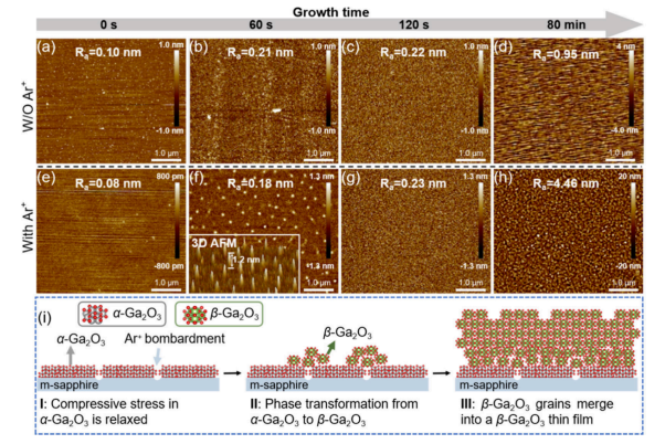
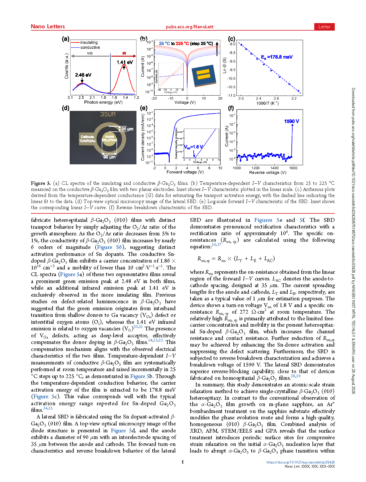
Figure 4. AFM images of (a) untreated and (e) Ar⁺ -bombarded sapphire substrates. (b-d) AFM images of Ga2O3 films epitaxially grown on untreated sapphire substrates and (f-h) Ar⁺ -bombarded sapphire substrates for the growth duration of 60 s, 120 s, and 80 min, respectively. (i) Schematic diagram highlighting three key stages for epitaxial growth of (010)-oriented β-Ga2O3 thin film on Ar+ -bombarded m-plane sapphire substrate.
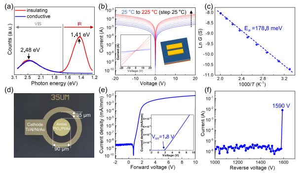
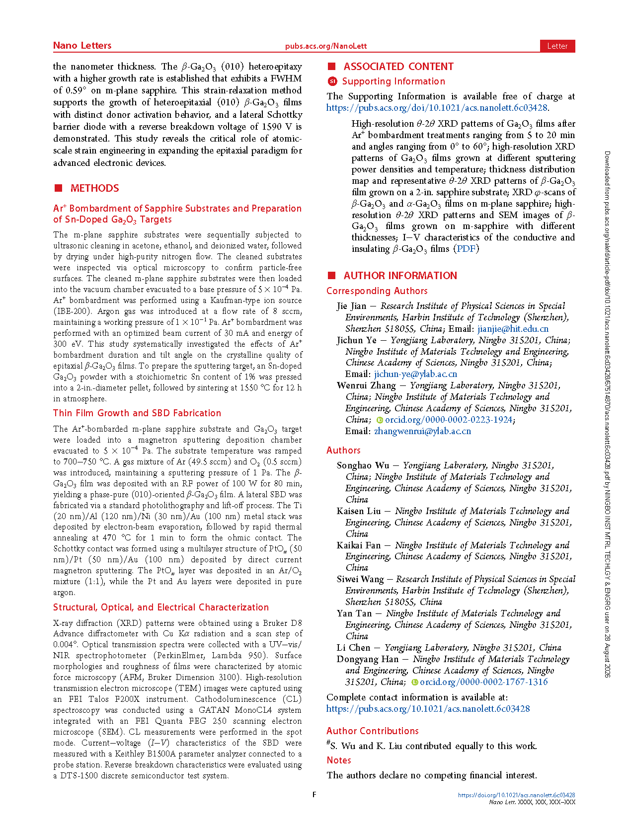
Figure 5. (a) CL spectra of the insulating and conductive β-Ga2O3 films. (b) Temperature-dependent I−V characteristics from 25 to 225 °C measured on the conductive β-Ga2O3 film with two planar electrodes. Inset shows I−V characteristic plotted in the linear scale. (c) Arrhenius plots derived from the temperature-dependent conductance (G) data for estimating the transport activation energy, with the dashed line indicating the linear fit to the data. (d) Top-view optical microscopy image of the lateral SBD. (e) Log-scale forward I−V characteristic of the SBD. Inset shows the corresponding linear I−V curve. (f) Reverse breakdown characteristic of the SBD.
DOI:
doi.org/10.1021/acs.nanolett.6c03428
Instruction
Official Account

Cooperation
Top
