


A research team led by Prof. Zheng Shi at Nanjing University of Posts and Telecommunications has published a study entitled “Self-Powered Programmable UV Optoelectronic Logic Gates via Polarity-Reversal Photocurrent in a Ga₂O₃/GaN Heterojunction” in Applied Physics Letters. By exploiting the polarity reversal of photocurrent in a Ga₂O₃/GaN heterojunction under different UV wavelengths, the work demonstrates multiple reconfigurable UV optoelectronic logic functions under zero-bias operation, providing a new device strategy for low-power UV sensing and information processing.
Background
With the rapid development of artificial intelligence and edge computing, the growing demand for data processing is placing increasing pressure on conventional electronic logic hardware in terms of power consumption, interconnect complexity, and system integration. In UV sensing and communication, in particular, there is a growing need for compact and energy-efficient logic devices capable of directly processing UV optical inputs.
Ultraviolet light features low background interference and high spectral selectivity, making it attractive for secure communication, environmental monitoring, space communication, and information encryption. Conventional optoelectronic information-processing systems generally require photodetectors to first convert optical signals into electrical signals, followed by separate electronic logic circuits for subsequent processing. Such a discrete “optical-electrical-logic” architecture inevitably increases hardware complexity and energy consumption.
Optoelectronic logic devices directly integrate optical inputs with logic operations, offering a promising route toward compact and low-power optical information-processing systems. In recent years, logic operations based on optical parameters such as wavelength, polarization, and intensity have attracted considerable attention. However, optoelectronic logic platforms that simultaneously combine UV sensitivity, self-powered operation, multiple logic functions in a single device, and reconfigurability remain relatively limited.
Wide-bandgap semiconductors provide an attractive material platform for UV optoelectronic logic. β-Ga₂O₃, with an ultrawide bandgap of approximately 4.9 eV, is particularly suitable for deep-UV and solar-blind UV detection. GaN, meanwhile, benefits from mature material growth and device fabrication technologies and exhibits favorable near-UV photoresponse. Integrating these two materials into a Ga₂O₃/GaN heterojunction can combine their complementary UV spectral responses while enabling self-powered photoelectric conversion at zero bias through the built-in electric field.
More importantly, 254 and 365 nm UV light exhibit distinctly different absorption regions and carrier-transport processes in the Ga₂O₃/GaN heterojunction, resulting in photocurrents with opposite polarities. By exploiting this wavelength-dependent photocurrent polarity reversal, different UV inputs can be directly encoded into distinct logic states, providing a physical basis for reconfigurable logic operations within a single optoelectronic device.
Therefore, a single-device platform capable of zero-bias operation and multiple logic functions based on wavelength-dependent photocurrent polarity offers significant potential for low-power and highly integrated UV optoelectronic information processing.
Abstract
In this work, the researchers developed a self-powered UV photodetector based on a β-Ga₂O₃/GaN heterojunction and further exploited the photocurrent polarity reversal induced by different UV wavelengths to realize programmable UV optoelectronic logic functions.
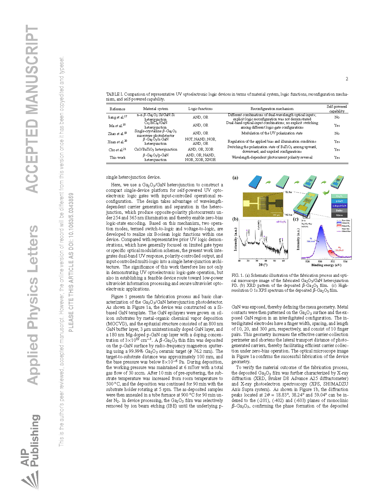
The Ga₂O₃/GaN heterojunction was fabricated on a Si-based GaN template. The GaN epitaxial structure consisted of an 800 nm GaN buffer layer, a 3 μm unintentionally doped GaN layer, and a 180 nm Mg-doped p-GaN layer. A β-Ga₂O₃ film was subsequently deposited on the p-GaN surface by radio-frequency magnetron sputtering. An interdigitated electrode configuration was employed to increase the carrier-collection perimeter and reduce the lateral transport distance of photogenerated carriers, thereby improving carrier collection under zero-bias operation. XRD and XPS characterization further confirmed the formation of the β-Ga₂O₃ film.
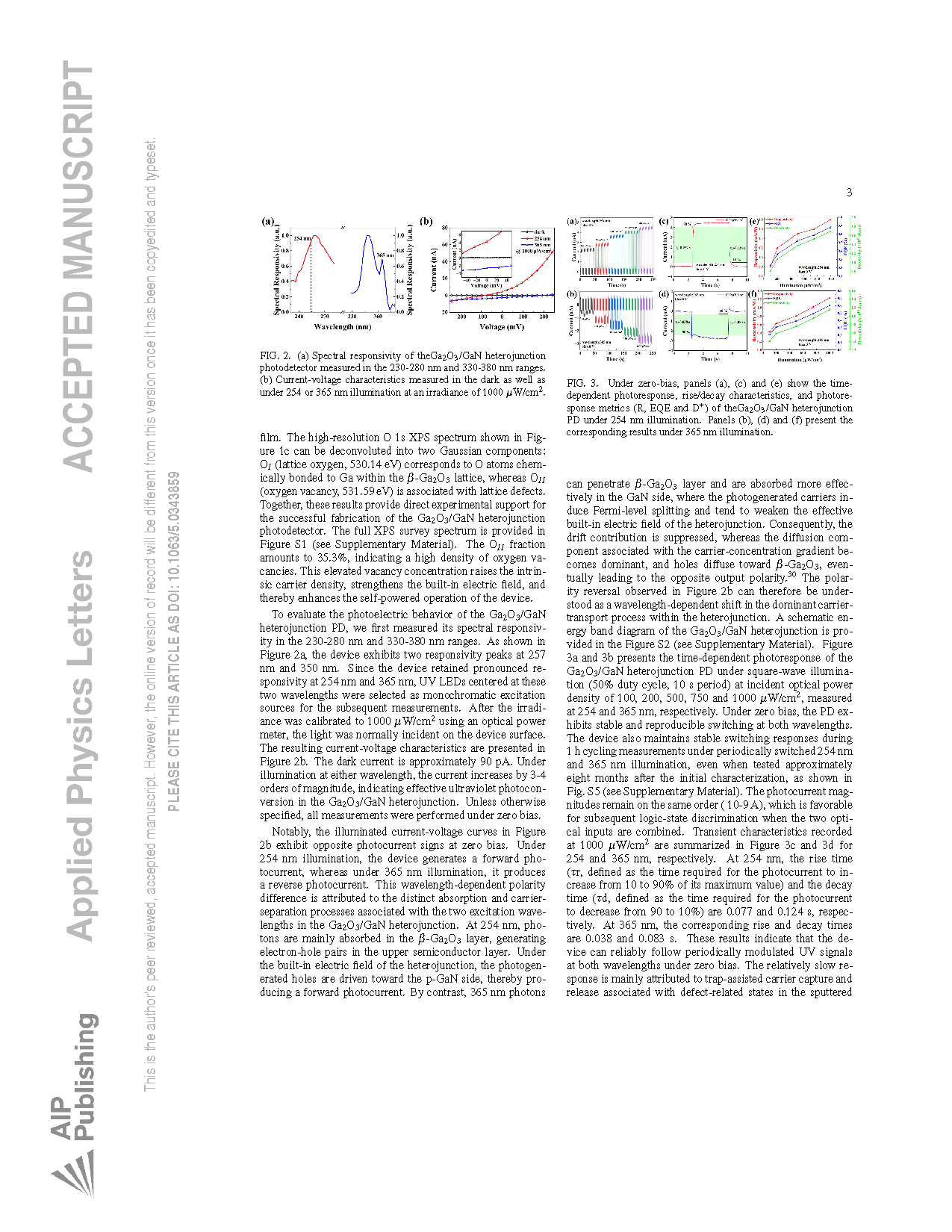
Spectral measurements revealed a distinct dual-peak UV response, with response peaks located at approximately 257 and 350 nm. Based on this characteristic, 254 and 365 nm were selected as the two UV inputs for subsequent logic operations. Under zero bias, the device exhibited a dark current of approximately 90 pA, while UV illumination at either 254 or 365 nm increased the device current by approximately three to four orders of magnitude.
A particularly notable feature is that the device generates photocurrents with opposite polarities under 254 and 365 nm illumination at the same zero-bias condition. Illumination at 254 nm produces a positive photocurrent, whereas 365 nm illumination generates a negative photocurrent.
This polarity reversal originates from the distinct optical absorption and carrier-transport mechanisms associated with the two wavelengths. The 254 nm photons are predominantly absorbed in β-Ga₂O₃, and the photogenerated carriers are driven by the built-in electric field of the heterojunction, producing a positive photocurrent. In contrast, 365 nm light can penetrate through β-Ga₂O₃ and generate photocarriers in the GaN region, modifying the effective built-in electric field and allowing diffusion to gradually dominate the transport process, ultimately resulting in a photocurrent with the opposite polarity.
Based on this wavelength-dependent photocurrent polarity reversal, the researchers further developed two complementary reconfigurable logic operation modes.
The first is the “Switch-to-Logic” mode. Two independently driven 254 and 365 nm UV LEDs serve as optical inputs, with the ON and OFF states of each LED defined as logic “1” and “0”, respectively. Logic states are then determined according to predefined thresholds of the output photocurrent. Using a single Ga₂O₃/GaN heterojunction device, AND, OR, and XOR operations were realized. By reversing the output logic assignment, the corresponding NAND, NOR, and XNOR functions were also obtained.
The second is the “Voltage-to-Logic” mode. Rather than simply using the ON/OFF states of the LEDs, the driving voltages of the 254 and 365 nm UV LEDs are employed as input variables. Taking advantage of the opposite photocurrent polarities associated with the two wavelengths, a two-dimensional output-photocurrent map was constructed. By selecting different input-voltage windows, NOR, NAND, OR, AND, and XNOR functions were realized, while XOR could be obtained by changing the logic assignment of the corresponding regions.
These two modes enable logic configuration through either optical switching states or driving-voltage windows, allowing multiple logic functions to be implemented in the same device without modifying its physical structure and providing a new route toward integrated UV sensing and logic processing.
Highlights
Integration of self-powered UV detection and logic operation: The built-in electric field of the Ga₂O₃/GaN heterojunction enables UV photoelectric conversion and logic operations at zero bias without an additional external bias voltage.
Photocurrent polarity reversal as a logic-encoding mechanism: The wavelength-dependent polarity reversal under 254 and 365 nm illumination directly links UV optical inputs, carrier transport, and logic outputs.
Six Boolean logic functions integrated in a single device: AND, OR, NAND, NOR, XOR, and XNOR functions are realized using a single Ga₂O₃/GaN heterojunction device, enhancing the functional integration of UV optoelectronic logic.
Two complementary reconfigurable logic modes: “Switch-to-Logic” uses the ON/OFF states of UV LEDs for logic operation, whereas “Voltage-to-Logic” enables logic reconfiguration by selecting different UV-LED driving-voltage windows, providing flexible routes toward multifunctional UV optoelectronic logic.
Conclusion
This work demonstrates a self-powered UV photodetector based on a Ga₂O₃/GaN heterojunction and exploits the photocurrent polarity reversal induced by 254 and 365 nm UV illumination to realize reconfigurable UV optoelectronic logic under zero-bias operation.
The study establishes the relationship between wavelength-dependent optical absorption, carrier-transport mechanisms, and photocurrent polarity, providing a direct physical basis for encoding UV optical signals into logic states. Through the complementary “Switch-to-Logic” and “Voltage-to-Logic” operation modes, six Boolean logic functions—AND, OR, NAND, NOR, XOR, and XNOR—are implemented in a single device. These results provide a promising device strategy for low-power, highly integrated UV sensing and logic processing.
Project Support
This work was jointly supported by the National Natural Science Foundation of China (62274096), Jiangsu Funding Program for Excellent Postdoctoral Talent (2025ZB868), and the Postdoctoral Fellowship Program of CPSF (GZB20250149).
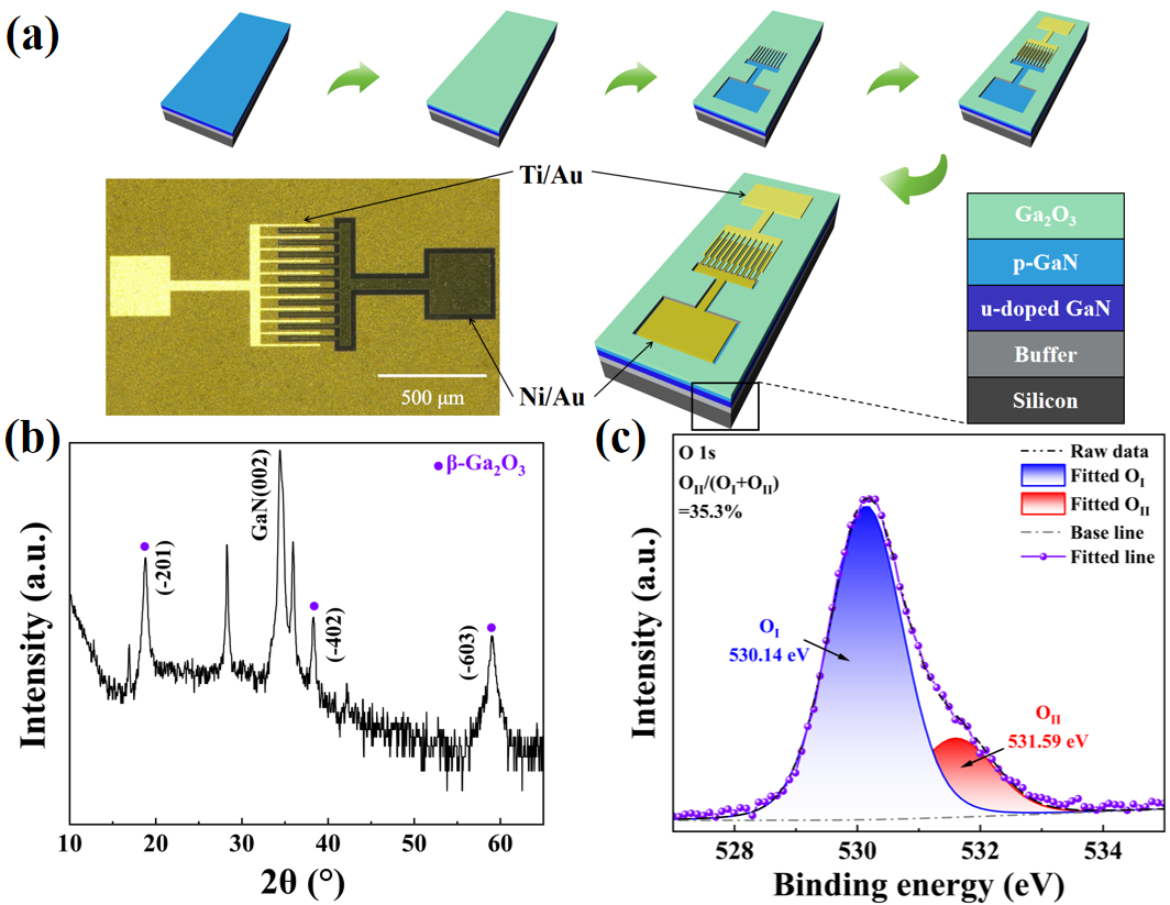
Figure 1. (a) Schematic illustration of the fabrication process and optical microscope image of the fabricated Ga₂O₃/GaN heterojunction PD. (b) XRD pattern of the deposited β-Ga₂O₃ film. (c) High-resolution O 1s XPS spectrum of the deposited β-Ga₂O₃ film.
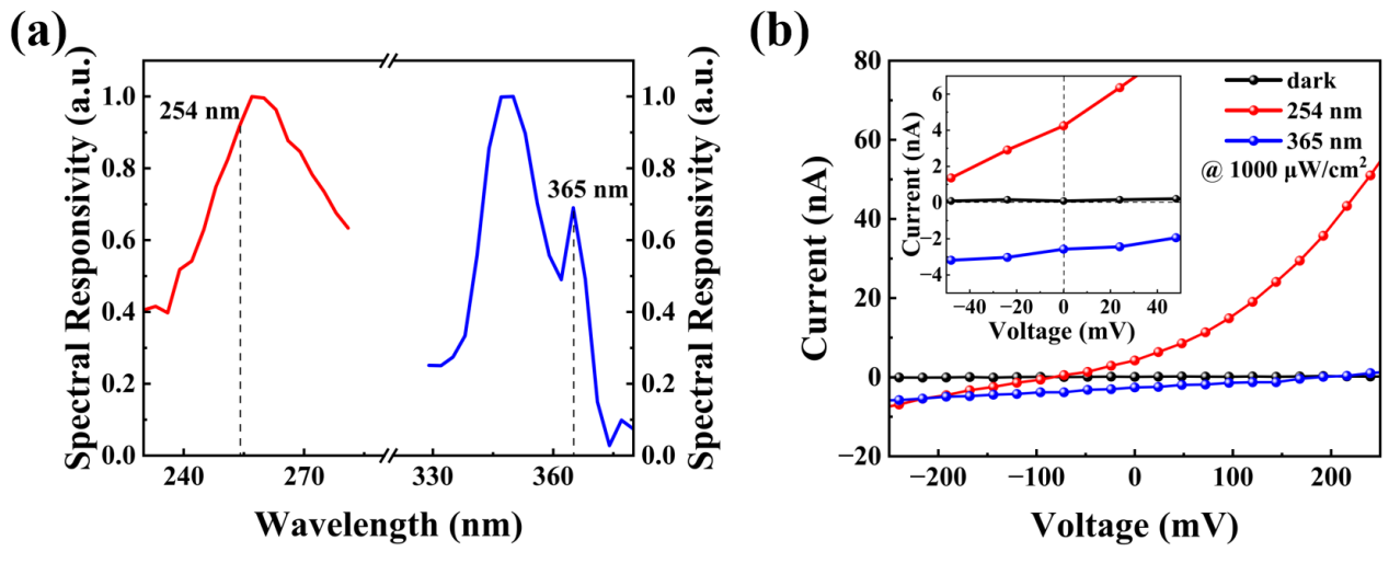
Figure 2. (a) Spectral responsivity of the Ga₂O₃/GaN heterojunction photodetector measured in the 230-280 nm and 330-380 nm ranges. (b) Current-voltage characteristics measured in the dark as well as under 254 or 365 nm illumination at an irradiance of 1000 μW/cm2.
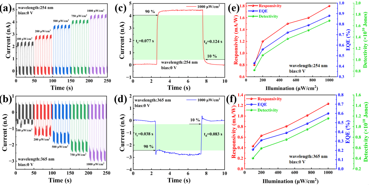
Figure 3. Under zero-bias, panels (a), (c) and (e) show the time-dependent photoresponse, rise/decay characteristics, and photoresponse metrics (R, EQE and D*) of the Ga₂O₃/GaN heterojunction PD under 254 nm illumination. Panels (b), (d) and (f) present the corresponding results under 365 nm illumination.
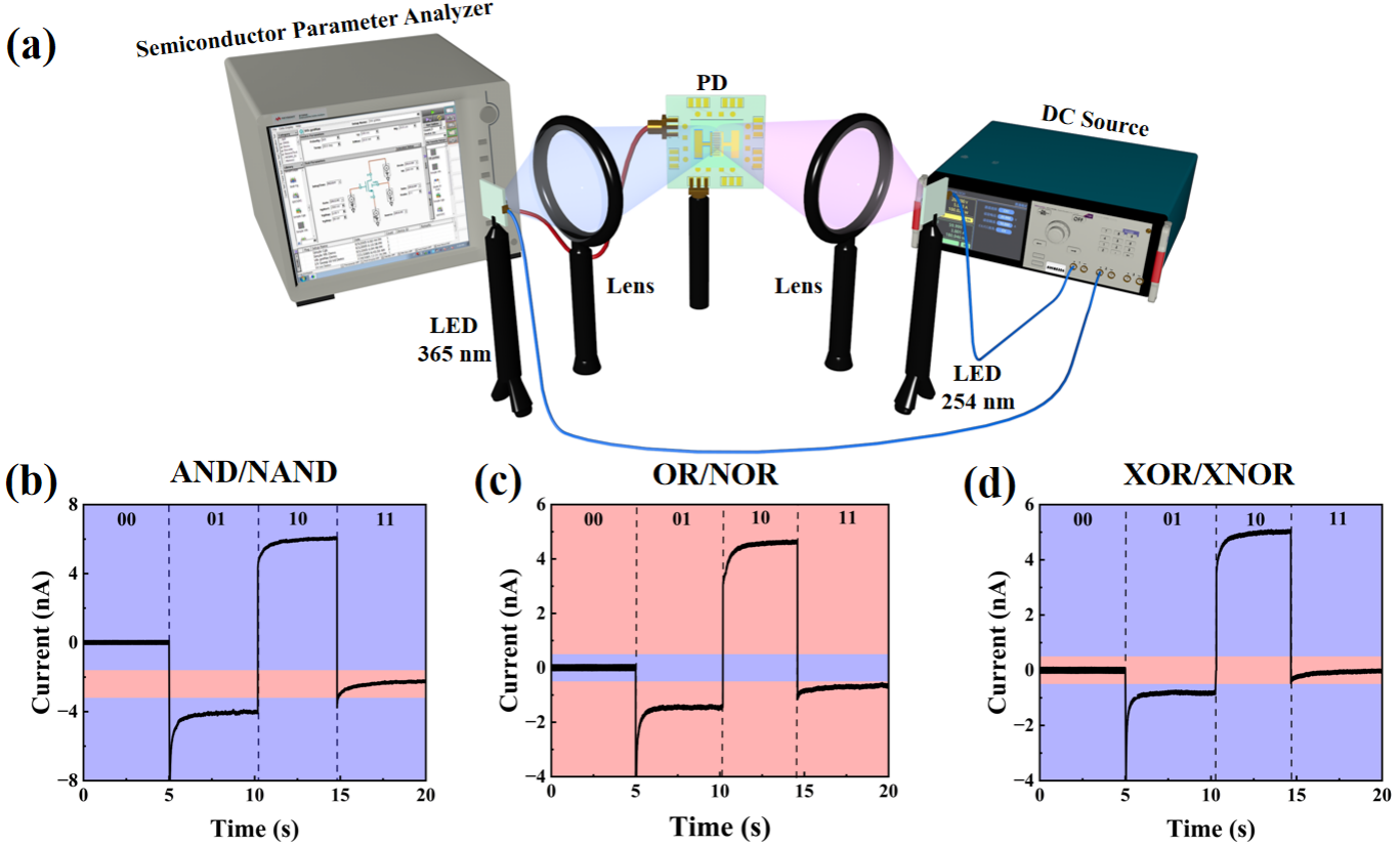
Figure 4. (a) Schematic of the experimental setup showing dual-LED illumination and photocurrent collection. Switch-to-logic verification of reconfigurable UV optoelectronic logic gates: (b) AND/NAND, (c) OR/NOR, (d) XOR/XNOR.
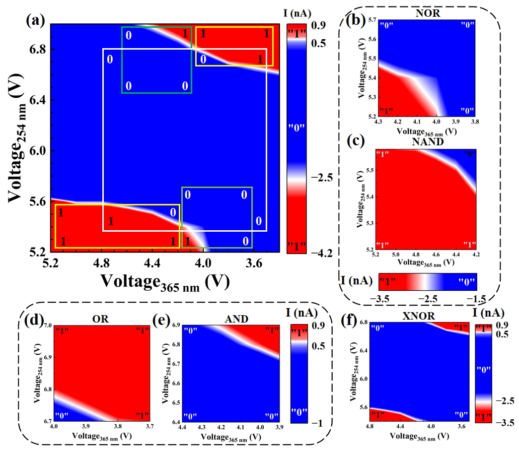
Figure 5. (a) Two-dimensional mapping of the output photocurrent as a function of the driving voltages applied to the 254 and 365 nm LEDs. Voltage-to-logic realization of reconfigurable UV optoelectronic logic gates: (b) NOR, (c) NAND, (d) OR, (e) AND, and (f) XNOR.
Team Introduction

First Author: Xumin Gao is an Associate Professor at the School of Communications and Information Engineering, Nanjing University of Posts and Telecommunications (NJUPT), where she also serves as a graduate supervisor. She has led several research projects funded by the National Natural Science Foundation of China and the Natural Science Foundation of Jiangsu Province. Her research interests focus on III-nitride optoelectronic devices and monolithically integrated visible light communication systems.

Corresponding Author: Zheng Shi is an Associate Professor and Vice Dean at the School of Communications and Information Engineering, Nanjing University of Posts and Telecommunications (NJUPT), where he also serves as a graduate supervisor. He has led several research projects funded by the National Natural Science Foundation of China (General Program and Youth Science Fund) and the Natural Science Foundation of Jiangsu Province. His research interests focus on wireless optical communication systems and key optoelectronic devices.
DOI:
doi.org/10.1063/5.0343859
Instruction
Official Account

Cooperation
Top
