


When Ga₂O₃ is discussed, high-voltage power devices are often among the first applications to attract attention. In the United States, however, an R&D project led by Rocky Mountain National Laboratory, formerly known as the U.S. National Renewable Energy Laboratory, is taking oxide electronic devices further into extreme operating environments where high temperature, high pressure, corrosive atmospheres, and mechanical stress coexist, exploring their potential applications in areas including energy, manufacturing, transportation, geothermal systems, and data centers.
The focus of this work is not simply to develop a particular type of device, but to establish a complete technology pathway covering materials, epitaxy, device fabrication, and reliability validation under extreme operating conditions.
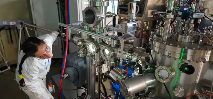
Image caption: Rocky Mountain National Laboratory, photographed by Brooks Tellekamp. Drawing on its expertise in materials science, the laboratory is advancing the development of high-temperature, high-power electronic devices.
Why Bring Electronic Devices into “Extreme Environments”?
Electronic devices designed to operate at room temperature and under conventional power conditions often face challenges such as degraded material performance, reduced device reliability, and shortened service life when exposed to high temperatures, high pressures, or corrosive environments.
Yet in many energy and industrial applications, electronic devices must operate directly under these complex conditions.
For example, downhole monitoring in geothermal wells requires devices capable of withstanding high temperatures over extended periods. Industrial manufacturing processes may involve high temperature, high power, and corrosive atmospheres simultaneously, while emerging transportation and energy systems are placing increasingly demanding requirements on high-power, highly reliable power electronics.
As a result, electronic devices capable of maintaining stable operation under extreme environmental conditions have become an important technological requirement for advanced energy systems and industrial equipment.
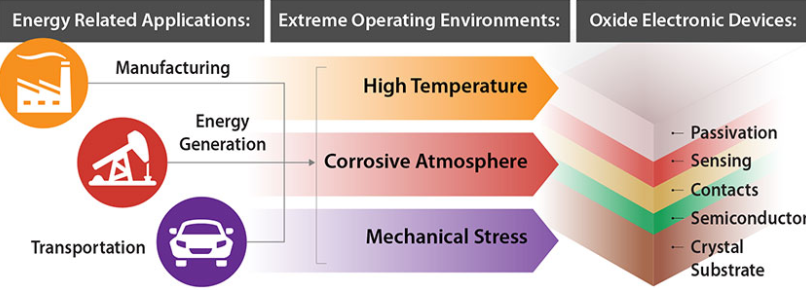
Figure caption: This project aims to develop oxide electronic devices incorporating a passivation layer, sensing layer, electrode contact layer, semiconductor layer, and crystalline substrate to meet the demands of high-power, high-temperature operation and other extreme conditions encountered in advanced energy, manufacturing, and grid-scale applications. Graphic by Al Hicks, Rocky Mountain National Laboratory.
From Ga₂O₃ Wafers to the Full Device Technology Chain
The project centers on oxide electronic devices, with a focus on advancing multiple stages along the technology pathway from materials to devices.
The first step is the development of single-crystal Ga₂O₃ wafers. The project aims to strengthen domestic U.S. manufacturing capabilities for single-crystal Ga₂O₃ wafers, providing a materials foundation for subsequent epitaxy and device development.
Building on this foundation, the research team will further develop semiconductor epitaxial layers, exploring epitaxial materials capable of operating under high-voltage and high-temperature conditions. The project will then move into device fabrication and sensor development, using the optimized wafers and epitaxial materials to develop oxide semiconductor devices and sensors.
Finally, the devices will undergo testing under conditions including high temperature, high pressure, corrosive atmospheres, and mechanical stress to evaluate their performance and reliability.
In other words, the R&D effort covers not just a single material or device, but a complete technology chain:
Crystal Substrate → Epitaxial Layer → Device Structure → Sensor → Extreme-Environment Testing → Reliability Validation
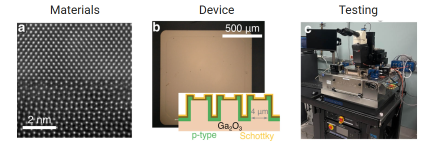
Figure caption: The Rocky Mountain National Laboratory capabilities utilized in this project include materials synthesis and characterization with atomically precise interfaces; electronic device fabrication and validation (shown is a top-view photograph of a microelectronic device with etched trenches); and characterization, modeling and simulation, and AI algorithm development using high-voltage probe stations. Micrograph (a) of the Ga₂O₃ interface photographed by Michelle Smeaton, Rocky Mountain National Laboratory; schematic illustration by Brooks Tellekamp.
Beyond Power Devices, What Else Can Ga₂O₃ Be Used For?
As R&D efforts move beyond the materials and devices themselves and into real-world operating conditions, the project is exploring application areas that extend beyond conventional power devices.
In the energy sector, the devices under development are being explored for energy conversion and high-power power electronics systems.
In geothermal applications, high-temperature electronic devices and sensors can be used for downhole environmental monitoring.
In manufacturing, the project focuses on the need for electronic monitoring and control in high-temperature, high-power industrial processes.
In transportation, the research covers potential power electronics applications in next-generation transportation systems.
The project also encompasses scenarios such as data-center power supplies and mineral extraction and processing.
One particularly notable direction is high-temperature sensing. Related research within the project has already explored hydrogen sensors, with efforts to improve their operating temperature and service life through materials and device design.
Materials, Devices, and Testing Capabilities Advancing in Parallel
The development of electronic devices for extreme environments places demands on materials fabrication and device testing that differ significantly from those for conventional electronic devices.
In this area, the project team brings together capabilities in atomically precise materials synthesis and characterization of interfaces, electronic device fabrication, high-voltage testing, modeling and simulation, and AI-assisted performance and reliability validation.
The project is also being carried out in collaboration with universities and industry partners. Academic collaborators include teams in metallurgical and materials engineering at the Colorado School of Mines. Industry partners include Luxium Technologies Solutions, which has capabilities in crystal growth and wafer manufacturing, and Kyma Technologies, which specializes in epitaxial growth processes and equipment.
The project has received funding and access to research facilities from the U.S. Department of Energy’s Office of Advanced Materials and Manufacturing Technologies.
From “Can It Be Done?” to “Can It Operate Reliably Under Extreme Conditions?”
Compared with simply pursuing performance metrics such as device voltage and current, electronic devices designed for extreme environments face another fundamental question: How long can a device continue to operate under real-world, complex operating conditions?
For this reason, the project has incorporated reliability assessment and accelerated validation into its R&D framework. It is also exploring the use of artificial intelligence to accelerate the analysis of device performance and reliability, aiming to develop validation methods for the long-term reliable operation of devices such as diodes and transistors.
Meanwhile, the U.S. Department of Energy (DOE) has previously supported multiple projects in related areas, including 20 kV Ga₂O₃ power devices, wide-bandgap power electronics, reliability validation of Ga₂O₃ semiconductor gas sensors, and oxide electronic devices for extreme environments.
When Ga₂O₃ Enters More Complex Operating Environments
From conventional high-voltage power devices to high-temperature sensors, downhole geothermal monitoring, and electronic equipment operating in complex industrial environments, the R&D landscape for Ga₂O₃ and other oxide semiconductors is expanding into increasingly demanding operating conditions.
For the Ga₂O₃ industry, this means that the advantages of the material will ultimately need to be demonstrated not only through electrical performance metrics in the laboratory, but also through wafer manufacturing, epitaxial quality, device processing, packaging, and reliability under extreme operating conditions.
The R&D effort led by a national laboratory provides a noteworthy overseas example: as operating environments evolve from “high voltage” to conditions involving high temperature, high pressure, corrosive atmospheres, and mechanical stress simultaneously, oxide electronic devices will need to address not only individual device-performance challenges, but also the development of an integrated materials–devices–reliability technology system.
This is another challenge that Ga₂O₃ will need to address as it moves from laboratory performance metrics toward real-world applications.
Instruction
Official Account

Cooperation
Top
