


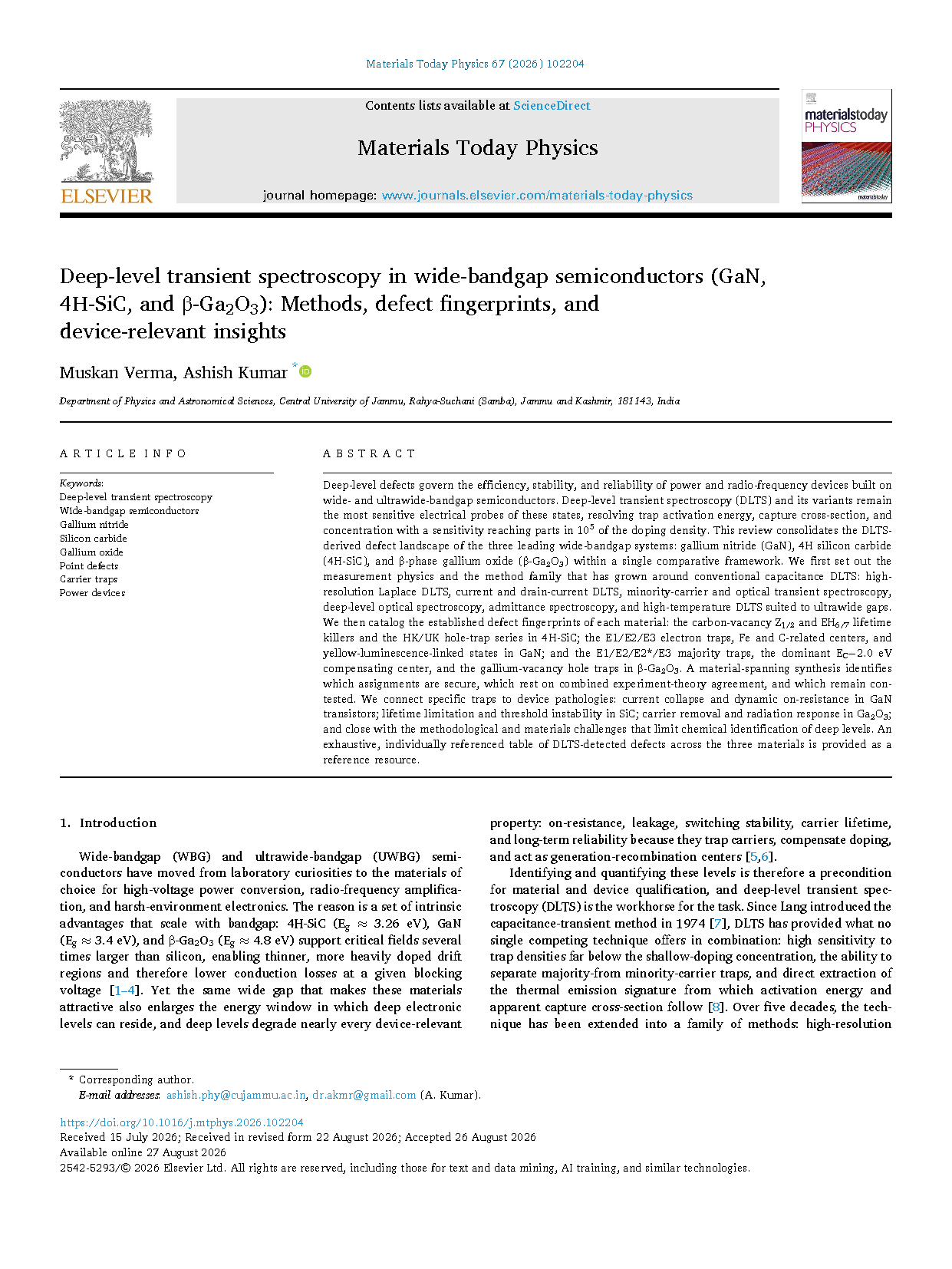
Researchers from Central University of Jammu have published a dissertation titled " Deep-Level Transient Spectroscopy in Wide-Bandgap Semiconductors (GaN, 4H-SiC, and β-Ga₂O₃): Methods, Defect Fingerprints, and Device-Relevant Insights " in Materials Today Physics.
Background
Wide-bandgap (WBG) and ultrawide-bandgap (UWBG) semiconductors have moved from laboratory curiosities to the materials of choice for high-voltage power conversion, radio-frequency amplification, and harsh-environment electronics. The reason is a set of intrinsic advantages that scale with bandgap: 4H-SiC (Eg≈3.26 eV), GaN (Eg≈3.4 eV), and β-Ga₂O₃ (Eg≈4.8 eV) support critical fields several times larger than silicon, enabling thinner, more heavily doped drift regions and therefore lower conduction losses at a given blocking voltage. Yet the same wide gap that makes these materials attractive also enlarges the energy window in which deep electronic levels can reside, and deep levels degrade nearly every device-relevant property: on-resistance, leakage, switching stability, carrier lifetime, and long-term reliability because they trap carriers, compensate doping, and act as generation-recombination centers.
Abstract
Deep-level defects govern the efficiency, stability, and reliability of power and radio-frequency devices built on wide- and ultrawide-bandgap semiconductors. Deep-level transient spectroscopy (DLTS) and its variants remain the most sensitive electrical probes of these states, resolving trap activation energy, capture cross-section, and concentration with a sensitivity reaching parts in 105 of the doping density. This review consolidates the DLTS-derived defect landscape of the three leading wide-bandgap systems: gallium nitride (GaN), 4H silicon carbide (4H-SiC), and β-phase gallium oxide (β-Ga₂O₃) within a single comparative framework. We first set out the measurement physics and the method family that has grown around conventional capacitance DLTS: high-resolution Laplace DLTS, current and drain-current DLTS, minority-carrier and optical transient spectroscopy, deep-level optical spectroscopy, admittance spectroscopy, and high-temperature DLTS suited to ultrawide gaps. We then catalog the established defect fingerprints of each material: the carbon-vacancy Z1/2 and EH6/7 lifetime killers and the HK/UK hole-trap series in 4H-SiC; the E1/E2/E3 electron traps, Fe and C-related centers, and yellow-luminescence-linked states in GaN; and the E1/E2/E2*/E3 majority traps, the dominant EC−2.0 eV compensating center, and the gallium-vacancy hole traps in β-Ga₂O₃. A material-spanning synthesis identifies which assignments are secure, which rest on combined experiment-theory agreement, and which remain contested. We connect specific traps to device pathologies: current collapse and dynamic on-resistance in GaN transistors; lifetime limitation and threshold instability in SiC; carrier removal and radiation response in Ga₂O₃; and close with the methodological and materials challenges that limit chemical identification of deep levels. An exhaustive, individually referenced table of DLTS-detected defects across the three materials is provided as a reference resource.
Conclusion
Deep-level transient spectroscopy and its method family remain the most informative electrical window onto the defects that limit wide- and ultrawide-bandgap devices. Five decades after the technique's intro duction, its migration to GaN, 4H-SiC, and β-Ga₂O₃ has produced a defect landscape that is now well-mapped in its dominant features: the carbon-vacancy Z1/2 and EH6/7 centers that govern lifetime in SiC, the E1/E3 electron traps and carbon-related hole traps that drive current collapse and yellow luminescence in GaN, and the Fe-related E2, the gallium-vacancy acceptors, and the EC-2.0 eV compensator that control conduction and radiation response in β-Ga₂O₃. The most secure of these assignments share a common evidentiary basis, Laplace resolution, field- dependent emission, optical access to deep states, and first-principles calculation used together and the most contested are those where this combination is still incomplete. The defects differ from material to material, but the methodology and its hazards do not, and the central practical lesson is uniform: the electrically dominant defect is not always the one a single thermal scan makes most visible, most acutely so in β-Ga₂O₃. Progress now depends less on detecting new levels than on identifying the atomic structures behind known ones, standardizing how their parameters are reported, and measuring them where they actually act inside operating devices.
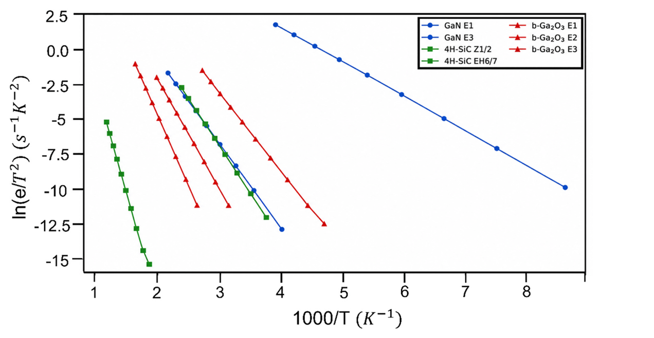
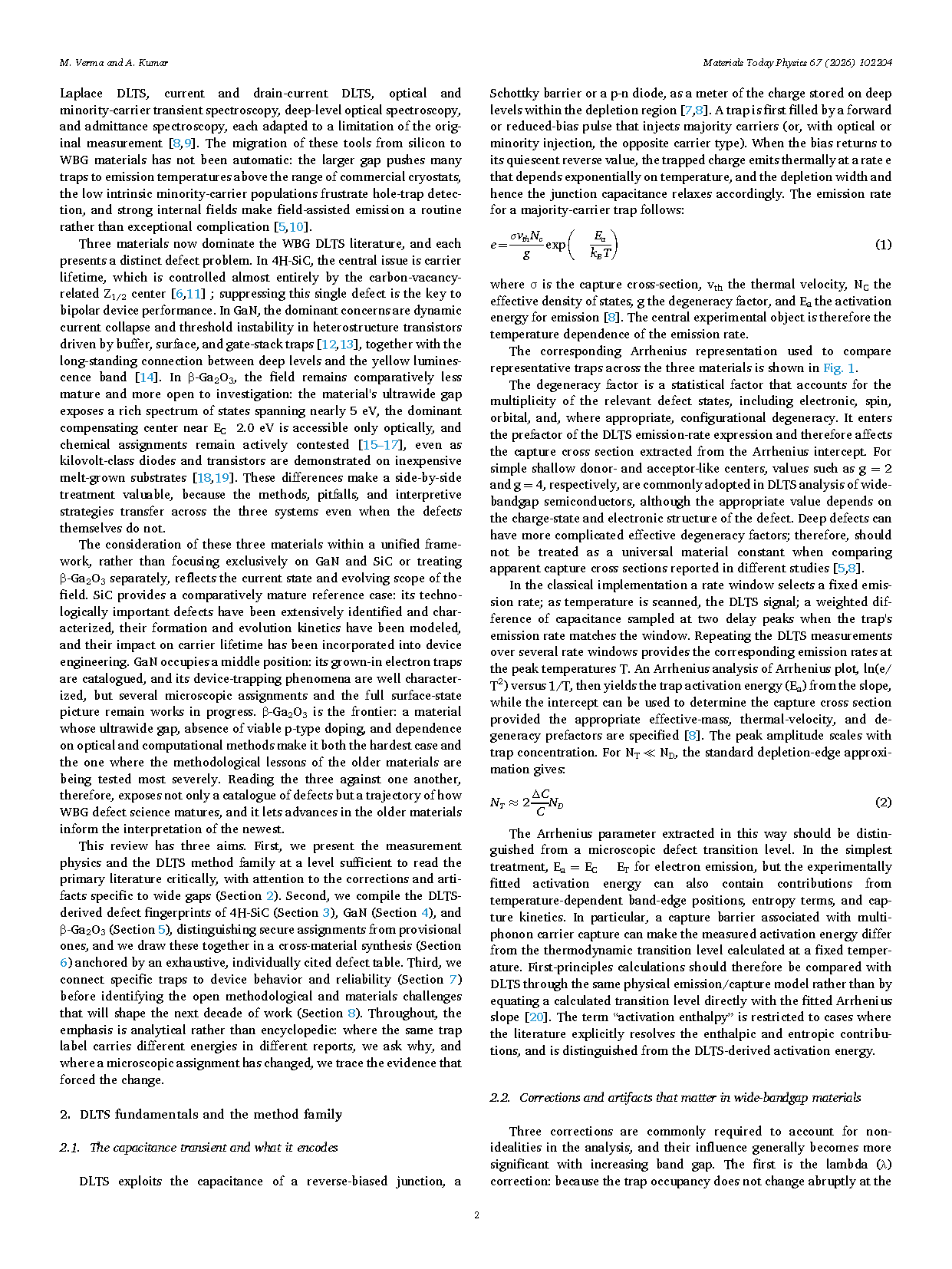
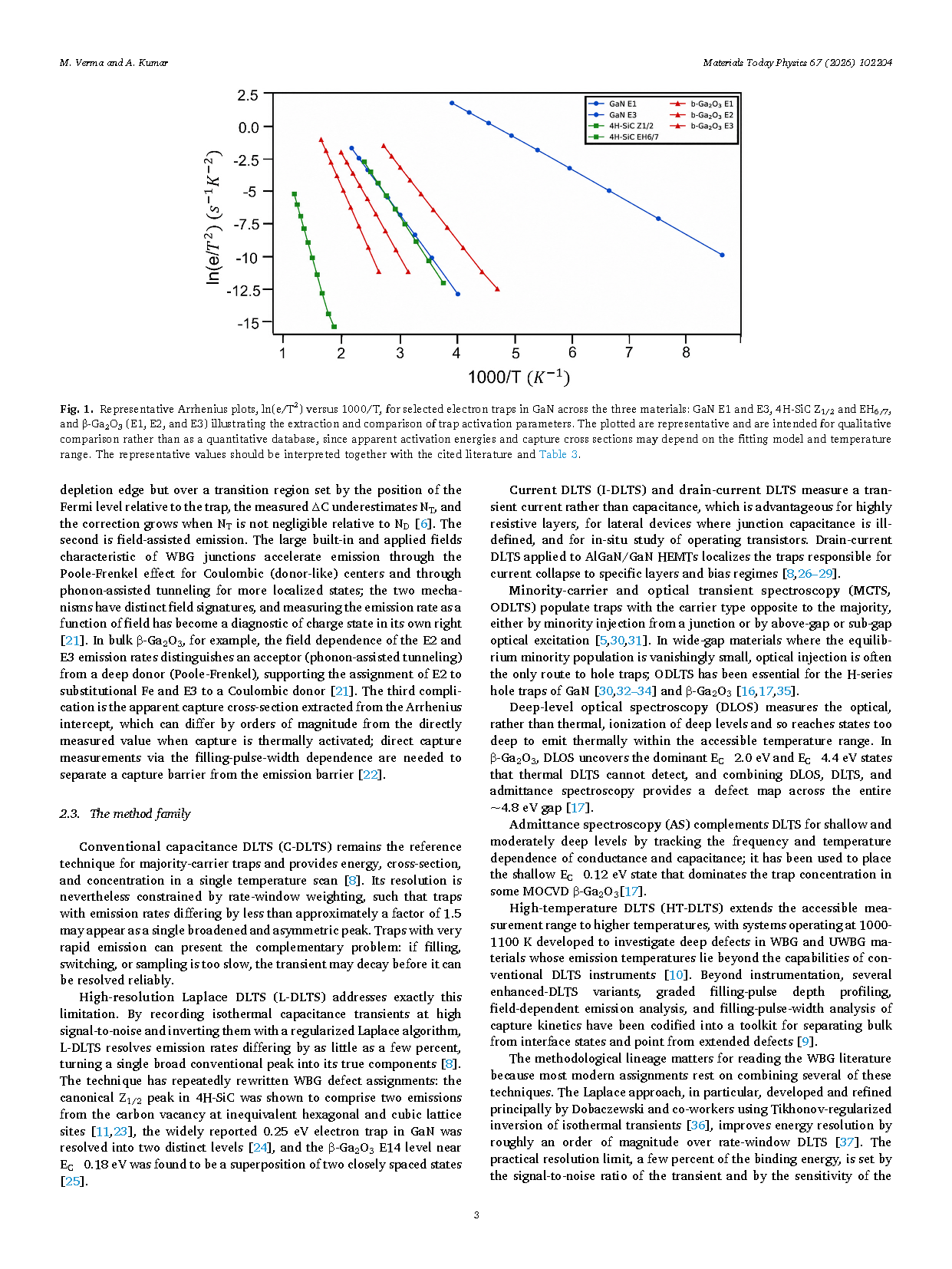
Fig. 1. Representative Arrhenius plots, ln(e/T2) versus 1000/T, for selected electron traps in GaN across the three materials: GaN E1 and E3, 4H-SiC Z1/2 and EH6/7, and β-Ga₂O₃(E1, E2, and E3) illustrating the extraction and comparison of trap activation parameters. The plotted are representative and are intended for qualitative comparison rather than as a quantitative database, since apparent activation energies and capture cross sections may depend on the fitting model and temperature range.
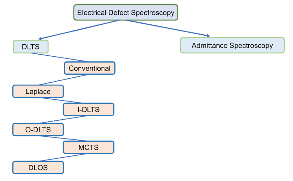
Fig. 2. Schematic of the DLTS method family. A reverse-biased junction is pulsed to fill traps; the thermally activated capacitance (or current) transient on return to reverse bias is analyzed by rate-window correlation (conventional C-DLTS), Laplace inversion (L-DLTS), current detection (I-DLTS/drain-current DLTS), optical or minority injection (ODLTS/MCTS), optical ionization (DLOS), or frequency-domain analysis (admittance spectroscopy). Each branch addresses a specific limitation noted in the text.
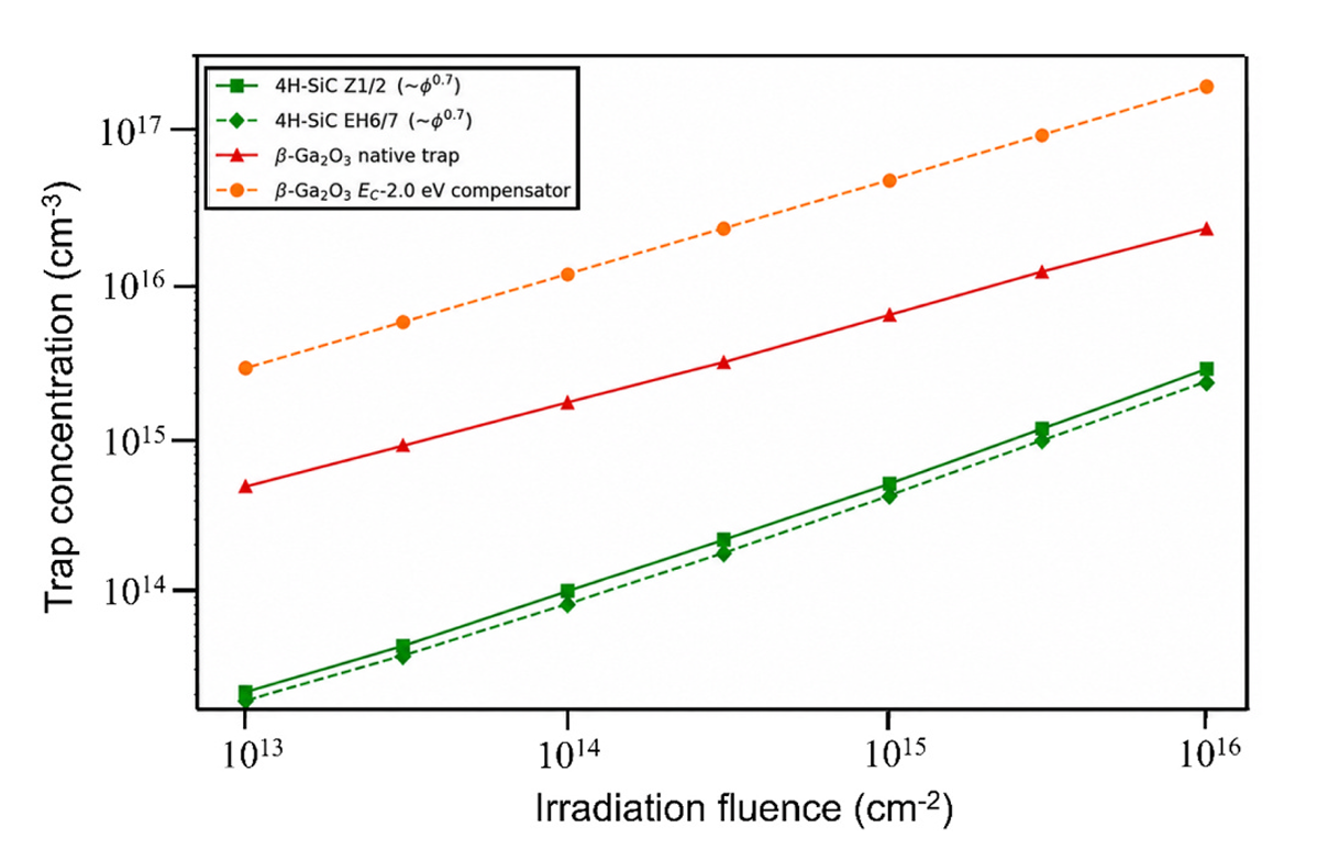
Fig. 3. Representative trap concentration/introduction-rate behavior versus irradiation fluence, illustrating the 0.7-power dependence of Z1/2 and EH6/7 in 4H-SiC and the carrier-removal-driven growth of native-defect-related electron traps and the EC-2.0 eV compensator in β-Ga₂O₃.
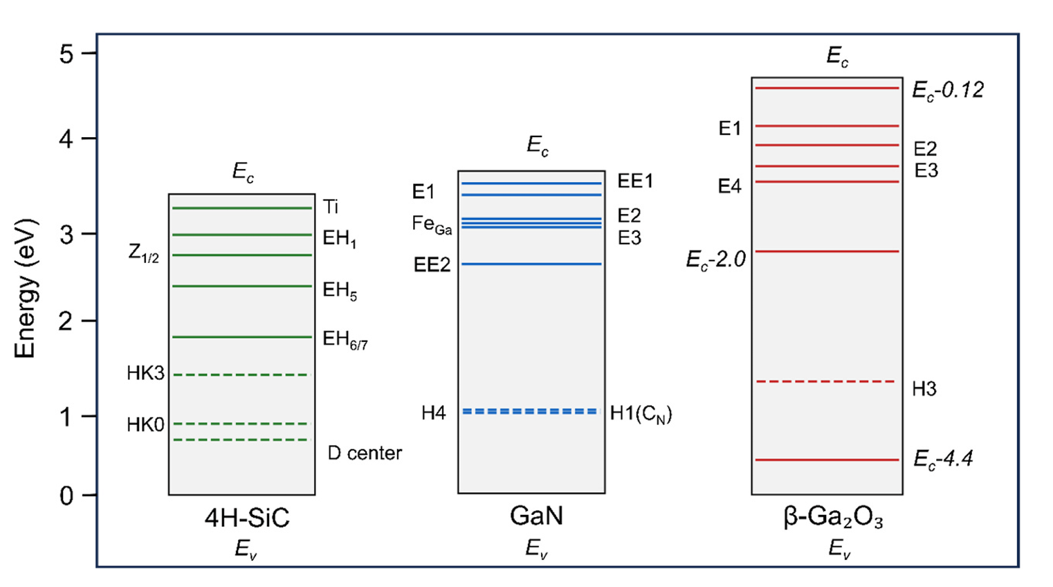
Fig. 4. Defect-fingerprint energy-level map placing the principal DLTS- and DLOS-detected traps of GaN, 4H-SiC, and β-Ga₂O₃ on a common energy axis referenced to each conduction-band minimum (electron traps) and valence-band maximum (hole traps), drawn to the same scale to expose the position of each material's dominant electrically active defect relative to the thermal-DLTS window.
DOI:
doi.org/10.1016/j.mtphys.2026.102204
Instruction
Official Account

Cooperation
Top
