


Researchers from the Ningbo Institute of Materials Technology and Engineering, Chinese Academy of Sciences 、Harbin Institute of Technology and Hangzhou Garen Semiconductor Company Ltd have published a dissertation titled "3 kV-Class β-Ga₂O₃ Lateral MOSFETs With Superior High-Temperature Leakage Suppression Enabled by an Ozone-Grown Semi-Insulating Buffer Layer " in IEEE Transactions on Electron Devices.
Background
With an ultra‑wide bandgap of 4.8 eV, excellent Baliga’s figure of merit, and commercially available melt‑grown bulk substrates, β‑Ga₂O₃ is a promising candidate for next‑generation power electronics outperforming SiC and GaN. In recent years, β‑Ga₂O₃‑based power devices have achieved great progress. Lateral MOSFETs have drawn much attention owing to their good reliability and breakdown performance.
Nevertheless, high‑temperature leakage remains a critical challenge for lateral β‑Ga₂O₃ devices. At 200 °C, the OFF‑state leakage current commonly rises to 10⁻³ ~ 10⁻⁴ mA/mm. Conventional devices adopt Fe‑doped semi‑insulating substrates. Although Fe compensates free electrons at room temperature, compensated electrons get thermally activated at high temperature and produce substrate leakage paths. Moreover, donor‑type traps in unintentionally doped buffer layers and their interfaces bring additional lateral leakage. Previous works adopted Mg‑doped buffer layers or Fe ion‑implanted layers for leakage suppression. However, Mg and Fe dopants tend to diffuse during thermal fabrication processes, leading to degraded interfacial quality and poor device reliability. To address this issue, the team prepared intrinsic semi‑insulating buffer layers by pulsed laser deposition (PLD) under ozone ambient and investigated improvements on high‑temperature and high‑voltage electrical performance.
Abstract
Ultra wide bandgap β-Ga₂O₃ holds great promise for next-generation high-voltage power electronics, yet its practical application is severely hampered by premature breakdown and excessive OFF-state leakage at elevated temperatures. Here, we address the critical challenge by introducing an O₃-assisted-grown semi-insulating buffer layer in lateral β-Ga₂O₃ MOSFETs. The buffer layer exhibits a high density of deep-level acceptor defects, specifically gallium vacancies and gallium-oxygen divacancy complexes, as revealed by photoluminescence spectroscopy, which effectively compensate thermally activated carriers and suppress leakage pathways. Devices incorporating this buffer layer achieve a record breakdown voltage exceeding 3 kV among pulsed laser deposition (PLD)-grown lateral β-Ga₂O₃ MOSFETs without a field plate, and a specific on-resistance of 206.84 mΩ·cm². Moreover, at an operating temperature of 200 °C, the OFF-state leakage current is reduced by nearly two orders of magnitude compared to devices without the buffer layer. Temperature-dependent current-voltage measurements and TCAD simulations reveal that the superior high-temperature insulation originates from the deep level defects (2.4–3.1 eV) in the O₃-grown buffer layer, which contrasts with the shallower Fe-related acceptor level (~0.8 eV) in conventional substrates. This work demonstrates that defect-engineered buffer layers offer a viable and scalable pathway to exceptional high-temperature stability in β-Ga₂O₃ lateral power devices.
Highlights
The team adopted PLD to grow semi‑insulating β‑Ga₂O₃ buffer layer under ozone ambient. High‑density deep‑level acceptor defects including gallium vacancies and gallium‑oxygen divacancy complexes are introduced without extrinsic doping or ion implantation, avoiding performance degradation induced by dopant diffusion under high‑temperature process.
Compared with devices without buffer layer, the MOSFET equipped with ozone‑grown buffer layer achieves nearly two‑orders‑of‑magnitude lower drain leakage at 200 °C, accompanied by suppressed gate leakage and improved high‑temperature OFF‑state performance.
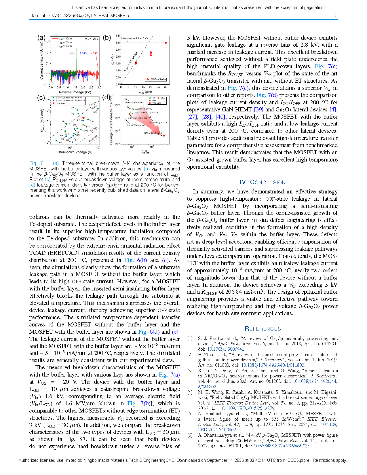
Without field‑plate or other edge‑termination structures, the device with LGD=30 μm achieves breakdown voltage over 3 kV and specific ON‑resistance of 206.84 mΩ⋅cm 2, delivering competitive comprehensive power‑device performance.
Combining PL characterization and drift-diffusion TCAD simulation, the mechanism is illustrated. Shallow Fe-related acceptor level (~0.8 eV) triggers thermally-activated leakage at high temperature, while deep-level intrinsic defects (2.4–3.1 eV) inside buffer layer trap thermally-excited carriers and block substrate-mediated leakage paths.
The team verified epitaxial engineering of intrinsic-defect buffer layer as a feasible and effective technical route for high-voltage β-Ga₂O₃ power devices operating under harsh high-temperature conditions.
Conclusion
In summary, we have demonstrated an effective strategy to suppress high-temperature OFF-state leakage in lateral β-Ga₂O₃ MOSFET by incorporating a semi-insulating β-Ga₂O₃ buffer layer. Through the ozone-assisted growth of the β-Ga₂O₃ buffer layer, in situ defect engineering is effectively realized, resulting in the formation of a high density of VGa and VGa-VO within the buffer layer. These defects act as deep-level acceptors, enabling efficient compensation of thermally activated carriers and suppressing leakage pathways under elevated temperature operation. Consequently, the MOSFET with the buffer layer exhibits an ultralow leakage current of approximately 10⁻⁶ mA/mm at 200 °C, nearly two orders of magnitude lower than that of the device without a buffer layer. In addition, the device achieves a Vbr exceeding 3 kV and a RON,SP of 206.84 mΩ·cm². The design of epitaxial buffer engineering provides a viable and effective pathway toward realizing high-temperature and high-voltage β-Ga₂O₃ power devices for harsh-environment applications.
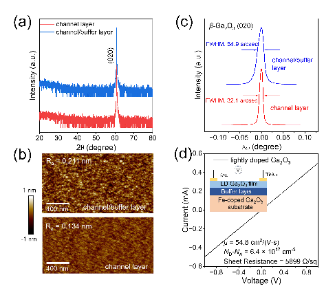
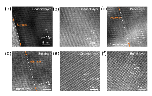
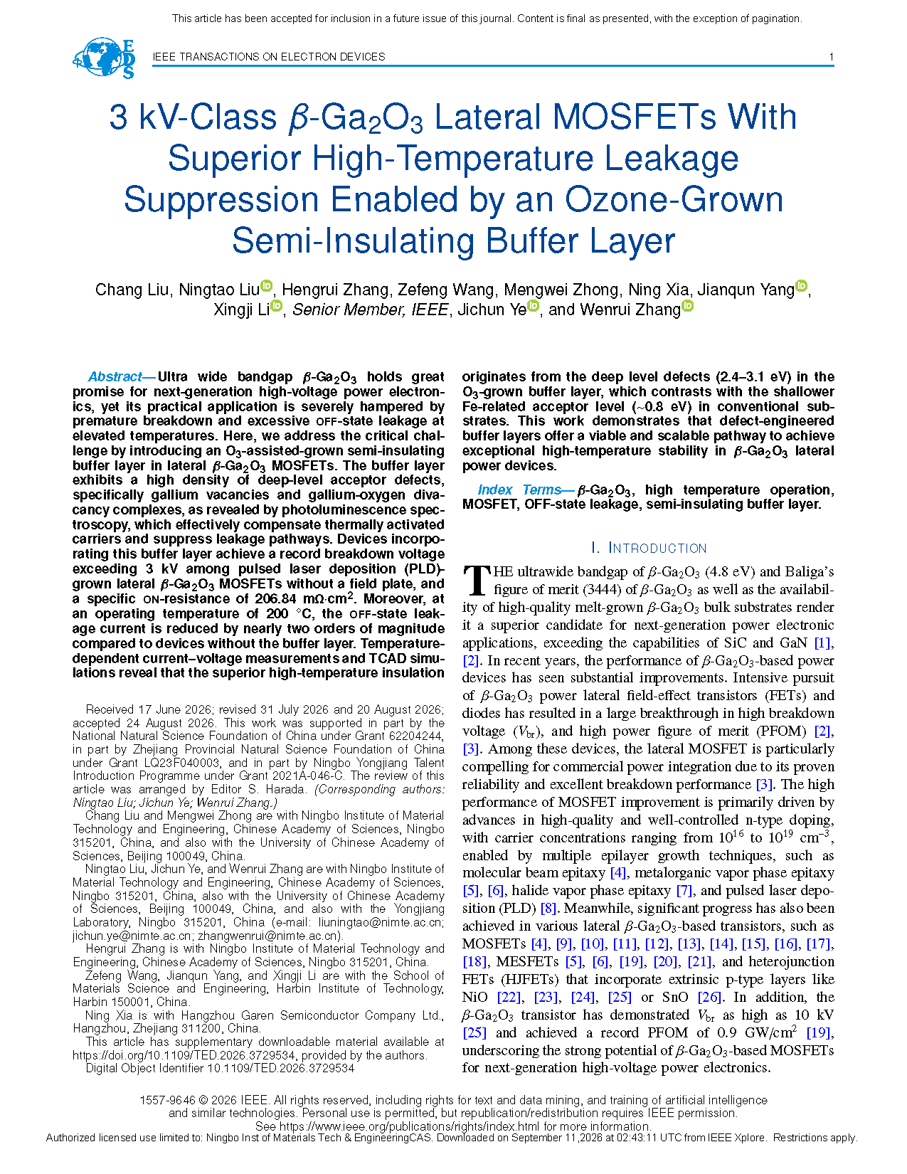
Fig. 1. (a) θ-2θ XRD full scans and (b) RC profiles of the single channel layer and the double channel/buffer layer grown on the (010) Fe-doped β-Ga₂O₃ substrate. (c) AFM images of the β-Ga₂O₃ films showing a smooth surface morphology. (d) I-V characteristics of Ti/Au contacts on the β-Ga₂O₃ film. The inset shows the measurement structure, and the extracted carrier concentration, mobility, and sheet resistance from Hall measurement are listed.
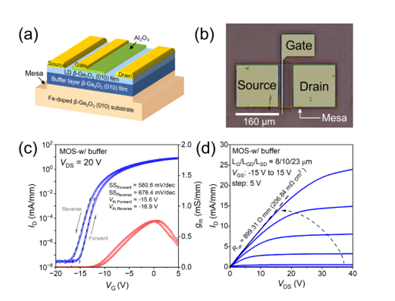
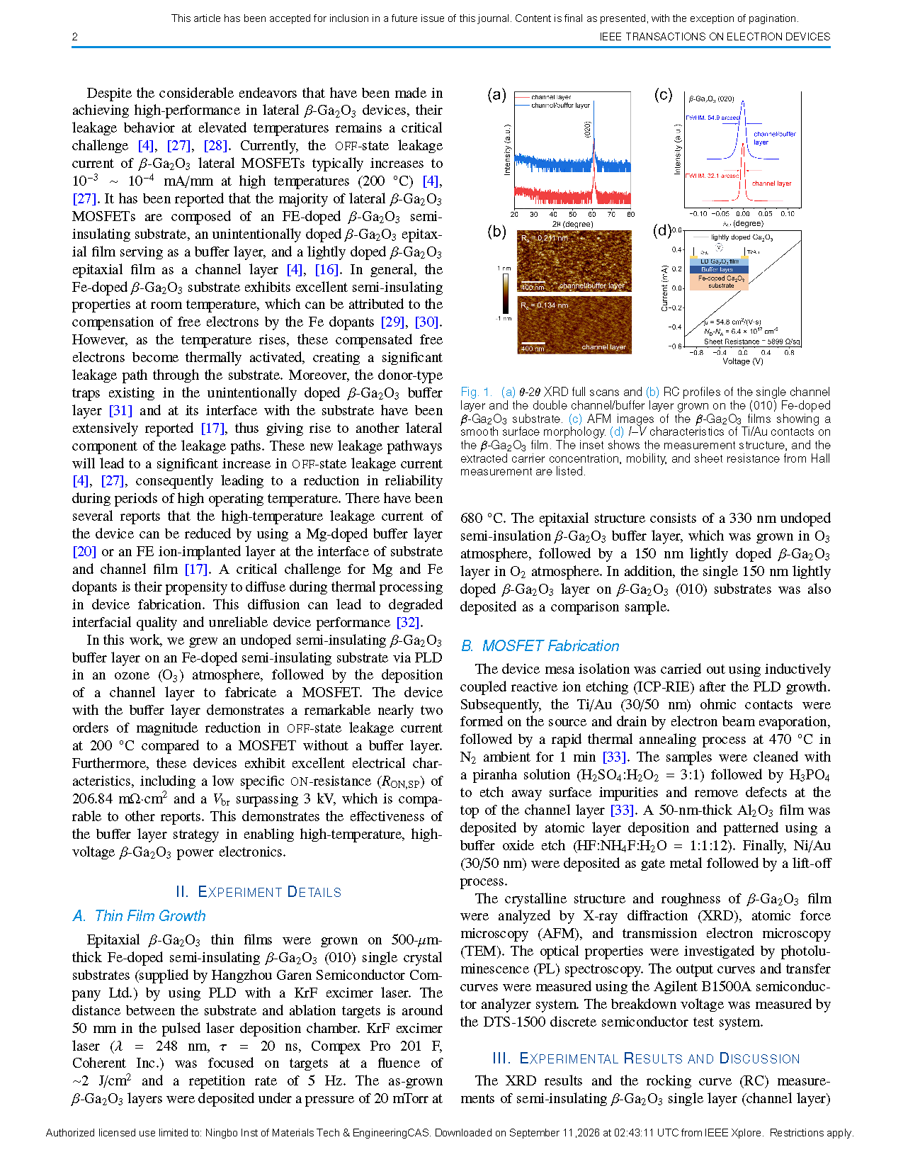
Fig. 2. HRTEM images of the β-Ga₂O₃ (010) film projected along the [201] zone axis, including the β-Ga₂O₃ (a) top surface area, (b) channel layer, (c) interface of channel layer and buffer layer, and (d) interface of buffer layer and substrate. (e) and (f) Magnified views of the channel and buffer layers, respectively.
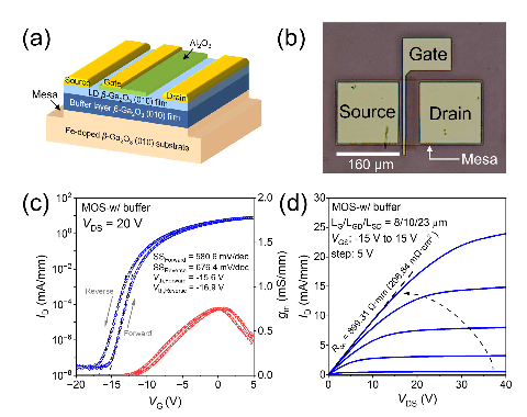
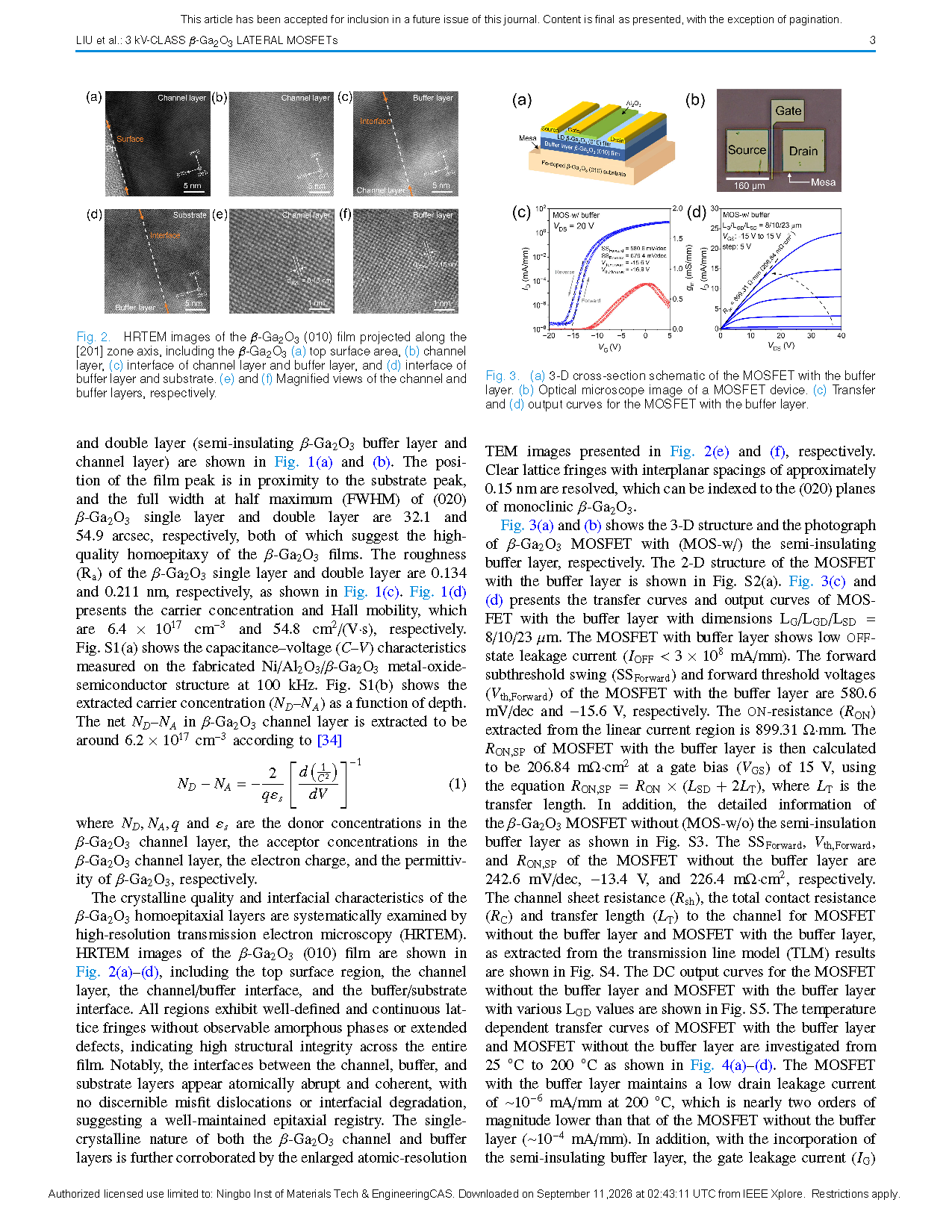
Fig. 3. (a) 3-D cross-section schematic of the MOSFET with the buffer layer. (b) Optical microscope image of a MOSFET device. (c) Transfer and (d) output curves for the MOSFET with the buffer layer.
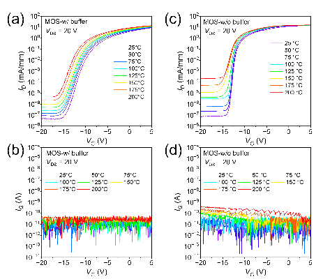
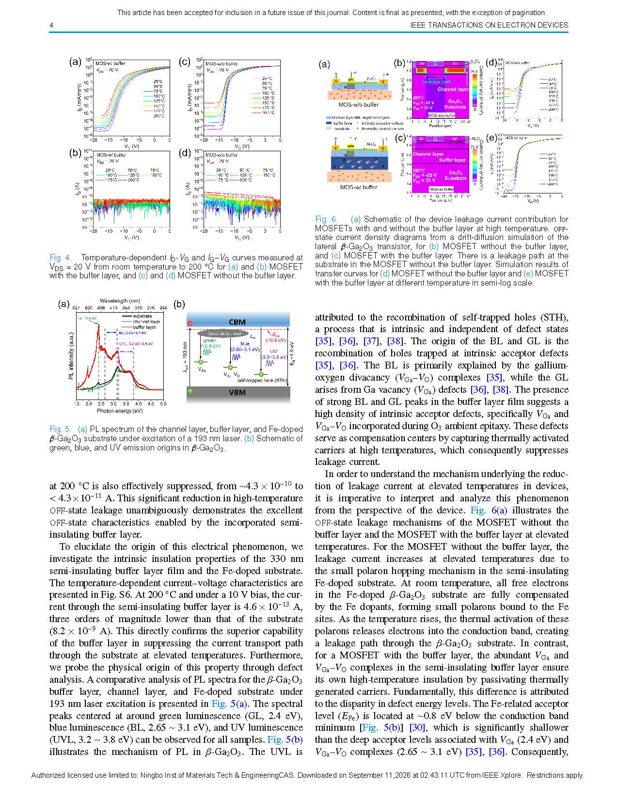
Fig. 4. Temperature-dependent ID-VG and IG-VG curves measured at VDS = 20 V from room temperature to 200 °C for (a) and (b) MOSFET with the buffer layer, and (c) and (d) MOSFET without the buffer layer.
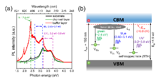
Fig. 5. (a) PL spectrum of the channel layer, buffer layer, and Fe-doped β-Ga₂O₃ substrate under excitation of a 193 nm laser. (b) Schematic of green, blue, and UV emission origins in β-Ga₂O3.
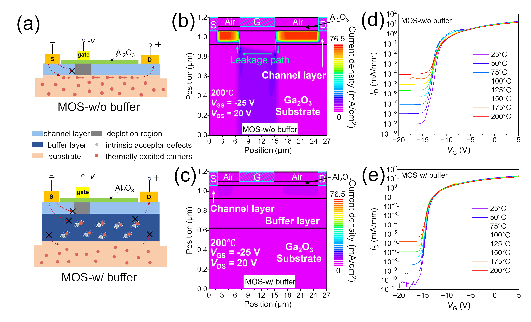
Fig. 6. (a) Schematic of the device leakage current contribution for MOSFETs with and without the buffer layer at high temperature. OFF-state current density diagrams from a drift-diffusion simulation of the lateral β-Ga₂O₃ transistor, for (b) MOSFET without the buffer layer, and (c) MOSFET with the buffer layer. There is a leakage path at the substrate in the MOSFET without the buffer layer. Simulation results of transfer curves for (d) MOSFET without the buffer layer and (e) MOSFET with the buffer layer at different temperature in semi-log scale.
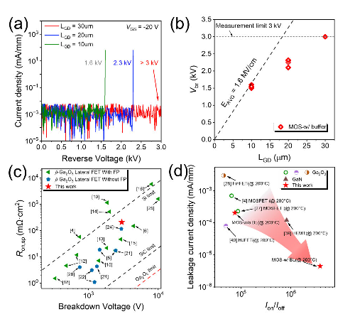
Fig. 7. (a) Three-terminal breakdown I-V characteristics of the MOSFET with the buffer layer with various LGD values. (b) Vbr measured in the β-Ga₂O₃ MOSFET with the buffer layer as a function of LGD. Plot of (c) RON,SP versus breakdown voltage at room temperature and (d) leakage current density versus ION/IOFF ratio at 200 °C for benchmarking this work with other recently published data on lateral β-Ga₂O₃ power transistor devices.
DOI:
10.1109/TED.2026.3729534
Instruction
Official Account

Cooperation
Top
