


Recently, the "2026 AI Innovation Applications Top 50" Exemplary Cases List was officially unveiled. Centered on the theme "New Paradigms for AI Collaboration in the 15th Five-Year Plan", the organizing committee assembled experts from industry, scientific research and capital sectors. Through multiple rounds of rigorous screening including preliminary document review, joint expert review, real-world implementation verification and comprehensive deliberation, it conducted holistic evaluation from dimensions of technological innovation, implementation effectiveness, industrial contribution and social value, and finally selected 50 benchmark enterprises and exemplary cases. Hangzhou Garen Semiconductor Co., Ltd. (hereinafter referred to as "Garen Semiconductor") made the list with its case "Multi-Agent Collaboration for Casting-Based Crystal Growth", alongside leading enterprises from diverse fields such as Huawei and CRRC.
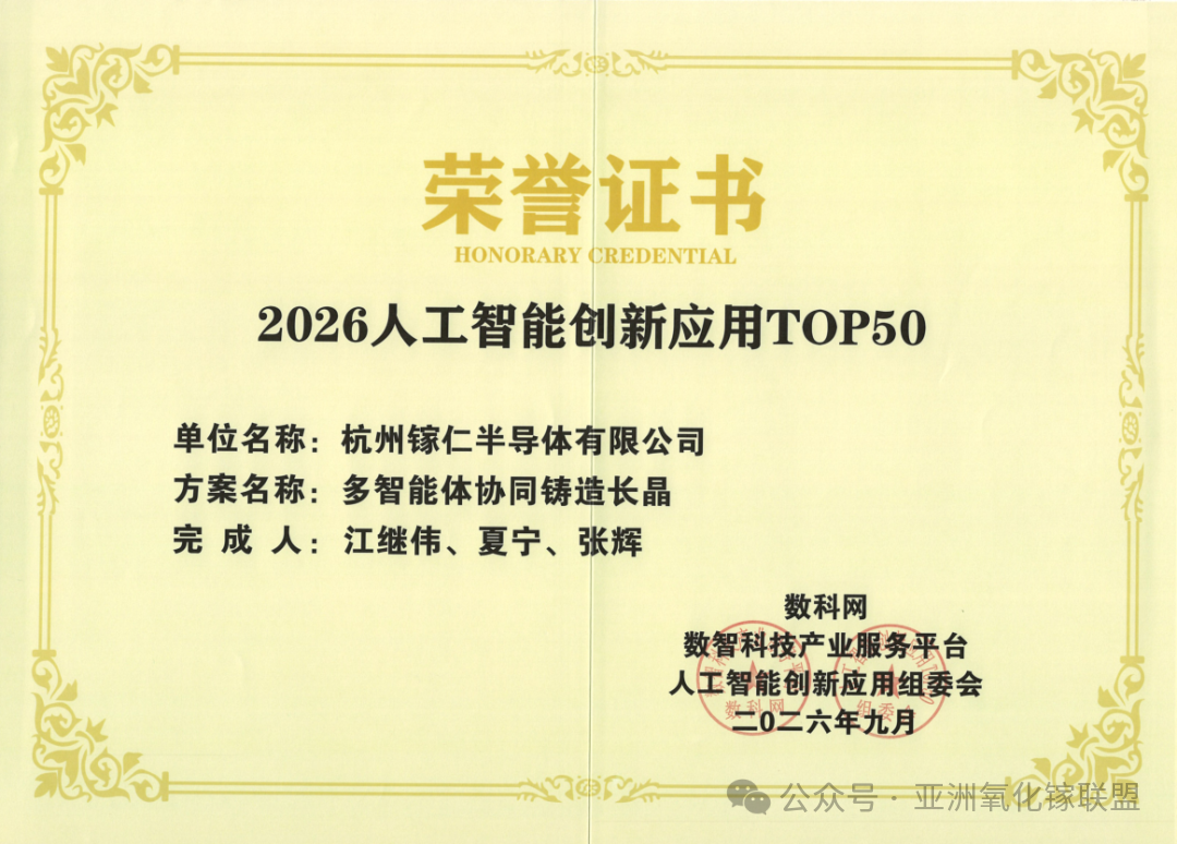
Figure 1 Award Certificate of Garen Semiconductor
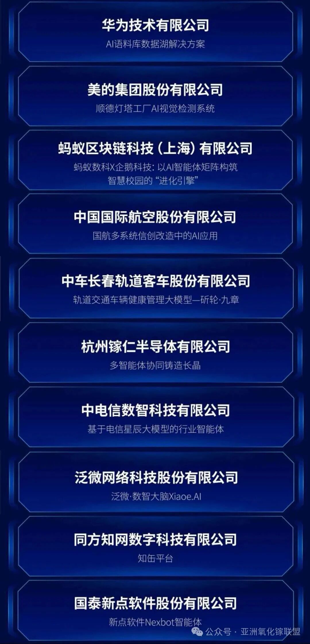
Figure 2 Excerpt from the 2026 AI Innovation Applications Top 50 Exemplary Cases List
Core to this award is Garen Semiconductor’s exploration into the deep integration of AI technologies with its self-developed casting-based crystal-growth process. Crystal growth is an extremely complex procedure, where factors including furnace temperature and melt status are interrelated. For a long time, process tuning has largely depended on engineers’ experiential know-how. By adopting multi-agent AI collaboration technology, the monitoring, analysis and regulation of crystal-growth procedures have become more convenient and precise, delivering solid technical support for the transition of casting-method gallium oxide single crystals from laboratory R&D to large-scale production.
This honor recognizes Garen Semiconductor’s innovative "Crystal-Growth Technology + AI" development path, stemming from the team’s years-long in-depth engagement in gallium oxide crystal growth. Starting from 2-inch up to 8-inch gallium oxide single-crystal substrates, followed by the completion and commissioning of a mass-production homoepitaxial production line compatible with 6-inch and 8-inch wafers, Garen Semiconductor has achieved continuous breakthroughs in core key technologies for fourth-generation semiconductors, accelerating the industrialization of gallium-oxide materials.
Going forward, Garen Semiconductor will keep delving into ultra-wide-bandgap semiconductor materials, fully tap the application potential of AI technologies in crystal-growth processes, and contribute Garen-level strength to the development of China’s fourth-generation semiconductor industry.
About Garen Semiconductor
Hangzhou Garen Semiconductor Co., Ltd. is a world-leading provider of gallium-oxide material and equipment solutions, focusing on R&D and industrial implementation for ultra-wide-bandgap semiconductors. Its core products cover: 2-inch to 12-inch gallium-oxide single crystals and substrates (world’s first constant-diameter growth for 8-inch and 12-inch specifications), gallium-oxide crystal-growth equipment adopting the Vertical Bridgman (VB) method, as well as 2-inch to 8-inch gallium-oxide homoepitaxial wafers (the 8-inch version is a world premiere). The company is committed to building a full-chain product ecosystem of "Equipment-Crystal-Substrate-Epitaxy" and delivering systematic solutions for customers worldwide. Its achievements in gallium-oxide technologies have been covered in special reports by authoritative media outlets including People’s Daily, Xinhua News Agency, Science and Technology Daily, Sina Finance, China Blue News and The Paper.
For more information, please visit the official website: http://garen.cc/
Or contact us:
Mr. Jiang
Phone: +86 159 1871 9807
Email: jiangjiwei@garen.cc
Mr. Xia
Phone: +86 190 1127 8792
Email: xianing@garen.cc
Instruction
Official Account

Cooperation
Top
