


Prof. Xinke Liu's team at Shenzhen University has published an article entitled “2-kV Vertical β-Ga2O3 MOSFET With p-Cu2O Body via Barrier Modulated Electron Transport” in IEEE Electron Device Letters.
Background
β-Ga2O3 has an ultra-wide bandgap of approximately 4.8 eV and a theoretical critical electric field of 8 MV/cm. Its Baliga figure of merit is significantly higher than those of SiC and GaN, making it an important candidate material for next-generation high-voltage power electronic devices. For high-voltage applications, vertical MOSFETs can increase the breakdown voltage by increasing the drift-layer thickness without significantly increasing the chip area, making them an important device architecture for fully exploiting the high critical electric field of β-Ga2O3. However, stable and effective p-type doping has long been unavailable in β-Ga2O3, making it difficult to directly implement the p-body structure used in conventional power MOSFETs. Existing approaches such as FinFETs and current-blocking-layer (CBL) structures can realize normally-off devices, but they face complicated fabrication processes or a trade-off between conduction and blocking performance. NiO is a widely used p-type oxide; however, its conduction band is dominated by localized Ni 3d states, which are associated with a large electron effective mass and strong electron scattering. In contrast, Cu2O features more delocalized Cu 4s-derived conduction-band states and a smaller conduction-band offset with β-Ga2O3, facilitating electron injection and transport across the heterojunction. Therefore, p-Cu2O was employed as the p-body layer to construct an all-oxide n+-ZnO/p-Cu2O/n-Ga2O3 vertical trench MOSFET.
Abstract
The team fabricated a vertical enhancement-mode trench MOSFET based on an n+-ZnO/p-Cu2O/n-Ga2O3 heterojunction. The device employs a 200 nm n+-ZnO source layer, a 300 nm p-Cu2O body region, and a 10 μm n--Ga2O3 drift layer, with carrier concentrations of 1.41×10¹⁹, 1.03×10¹⁷, and 8.01×1015 cm-3 respectively, together with a 50 nm Al2O3 gate dielectric. TEM and EDS characterization reveal smooth interfaces and uniform elemental distributions across the functional layers, while XRD and XPS further verify the crystalline quality and chemical compositions of ZnO, Cu2O, and β-Ga2O3. The p-Cu2O/n+-ZnO heterojunction exhibits a rectification ratio above 106, while the p-Cu2O/n--Ga2O3 heterojunction achieves an Ion/Ioff ratio of 108 with low reverse leakage. The fabricated MOSFET remains off at VGS=0 V, with a threshold voltage Vth=7 V, a double-sweep threshold shift of only 0.21 V, an Ion/Ioff ratio of approximately 106, and a specific on-resistance Ron,sp=2.93 Ω·cm2. The C-V characteristics show only accumulation and depletion, with no conventional inversion layer observed. A positive gate bias pulls down the energy bands of the fully depleted p-Cu2O layer, reducing the electron-injection barrier at the n+-ZnO/p-Cu2O heterojunction, while the drain bias further establishes continuous source-to-drain transport. Temperature-dependent transfer characteristics and Arrhenius analysis demonstrate that the process is dominated by thermionic emission, and the extracted effective barrier height continuously decreases with increasing VGS. The device ultimately achieves a maximum breakdown voltage of 2000 V.
Highlights
①p-Cu2O is employed as the heterojunction p-type body of the vertical β-Ga2O3 MOSFET, forming an all-oxide n+-ZnO/p-Cu2O/n-Ga2O3 n-p-n structure and providing a new device route to circumvent the lack of effective p-type doping in β-Ga2O3.
②A gate-controlled barrier-modulated electron transport mechanism is proposed and experimentally verified. Rather than relying on a minority-carrier inversion channel in a conventional p-body, device switching is controlled by gate modulation of the heterojunction electron-injection barrier.
③The device achieves Vth=7 V, Ion/Ioff≈106, BV=2000 V, and Ron,sp=2.93 Ω·cm2, combining enhancement-mode operation with 2-kV high-voltage blocking capability.
Conclusion
This work employs p-Cu2O as a heterojunction p-type body to successfully realize a vertical enhancement-mode trench MOSFET based on an all-oxide n+-ZnO/p-Cu2O/n-Ga2O3 heterojunction, overcoming the limitation imposed by the lack of stable p-type doping in β-Ga2O3 on conventional p-body structures. Device conduction does not rely on an inversion layer; instead, electron injection is controlled through gate modulation of the heterojunction barrier. Temperature-dependent measurements, Arrhenius fitting, and effective barrier-height extraction collectively verify this transport mechanism. The device achieves a threshold voltage of 7 V, an on/off ratio of approximately 106, a maximum breakdown voltage of 2000 V, and a specific on-resistance of 2.93 Ω·cm2. The heterojunction p-body structure and barrier-modulation mechanism provide a new design strategy for high-performance vertical β-Ga2O3 power MOSFETs.
Project Support
This work was supported in part by the National Key Research and Development Program of China under Grant 2024YFE0205100, in part by Guangdong Major Project of Basic and Applied Basic Research under Grant 2023B0303000012, in part by Shenzhen Science and Technology Program under Grant SGDX20240115101802004, in part by the State Key Laboratory of Radio Frequency Heterogeneous Integration Independent Scientific Research Program under Grant 2025007, and in part by the Scientific Instrument Developing Project of Shenzhen University under Grant 2024YQ003.
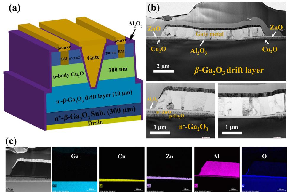
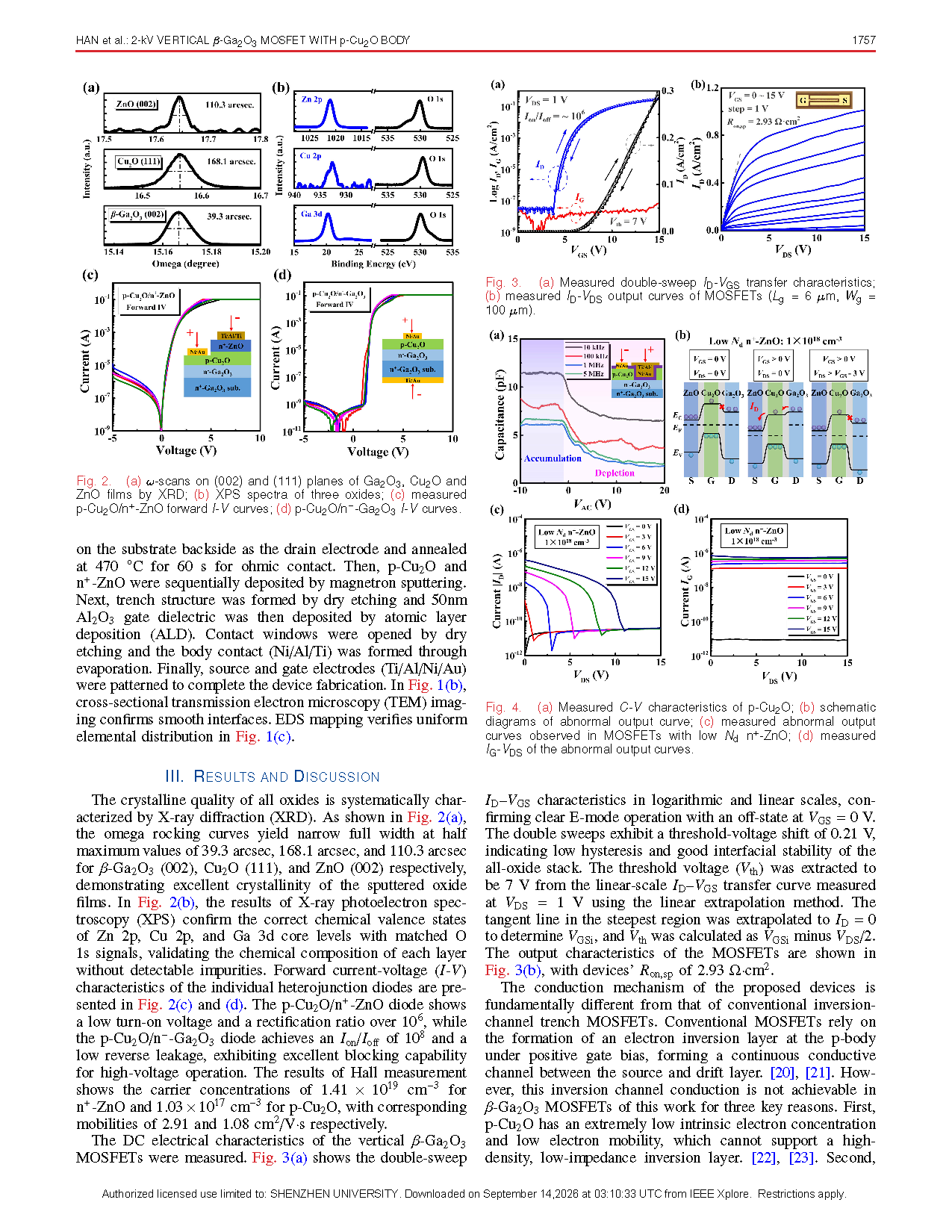
Figure 1. (a) Schematic structure of the vertical β-Ga2O3 trench MOSFET; (b) TEM observation region of the device cross section; (c) EDS elemental mapping of the functional layers.
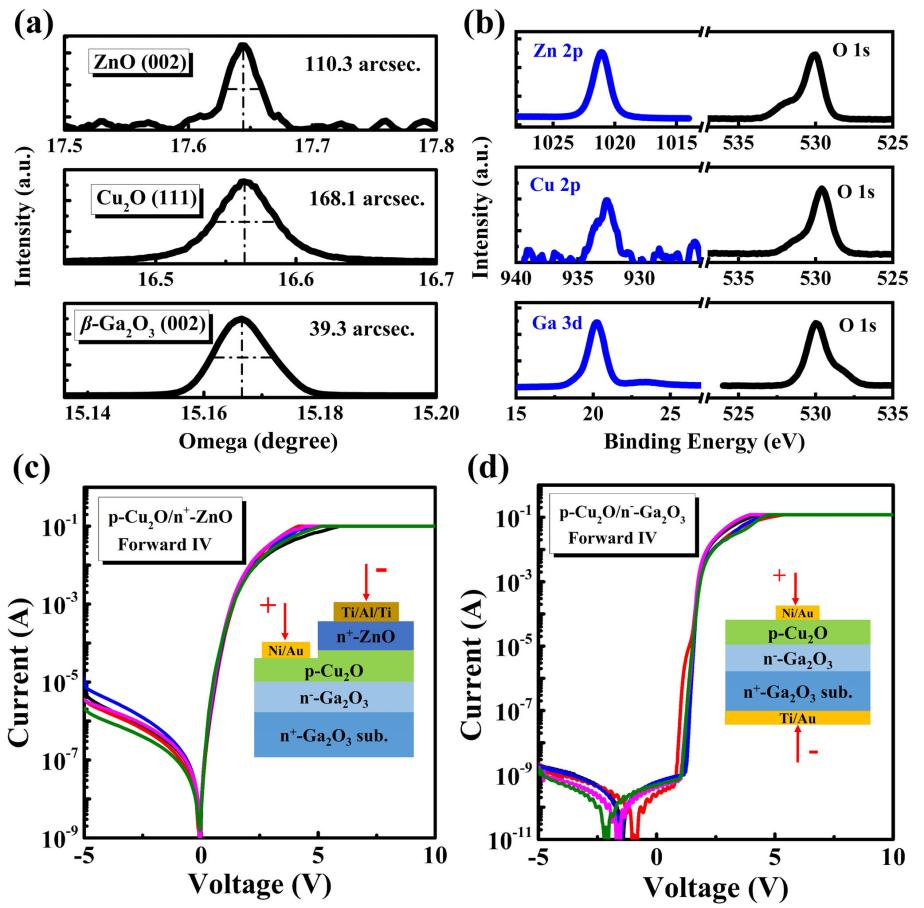
Figure 2. (a) XRD ω-rocking curves of β-Ga2O3, Cu2O, and ZnO films; (b) XPS spectra of the three oxides; (c) forward I-V characteristics of the p-Cu2O/n+-ZnO heterojunction; (d) I-V characteristics of the p-Cu2O/n--Ga2O3 heterojunction.
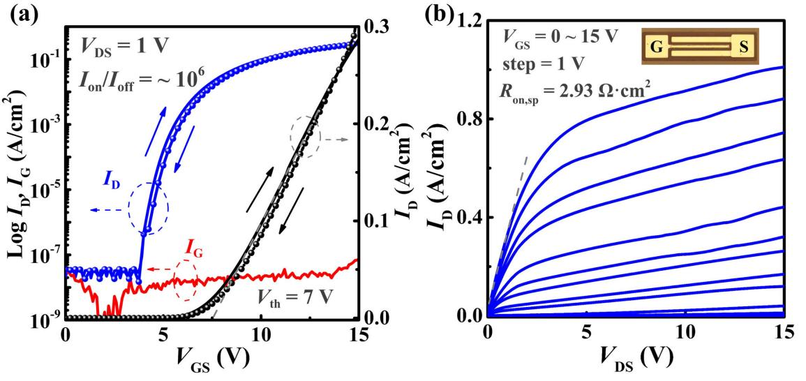
Figure 3. (a) Double-sweep ID-VGS transfer characteristics of the MOSFET; (b) ID-VGS output characteristics (Lg=6 μm, Wg=100 μm).
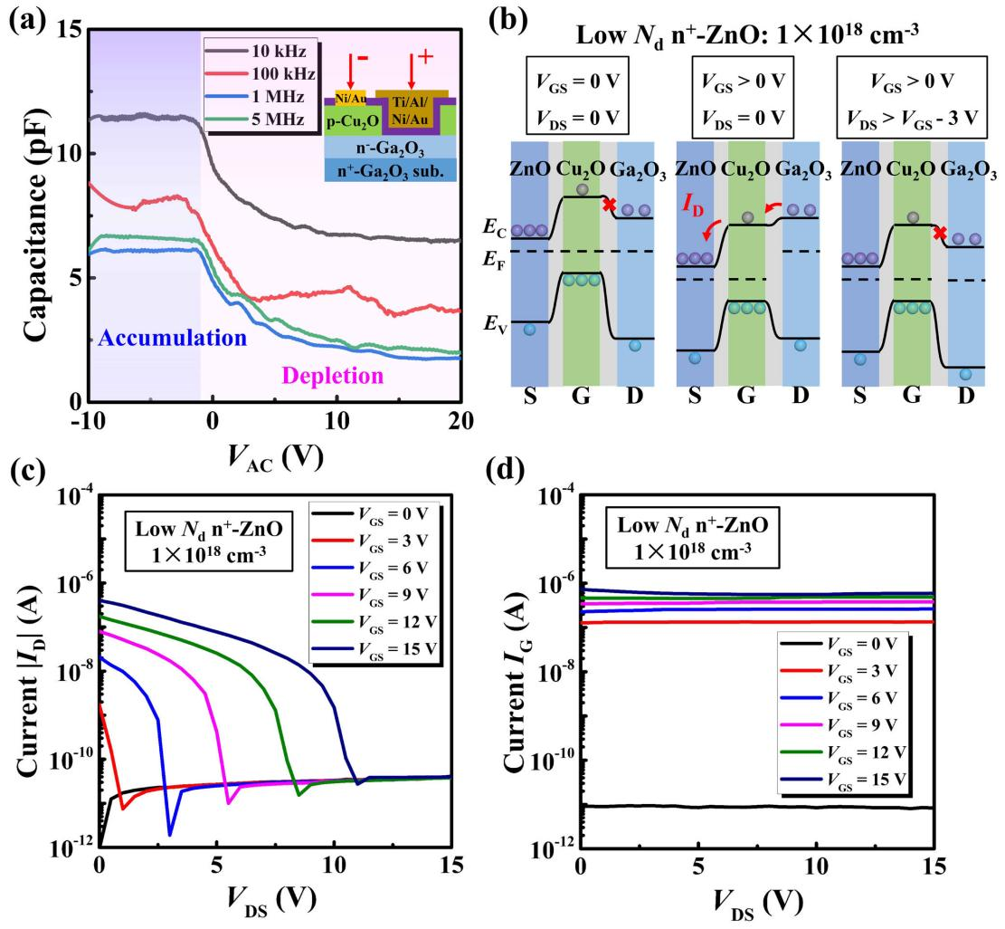
Figure 4. (a) C-V characteristics of p-Cu2O; (b) band diagram illustrating the abnormal output characteristics; (c) abnormal output curves of devices with low-carrier-concentration n+-ZnO; (d) corresponding IG-VDS characteristics.
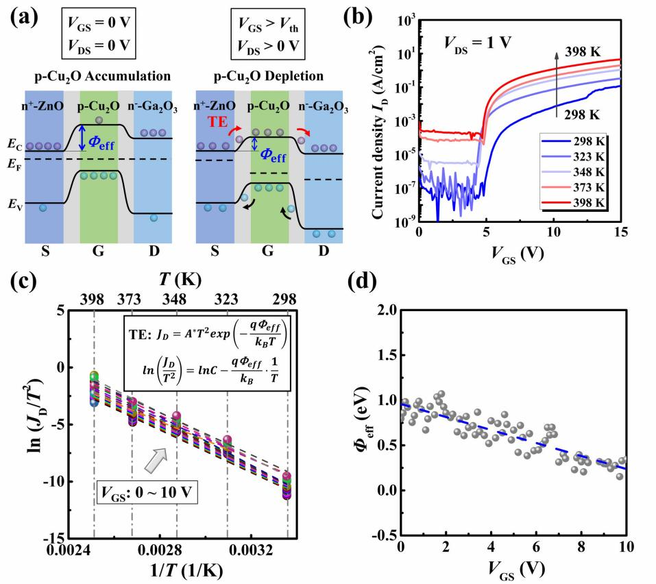
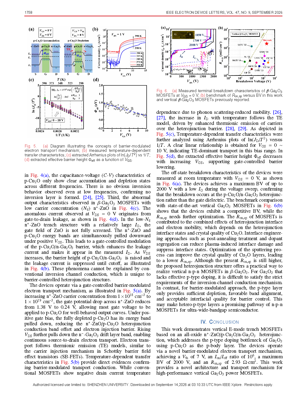
Figure 5. (a) Schematic illustration of the gate-controlled barrier-modulated electron transport mechanism; (b) temperature-dependent transfer characteristics; (c) Arrhenius plots of ln(JD/T2) versus 1/T; (d) extracted effective barrier height Φeff as a function of VGS.
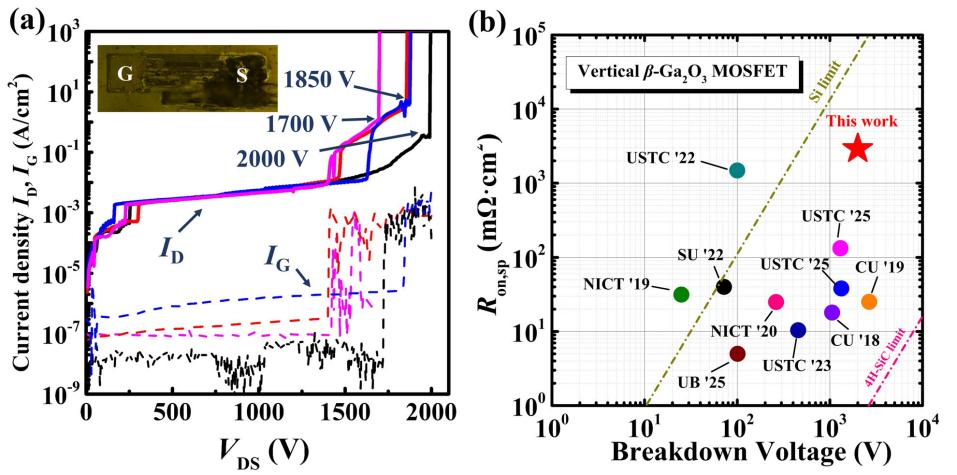
Figure 6. (a) Terminal breakdown characteristics of the device at VGS=0 V; (b) Ron,sp-BV benchmark comparison between this work and previously reported vertical β-Ga2O3 MOSFETs.
Introduction of corresponding author
Xinke Liu is a National Young Talent (2025), Chief Scientist of a National Key Research and Development Program of the Ministry of Science and Technology of China (2025), Fellow of the Institute of Physics (FInstP, 2025), Fellow of the Royal Society of Chemistry (FRSC, 2024), and Ph.D. supervisor. He received his Honors Bachelor's degree in Materials Science from the National University of Singapore (2008), Ph.D. in Microelectronics from the Department of Electrical and Computer Engineering at the National University of Singapore (2013), and a certification in Technology Management from the National University of Singapore in 2010. He serves as Director of the Institute of Power Semiconductor Devices and AI Energy Monitoring Engineering Technology at Shenzhen University and as a Distinguished Professor in the College of Materials Science and Engineering and the State Key Laboratory of Radio Frequency Heterogeneous Integration. His research has long focused on wide-bandgap semiconductor GaN materials and devices. As first or corresponding author, he has published 131 SCI-indexed papers in international journals including Materials Today, Advanced Materials, IEEE EDL/TED, and others, and has published the books Gallium Nitride Single-Crystal Materials and Devices and Scientific and Technological Archaeology and Cultural Relic Appreciation. He has led major research projects funded by the National Key Research and Development Program of China, National Natural Science Foundation of China projects (Young Scientists Fund and General Program), and the Distinguished Young Scholars Program of the Guangdong Natural Science Foundation. As first awardee or individual recipient, he has received the Bronze Award in the 2021 Guangdong University Science and Technology Achievement Transformation Finals, the 2022 Guangdong Provincial Science and Technology Progress Second Prize, the 2022 Chinese Institute of Electronics Science and Technology Progress Second Prize, the 2022 Guangdong Electronics Society Science and Technology Progress Second Prize, the 2023 Shenzhen Youth Science and Technology Award, and the 2025 Guangdong Youth Science and Technology Award.
DOI:
10.1109/LED.2026.3707936
Instruction
Official Account

Cooperation
Top
