


Researchers from the Hanyang University, Seoul National University, Konkuk University, Samsung Electronics of Korea have published a dissertation titled "Thermally robust HZO/poly-Si ferroelectric stacks enabled by an ultrathin Ga₂O₃ interlayer" in Journal of Alloys and Compounds.
Background
Charge-trap flash (CTF) NAND memory has become the cornerstone of mainstream 3D NAND flash technology. While vertical stacking increases storage density, fundamental physical limitations become pronounced with more stacked layers, including cell-to-cell interference, lateral charge migration, degraded data retention, and reliability degradation. Repeated program/erase cycles generate interface and bulk traps and narrow the memory window, pushing CTF scaling toward its performance limit. Hafnium-oxide-based ferroelectric field-effect transistor (FeFET) memory emerges as a promising successor. Hf₀.₅Zr₀.₅O₂(HZO) features good CMOS compatibility and robust ferroelectricity in ultrathin films, which is critical for high-aspect-ratio vertical integration for 3D NAND. Nevertheless, integrating HZO into 3D NAND encounters severe thermal-budget challenges from the punch-and-plug process. Poly-Si channel crystallization and dopant activation require high-temperature treatments up to 650-900℃. Under high thermal load, the HZO/poly-Si interface is thermodynamically unstable, triggering inter-diffusion, parasitic low-k SiOx formation, depolarization field, voltage drop, metallic defects and electric-field screening, which degrade or eliminate ferroelectric switching. Various interfacial-engineering approaches have been reported previously. The team adopts an ~1nm amorphous Ga2O3 interlayer and investigates its interface-protection performance.
Abstract
Hafnium oxide-based ferroelectrics have emerged as promising candidates for next-generation 3D NAND flash memory, addressing the scaling limitations and retention issues of conventional charge-trap technology. However, integrating these materials with polycrystalline silicon channels is challenged by the thermal budget associated with poly-Si channel crystallization with punch-and-plug process steps in 3D NAND process flows. Such elevated temperatures promote the growth of a parasitic low-permittivity SiOₓ layer and generate metallic defects at the interface, leading to severe electric field screening and ferroelectric degradation. In this work, we demonstrate a thermally stable TiN/Hf₀.₅Zr₀.₅O₂ (HZO)/poly-Si gate stack incorporating an ultrathin (~1 nm) Ga₂O₃ interlayer to mitigate these interfacial issues. The Ga₂O₃ interlayer acts as a robust oxygen diffusion barrier, suppressing interfacial redox reactions at the HZO/poly-Si interface after post-metallization rapid thermal annealing at 900 °C for 30 s. Consequently, whereas devices without the interlayer exhibit a negligible ferroelectric switching behavior, devices with the interlayer maintain a high fitted relative peak-area fraction assigned to the orthorhombic phase (~73 % at 900 °C) and preserve ferroelectric switching with a double remanent polarization of ~38 µC/cm² after annealing at 800 °C and ~26 µC/cm² after annealing at 900 °C. These results demonstrate that the Ga₂O₃ interlayer provides an effective interface engineering approach for improving the thermal-process compatibility of HZO ferroelectrics with poly-Si channels for future 3D NAND process integration.
Highlights
Ultrathin ALD‑prepared Ga₂O₃ interlayer for thermal robustness improvement of gate stack:An ultrathin ~1 nm amorphous Ga₂O₃ interlayer fabricated via atomic‑layer‑deposition (ALD) is inserted between HZO and poly‑Si to protect gate stacks under rapid‑thermal‑annealing up to 900 ℃ for 30 s.
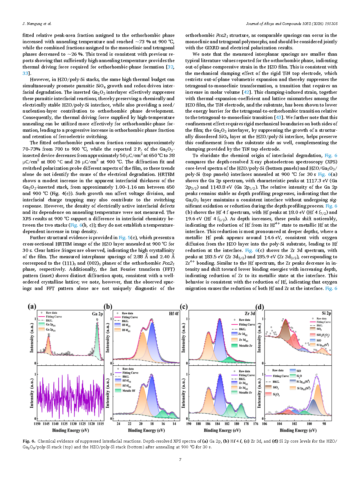
Suppression of interfacial redox reaction and parasitic SiOₓ growth:The Ga₂O₃ film works as an oxygen‑diffusion barrier, restraining oxygen migration from HZO to poly‑Si, suppressing parasitic SiOₓ thickening, mitigating Hf/Zr reduction and metallic defects, and alleviating polarization field screening.
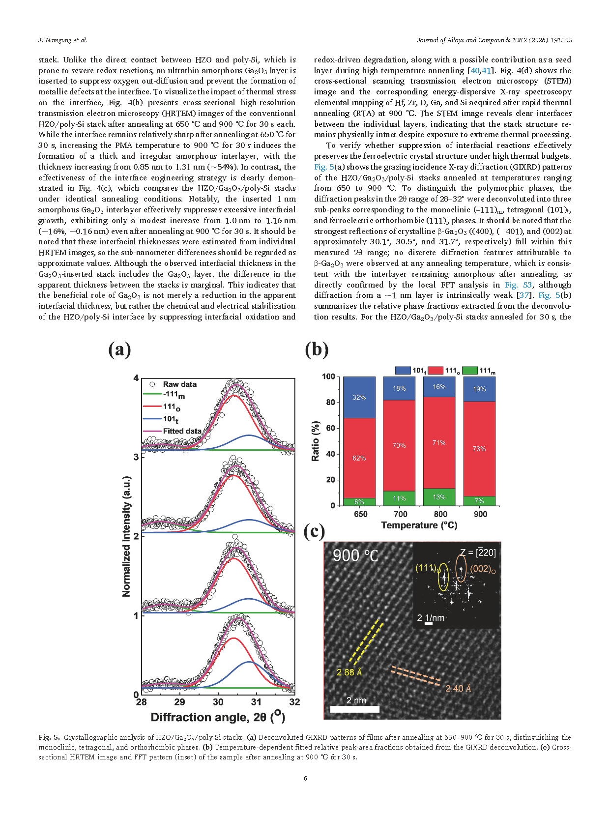
Preserve high fraction of ferroelectric orthorhombic phase after high‑temperature annealing:A high orthorhombic ferroelectric phase fraction (~73 %) is maintained for Ga₂O₃‑inserted stacks after 900 ℃ annealing, with observable ferroelectric switching, while reference devices without interlayer lose almost all switching capability.
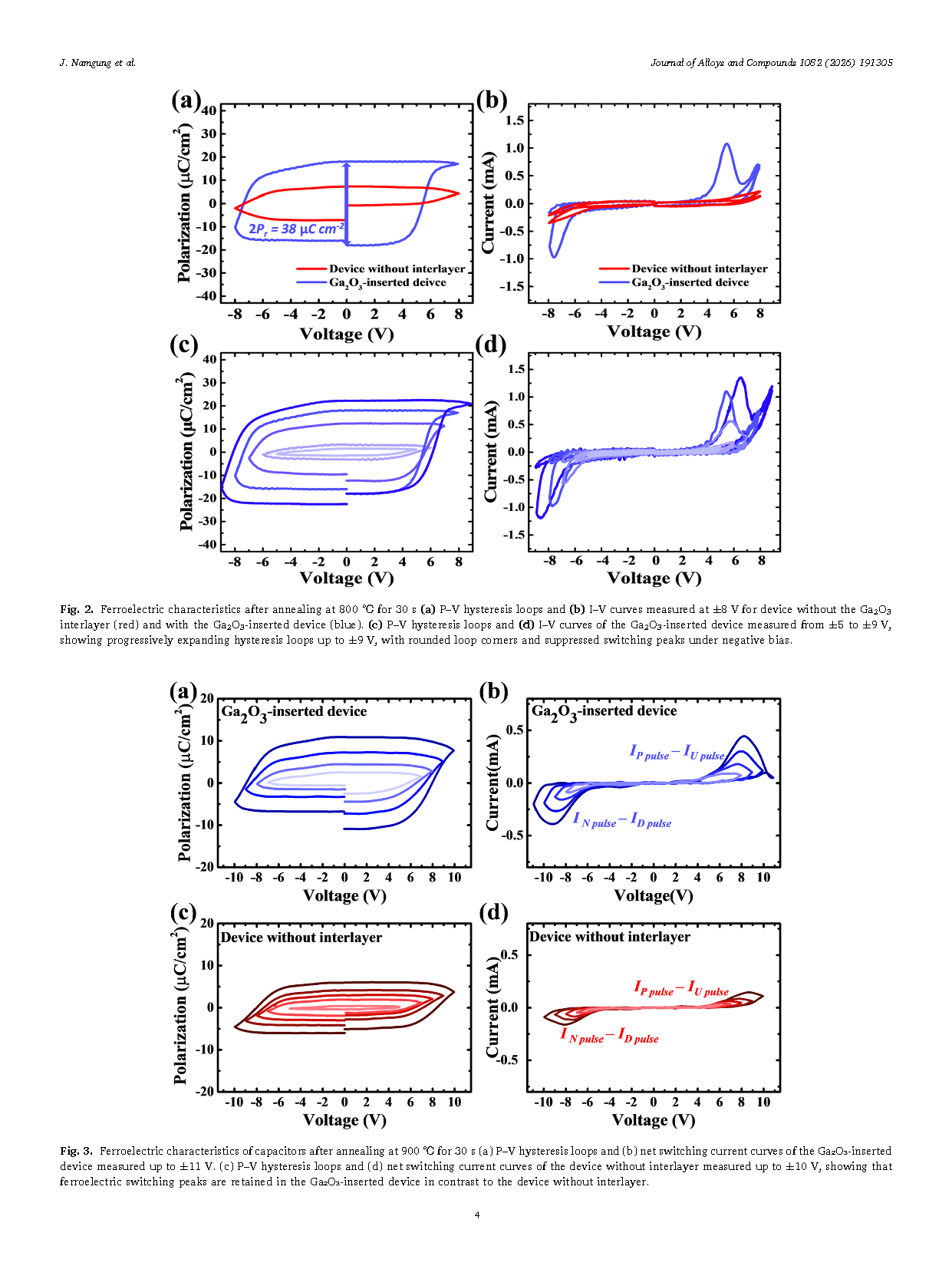
Outstanding ferroelectric electrical performance under high‑temperature condition:Excellent high‑temperature ferroelectric performance is achieved: 2Pᵣ ≈ 38 µC/cm² after 800 ℃ annealing and 2Pᵣ ≈ 26 µC/cm² even after 900 ℃ annealing, greatly outperforming reference samples.
Multiple characterization techniques to clarify physical‑chemical interfacial mechanism:Multiple characterization techniques including positive‑up‑negative‑down (PUND) electrical test, high‑resolution transmission electron microscopy (HRTEM), grazing‑incidence X‑ray diffraction (GIXRD), X‑ray photoelectron spectroscopy (XPS) and energy‑dispersive X‑ray spectroscopy (EDS) are adopted to clarify physical‑chemical interfacial‑modification mechanisms.
Conclusion
In this paper, we present a thermally robust TiN/HZO/poly-Si gate stack for 3D NAND process integration achieved by incorporating an ultrathin amorphous Ga₂O₃ interlayer. While devices without the interlayer suffered from severe interfacial degradation and strongly suppressed switching, consistent with interfacial reactions during high-temperature annealing, devices with the interlayer suppressed the interfacial redox reactions, maintained a high fitted orthorhombic peak-area fraction, and preserved ferroelectric switching with a 2Pᵣ of ~38 µC/cm² after annealing at 800 °C for 30 s and ~26 µC/cm² even after annealing at 900 °C for 30 s. These structural, chemical, and electrical observations support a barrier role for Ga₂O₃ in limiting interfacial reactions; oxygen transport and electrically active defect densities were not measured directly. Overall, these findings support the use of an amorphous Ga₂O₃ interlayer for improving the thermal-process compatibility of HZO ferroelectrics with poly-Si channels, providing a viable route toward next-generation 3D ferroelectric NAND flash technology.
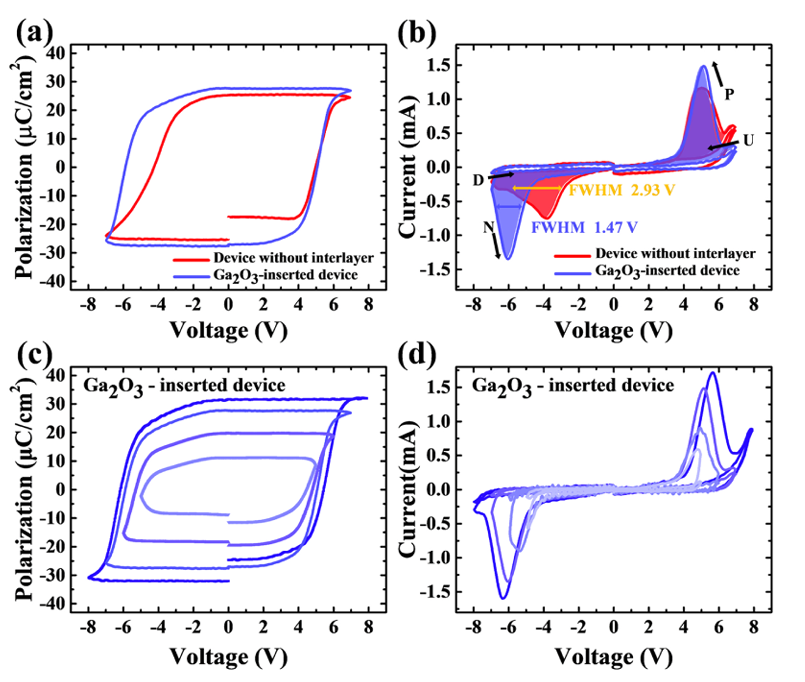
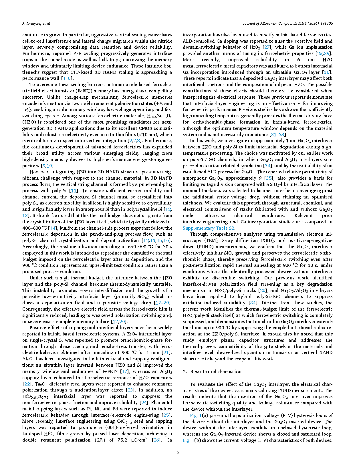
Fig. 1. Ferroelectric characteristics after annealing at 650 °C for 30 s (a) P-V hysteresis loops and (b) I-V curves measured at ±7 V for the device without the Ga₂O₃ interlayer (red) and with the Ga₂O₃-inverted device (blue). (c) P-V and (d) I-V curves of the Ga₂O₃-inverted device measured from ±5 V to ±8 V, showing a saturated loop up to ±7 V and the onset of an unclosed loop at ±8 V due to an additional high-field current contribution.
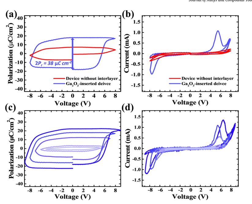
Fig. 2. Ferroelectric characteristics after annealing at 800 °C for 30 s (a) P-V hysteresis loops and (b) I-V curves measured at ±8 V for device without the Ga₂O₃ interlayer (red) and with the Ga₂O₃-inverted device (blue). (c) P-V hysteresis loops and (d) I-V curves of the Ga₂O₃-inverted device measured from ±5 to ±9 V, showing progressively expanding hysteresis loops up to ±9 V, with rounded loop corners and suppressed switching peaks under negative bias.
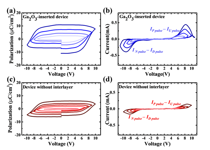
Fig. 3. Ferroelectric characteristics of capacitors after annealing at 900 °C for 30 s (a) P–V hysteresis loops and (b) net switching current curves of the Ga₂O₃-inverted device measured up to ±11 V. (c) P–V hysteresis loops and (d) net switching current curves of the device without interlayer measured up to ±10 V, showing that ferroelectric switching peaks are retained in the Ga₂O₃-inverted device in contrast to the device without interlayer.
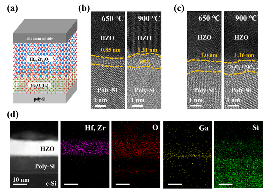
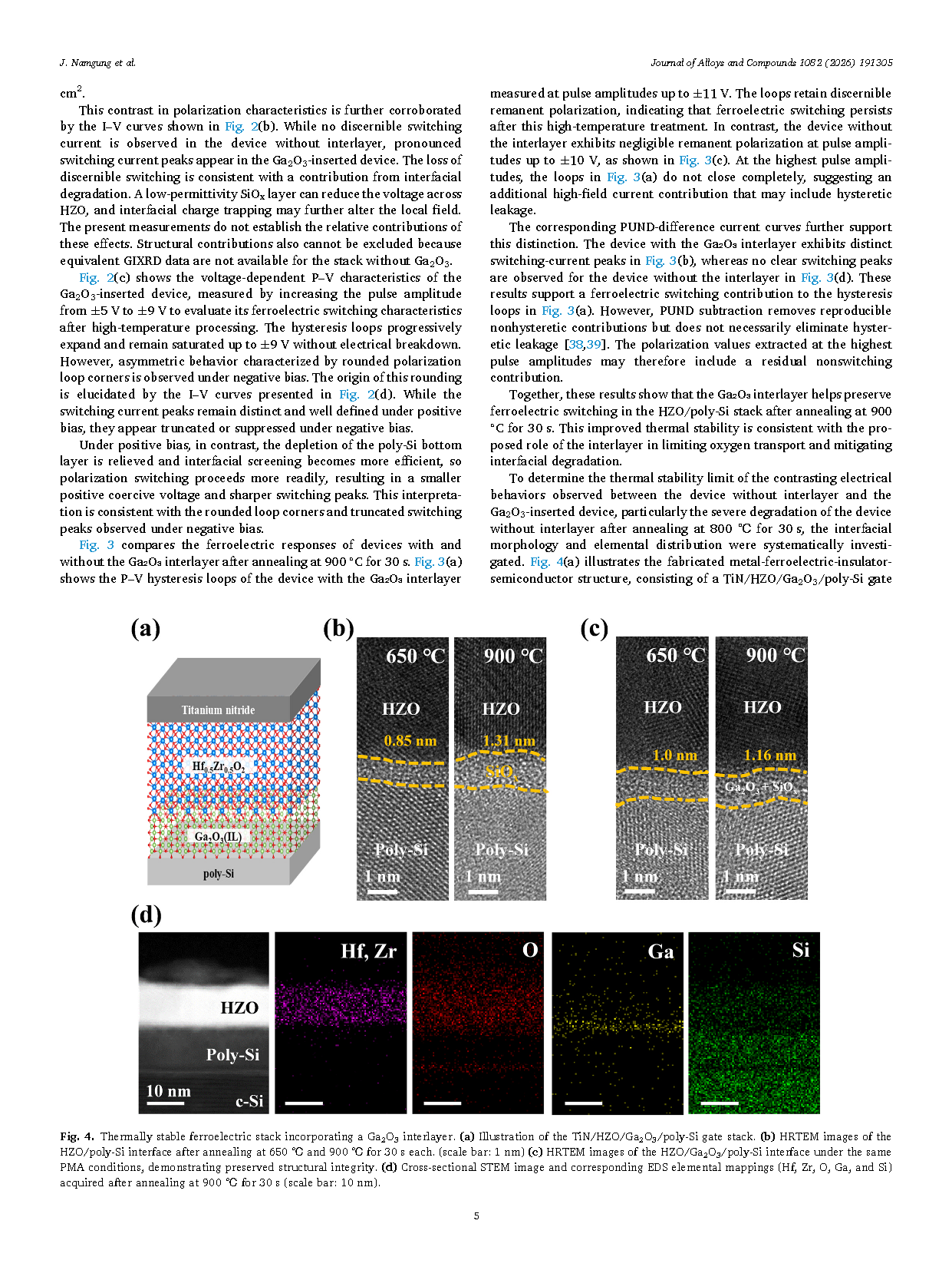
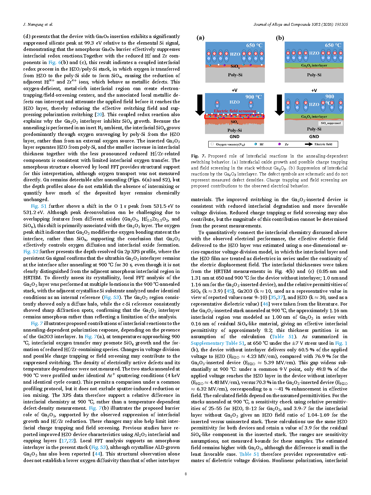
Fig. 4. Thermally stable ferroelectric stack incorporating a Ga₂O₃ interlayer. (a) Illustration of the TiN/HZO/Ga₂O₃/poly-Si gate stack. (b) HRTEM images of the HZO/poly-Si interface after annealing at 650 °C and 900 °C for 30 s each. (scale bar: 1 nm) (c) HRTEM images of the HZO/Ga₂O₃/poly-Si interface under the same PMA conditions, demonstrating preserved structural integrity. (d) Cross-sectional STEM image and corresponding EDS elemental mappings (Hf, Zr, O, Ga, and Si) acquired after annealing at 900 °C for 30 s (scale bar: 10 nm).
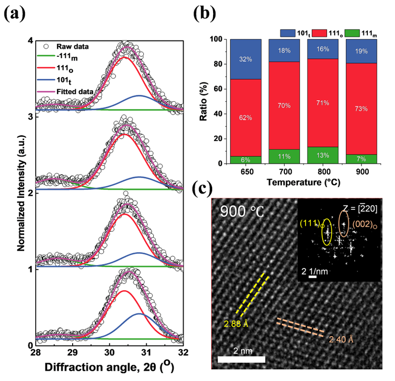
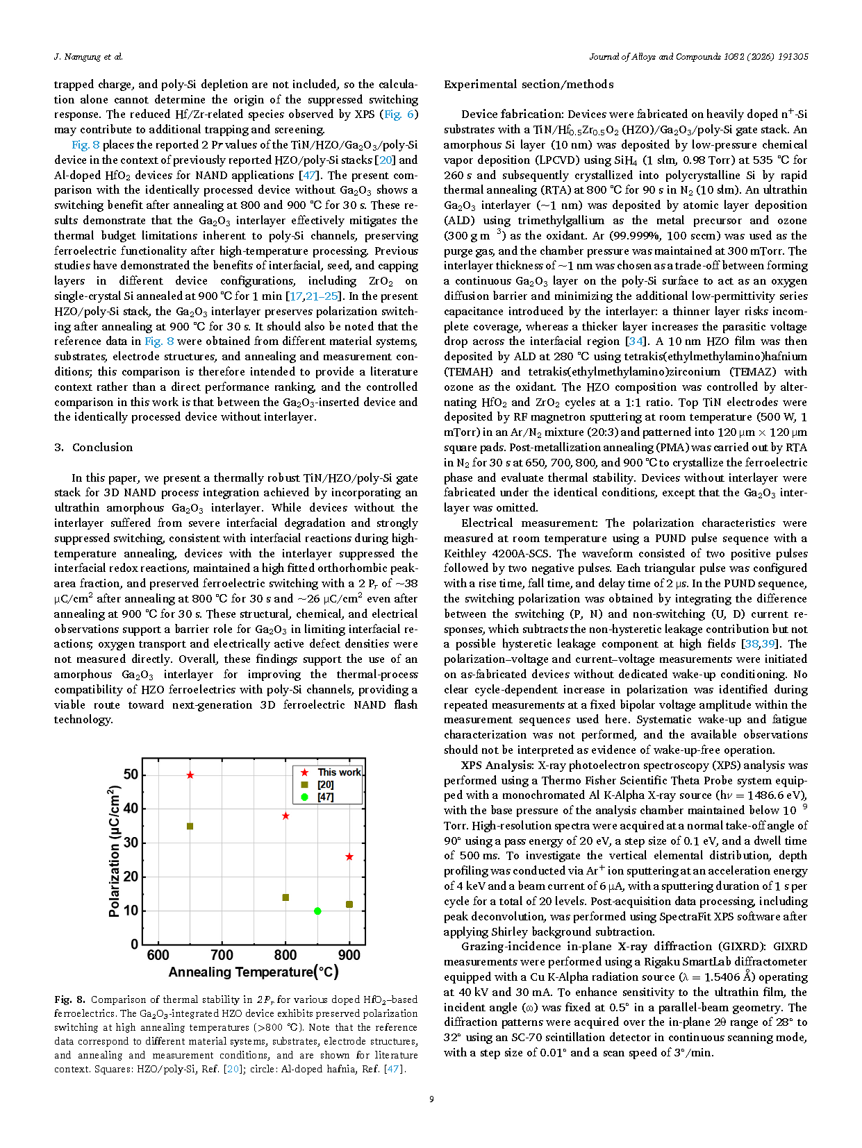
Fig. 5. Crystallographic analysis of HZO/Ga₂O₃/poly-Si stacks. (a) Deconvoluted GIXRD patterns of films after annealing at 650–900 °C for 30 s, distinguishing the monoclinic, tetragonal, and orthorhombic phases. (b) Temperature-dependent fitted relative peak-area fractions obtained from the GIXRD deconvolution. (c) Cross-sectional HRTEM image and FFT pattern (inset) of the sample after annealing at 900 °C for 30 s.
DOI:
10.1016/j.jallcom.2026.191305
Instruction
Official Account

Cooperation
Top
