

Where the Trillion-Yuan Integrated Circuit Industry Meets Fourth-Generation Semiconductors: A New Piece of the Materials Puzzle Takes Shape.
Jinjiang, a county-level city on the southeastern coast of Fujian Province, is renowned nationwide for its footwear and apparel industries. Yet in the integrated circuit sector, the city has long since moved beyond the role of a bystander. Two major industrial clusters—memory manufacturing and high-end semiconductor packaging and testing—have helped build an industry worth more than RMB 100 billion. With increasingly well-integrated and comprehensive supply chains, Jinjiang has repeatedly been cited as a model for semiconductor development at the county level. However, the larger the industrial landscape grows, the more conspicuous its gaps become. At the very upstream end of the value chain, both the supply of core epitaxial wafers for third-generation semiconductors and the commercialization of gallium oxide, a fourth-generation ultra-wide-bandgap semiconductor, have remained largely undeveloped for years.
Materials are the lifeblood of the semiconductor value chain. Demand for wide-bandgap semiconductors in applications such as new energy vehicles and 5G radio-frequency front ends is expanding at an exponential pace. Those who establish an early foothold in materials will secure a crucial entry point into the next generation of semiconductors. Jinjiang has clearly recognized this opportunity. From establishing talent and innovation funds to introducing targeted industrial policies and accelerating the development of specialized industrial parks, the city is deploying a coordinated set of measures to attract cutting-edge, technology-intensive startups.
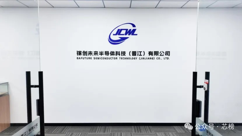
In late autumn 2025, a project quietly took root at Jinjiang Sanchuang Park. It was the first project funded by the Jinjiang Talent and Innovation Fund and the first gallium oxide epitaxial wafer R&D and manufacturing company established locally. Like a wedge, it filled one of the weakest links in Jinjiang’s semiconductor landscape. In less than a year, the company, GaFuture Semiconductor, has made simultaneous progress on four fronts: technology development, production line construction, team expansion, and market development, firmly establishing its presence in the early stages of China’s domestic gallium oxide industry.
GaFuture Semiconductor has completed the construction of a Class 10,000 cleanroom and is continuing to develop its gallium oxide epitaxial wafer production line and advance related R&D. Key performance indicators of the company’s 2-inch α- and β-phase gallium oxide epitaxial products are benchmarked against internationally advanced levels. The company has supplied samples to more than ten customers for evaluation and validation, and is steadily advancing its Pre-A financing round to accelerate the transition of its technological achievements into industrial applications.
Establishing a Presence in Jinjiang: A Rational Calculation of the Overall Costs and Benefits
From the initial idea to preparations for production line construction, GaFuture Semiconductor’s decision was not an impulsive move, but a calculated investment made after repeated comparisons of different options.
The initial connection came through the Jinjiang Talent and Innovation Fund, managed by Joint Capital. What ultimately convinced the team to commit, however, was a careful assessment of the overall costs and benefits. Jinjiang’s targeted support policies for the integrated circuit industry provide tangible financial assistance at multiple stages, from factory rent subsidies to electricity cost subsidies. Several leading semiconductor packaging, testing, and manufacturing companies have already established operations in the industrial park, placing upstream and downstream partners within easy reach. Combined with operating costs significantly lower than those in first-tier cities, these advantages proved decisive. For a deep-tech startup operating under tight cash-flow constraints, every penny must be spent wisely. Ultimately, these concrete cost-saving measures helped tip the balance in favor of establishing its epitaxial wafer production base in Jinjiang.
“Wherever a project is introduced, talent services follow.” This is how Dr. Peng Bo, founder of GaFuture Semiconductor, most directly describes his experience in Jinjiang. According to Dr. Peng, the team began its talent application process even before relocating, and seven team members were selected for Jinjiang’s Outstanding Talent Program for the Integrated Circuit Industry.
“Talent applications began before we even moved in. The policies and project recruitment efforts are closely coordinated, and the transition has been very smooth,” Dr. Peng said. However, he also pointed out that there is still room to accelerate the disbursement of industrial support funds, including subsidies for cleanroom renovation and equipment purchases. Faster policy implementation and earlier access to funding can provide much-needed support for startups while strengthening the city’s reputation as an attractive destination for investment. Such measures could also help more prospective projects move from hesitation to commitment.
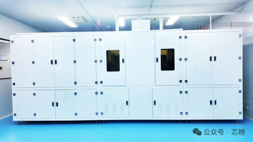
Gallium Oxide Heteroepitaxy Equipment
Technology as the Foundation: Advancing Four R&D Tracks in Parallel
Policy support provides the starting line, but technology is the real currency of competition. The gallium oxide industry is still in its early stages, and companies that establish a solid technological foundation first will be better positioned to gain a foothold in the market. From day one in Jinjiang, GaFuture Semiconductor has pursued a dual-track strategy, combining intensive R&D with the simultaneous establishment of production-line infrastructure.
Core Business Focus: Gallium Oxide Heteroepitaxy, with Sapphire and Silicon Carbide as Parallel Substrate Routes
On the one hand, the company continues to refine its growth processes, striving to push the limits of epitaxial layer crystal quality and uniformity. On the other, it is steadily scaling up wafer dimensions, progressing from initial 1 × 1 cm laboratory samples to 2-inch wafers and moving toward 4-inch wafers. Its heteroepitaxial technology on 2-inch sapphire substrates has now reached an internationally advanced level, while the silicon carbide substrate route has also yielded preliminary samples suitable for research at universities and scientific institutes. Building on these advances, the team is working intensively on p-type doping technology, seeking to bridge the final gap between theoretical concepts and experimental implementation and expand the range of device applications for gallium oxide materials.
Device Validation R&D: The Goal Is Not Mass Production, but Demonstrating Performance
The team is also advancing validation work on both power devices and radio-frequency (RF) devices. “We want to give customers a clear, tangible demonstration of performance and show that our materials can indeed be used to fabricate devices that meet the required specifications,” Dr. Peng explained.
To date, a Schottky barrier diode (SBD) fabricated using the company’s proprietary epitaxial wafers has completed wafer fabrication and testing, achieving a maximum breakdown voltage of 1,400 V. A surface acoustic wave (SAW) filter targeting consumer electronics has also completed device design and entered the wafer fabrication stage.
Production Capacity: Class 10,000 Cleanroom Completed, with Production Scheduled for the Second Half of 2026
Construction of the cleanroom has been completed, and equipment installation and commissioning for trial operations are nearing completion. The facility houses two hydride vapor phase epitaxy (HVPE) systems and two metal-organic chemical vapor deposition (MOCVD) systems, supporting different technological routes. This configuration can accommodate both R&D sample fabrication and small-batch production, providing a stable manufacturing foundation for continued technological iteration and customer delivery.
The Talent Challenge: Practical Workarounds and Real Pain Points for a County-Level Startup
As the company’s technical roadmap and production plans gradually take shape, team building and market development are also moving forward at a rapid pace.
Yet people remain the biggest variable.
At the high-end R&D level, talent is already scarce across the gallium oxide sector. Core positions generally require at least a master's degree from a top-tier Chinese university, such as those in the 985 or 211 university programs. These candidates tend to be more accustomed to the industrial ecosystems of the Yangtze River Delta and Pearl River Delta, while Jinjiang has relatively limited appeal as a place to live and work. Even when salary expectations are met, many candidates remain hesitant because of concerns about local amenities and lifestyle. For production-line operations, Jinjiang does have a pool of talent developed by leading local companies. However, the salary benchmarks set by these industry leaders have also pushed up overall labor costs, while recruitment from other regions often falls through because of distance and difficulties adapting to local life.
On the market front, the company currently relies on alumni and shareholder networks associated with Xidian University to develop business, focusing primarily on power devices and RF devices. Its customer base includes universities and research institutes such as Xi'an Jiaotong University, Xidian University, and North University of China. Revenue currently comes mainly from sample evaluation and small-batch sales. Dr. Peng candidly acknowledged that this reflects a challenge shared across the industry: gallium oxide technology remains in the validation stage, commercial demand has yet to emerge on a large scale, and research-related orders are still unstable.
Throughout this process, Dr. Peng has maintained a clear-eyed view of the competitive landscape:
“There are around a dozen companies in China working on gallium oxide substrates and epitaxy, including five or six specializing in epitaxy. Almost none have reached mass production of devices. This is not yet a stage where we are dividing up the pie; it is a stage where we all need to make the pie bigger. A single company cannot persuade downstream customers to switch materials on its own. Only through collective efforts to promote the technology can we open up the market.”
Assessing the Industry Cycle: Patience Without Rushing Ahead or Engaging in Cutthroat Competition
The company is not rushing to secure short-term orders or blindly pouring money into capacity expansion. This discipline stems from Dr. Peng Bo’s long-term assessment of the gallium oxide industry cycle.
“Commercialization at scale will most likely begin around 2028,” he said.
His assessment is based on the development trajectory of the silicon carbide industry. Taking a power device from initial trials to resolving reliability issues and achieving large-scale deployment typically requires four to five years of technological refinement. Automotive-grade applications take even longer, involving the validation of hundreds of parameters one by one, some of which may even be mutually incompatible. The process of fine-tuning these parameters can take years.
In terms of material dimensions, 2-inch wafers remain the industry mainstream, while 4-inch wafers are still relatively uncommon. Achieving the level of industrial maturity required for 6-inch wafers will take several more years of iterative development.
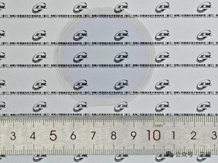
2-Inch Sapphire-Based Gallium Oxide Heteroepitaxial Wafer
The global competitive landscape also warrants scrutiny. Japan and the United States entered the field earlier and have a first-mover advantage in materials development. However, gallium oxide was added to the Wassenaar Arrangement’s control list in 2019, restricting the sale of high-end products to China. This has, in turn, created an opportunity for domestic companies to develop their own technologies and capabilities.
Most overseas products that can currently be obtained in China through indirect channels are from discontinued or outdated production batches, making it difficult to assess the true technological gap. Based on the samples available, overseas materials do have an advantage, but the lead appears limited. Moreover, after passing through multiple intermediaries, a single 2-inch substrate can cost as much as RMB 20,000—more than twice the price of a domestic product.
China’s distinctive advantage, by contrast, lies in its upstream raw materials. Gallium is a by-product of aluminum electrolysis. As developed economies have gradually withdrawn from aluminum electrolysis due to its high energy consumption and environmental impact, China has come to account for a major share of global gallium production capacity, giving it considerable influence over the raw material supply chain.
Recommendations for County-Level Development: How to Build and Retain a Semiconductor Ecosystem
After nearly a year of establishing its presence in Jinjiang, GaFuture Semiconductor has gained firsthand experience of the city’s semiconductor ecosystem while growing its own business. Peng Bo believes that technology-driven companies consider three key factors when choosing a city: funding, talent, and industrial resources. Only when these three elements work together can a city build lasting appeal.
Funding: He recommends improving the speed at which industrial subsidies and incentives are disbursed, while simplifying approval procedures. This would enable startups to access support sooner and ease cash flow pressures. “When policies are implemented promptly, companies gain confidence. As word spreads, more projects will be willing to come, creating a positive cycle.”
Talent: He advocates a two-pronged approach that combines attracting talent from outside with developing it locally. On the recruitment side, cities should improve compensation packages and accelerate the disbursement of talent subsidies to make themselves more attractive to high-caliber professionals. On the training side, there is no need to rush into developing top-tier R&D talent from the outset. Instead, cities can begin by addressing the need for entry-level production-line personnel. Local vocational colleges could introduce integrated circuit-related programs, enabling students to become familiar with cleanroom protocols and basic operations while still in school. This would allow graduates to enter the workforce immediately and shorten companies’ training cycles. Meanwhile, leading companies could establish joint laboratories with universities, providing funding for equipment and consumables to ease universities’ research funding pressures while training talent specifically suited to local industry needs.
“County-level regions face inherent disadvantages in developing the semiconductor industry. But with pragmatic policies and effective services, they can still attract projects and talent.” Peng Bo said. GaFuture Semiconductor will continue to put down roots in Jinjiang, advancing its gallium oxide epitaxy technologies while exploring pathways to commercialization. Step by step, the company aims to grow alongside the city’s integrated circuit industry ecosystem.
Instruction
Official Account

Cooperation
Top