


Researchers from the Incheon National University have published a paper titled "Flexible and Transparent Ga₂O₃/NiO Photovoltaic Diode for Full-Wave Rectification in Wearable Optoelectronics" in Advanced Electronic Materials.
Background
Flexible and transparent electronic components are critical for next-generation wearable optoelectronic devices, which require lightweight, flexible, and optically transparent power solutions. Wearable systems commonly operate using direct current. Triboelectric and piezoelectric nanogenerators produce alternating current, which requires efficient AC-to-DC conversion for practical application. Conventional silicon-based rectifiers are not suitable for flexible transparent electronics due to rigidity and opacity.
Wide-bandgap oxide semiconductors can be fabricated at low temperature and are compatible with flexible polymer substrates. Amorphous Ga₂O₃ has an ultra-wide bandgap, and NiO acts as a stable transparent p-type semiconductor. The constructed p-n heterojunction shows outstanding rectifying performance. Nevertheless, achieving efficient full-wave rectification together with high optical transmittance and good mechanical flexibility remains a major technical challenge. In this work, Ga₂O₃/NiO heterojunction photovoltaic diodes are fabricated on PET flexible substrates. The optoelectronic and bending mechanical properties are investigated. The diodes are integrated into full-wave rectifier circuits to verify their application potential in self-powered wearable optoelectronic devices.
Abstract
Flexible and transparent electronic components are critical for next-generation wearable optoelectronic devices, which require lightweight, flexible, and optically transparent power solutions. Wearable systems, including smart textiles, flexible displays, and bioelectronics, commonly operate using direct current (DC). While transparent photovoltaics can directly generate DC power under illumination, triboelectric and piezoelectric nanogenerators produce alternating current (AC), requiring efficient AC-to-DC conversion for practical use. However, conventional silicon-based rectifiers are unsuitable for flexible transparent electronics because of their rigidity and opacity. This study presents a flexible and transparent Ga₂O₃/NiO heterojunction photovoltaic diode array functioning as a full-wave rectifier for wearable optoelectronic applications. The sputter-deposited device exhibits 65% optical transparency in the visible region, a low leakage current of 1.07 nA, and a rectification ratio of 8.505 ×10³ at ± 2 V. Under ultraviolet-C (UVC) illumination, the device demonstrates photovoltaic energy harvesting with an open-circuit voltage of 462 mV and a short-circuit current density of 103.08 μA cm⁻². It also shows self-powered photodetection performance with a responsivity of 13 mA W⁻¹ and a detectivity of 2.43 ×10¹¹ Jones. Integration into a full-wave rectifier successfully enables AC-to-DC conversion, highlighting its potential for transparent, flexible, and self-powered wearable devices.
Highlights
① Sputtered Ga₂O₃/NiO p-n heterojunction is realized on PET flexible substrate, delivering high visible-light transmittance and favorable diode rectifying characteristics simultaneously.
② The heterojunction device possesses dual functions including photovoltaic energy harvesting and solar-blind UV self-powered photodetection, with high responsivity and detectivity.
③ The device exhibits good mechanical tolerance and maintains rectifying performance after repeated bending, suitable for dynamically deformed wearable scenarios.
④ Flexible transparent Ga₂O₃/NiO diodes are successfully integrated into full-wave rectifier circuits to realize AC-DC signal conversion.
⑤ Integration of photovoltaic generation and rectifying units provides a new device solution for next-generation transparent self-powered wearable optoelectronic devices.
Conclusion
An integrated device was developed, combining photovoltaic energy generation with a transparent and flexible full-wave rectifier, utilizing the Ga₂O₃/NiO heterojunction architecture. Under 265 nm illumination at an intensity of 7.9 mW cm⁻² the device demonstrated robust photovoltaic characteristics, achieving an open-circuit voltage of 462 mV and a short-circuit current density of 103.08 μA cm⁻². Additionally, it demonstrated a responsivity of 13 mA W⁻¹ and detectivity of 2.43 ×10¹¹ Jones. The heterojunction displayed an ideality factor of 1.59, a rectification ratio of 8.505 ×10³ at ± 2 V, and a low reverse leakage current of 1.07 nA, even under mechanical bending conditions, though excessive bending introduces strain-related damage that compromises junction integrity and rectification performance. However, the synergy of photovoltaic and rectification performances, combined with high optical transparency and mechanical flexibility, positions this device as a strong candidate for next-generation flexible transparent electronics. The integration of wide-bandgap Ga₂O₃ with p-type NiO facilitated the formation of a high-performance rectifying junction while ensuring minimal optical loss across the visible spectrum. Furthermore, the rectifier consistently maintained stable electrical characteristics during repeated bending, highlighting its suitability for dynamic and deformable electronic systems. Overall, these results establish a promising pathway toward the development of transparent, lightweight, and mechanically robust electronic components, with potential applications in flexible sensors, energy-harvesting circuits, and wearable photonic devices.
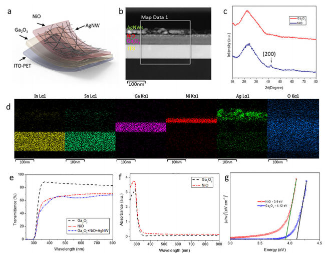
Figure 1. (a) Schematics of Ga₂O₃/NiO-based flexible diode structure. (b) TEM image of the cross-section of the ITO-Ga₂O₃/NiO-AgNWs diode. (c) XRD spectra of Ga₂O₃ and NiO films on the glass substrate. (d) EDS mapping and corresponding distribution of In, Sn, Ga, Ni, Ag, and O in the diode structure. (e) Transmittance spectra of Ga₂O₃, NiO, and Ga₂O₃+NiO+AgNWs layers, (f) absorbance spectra of the Ga₂O₃ film, NiO film, and Ga₂O₃ + NiO + AgNWs layers, and (g) Tauc plots indicating the values of 4.12 and 3.9 eV for the Ga₂O₃ and NiO films, respectively.
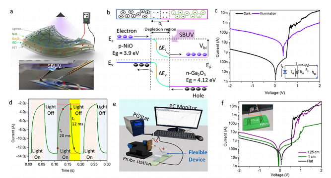
Figure 2. (a) Schematic of transparent Ga₂O₃/NiO diode under light illumination, (b) Band diagram of Ga₂O₃/NiO heterojunction, (c) I-V curve of Ga₂O₃/NiO showing the characteristics under dark and light illumination, (d) transient current response under 250 nm light illumination with rise time and fall time, (e) schematic of transparent Ga₂O₃/NiO diode bending test measurement setup (f) Dark current response for the bending position of 1.25 and 1 cm radius and flat. Inset schematic of transparent Ga₂O₃/NiO diode bending test measurement setup.
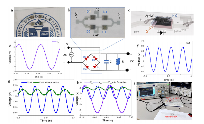
Figure 3. (a) Real image of the Ga₂O₃/NiO diode-based transparent flexible rectifier circuit, (b) element and connection alignment of the fabricated Ga₂O₃/NiO diode-based transparent flexible rectifier circuit, (c) schematic of a single diode connection in the rectifier circuit, (d) input voltage to the rectifier circuit, (e) schematic of the rectifier with a 10 KΩ resistor and 25 V 220 µF capacitor, connected in parallel with the output, (f) output ripple DC voltage, (g) output voltage after smoothing (red curve) using a 25 V 220 µF smoothing capacitor, compared with the output ripple DC voltage, (h) comparison of the input AC voltage, output ripple DC signal, and smoothing DC signal, and (i) real image of circuit connection setup.
Figure 4. Setup of the flexible and transparent wearable Ga₂O₃/NiO diode-based rectifier circuit as wearable electronics.
DOI:
10.1002/aelm.70587
Instruction
Official Account

Cooperation
Top
