


Researchers from Xidian University have published a dissertation titled " Orientation-dependent interface-state properties underlying the “V”-shaped difference in temperature-dependent reverse characteristics of [010]- and [100]-oriented trench-MOSSBDs " in Applied Physics Letters.
Background
β-Ga₂O₃, offering a high critical field (8 MV/cm) and low-cost substrates, is a leading candidate for next-generation power devices. MOS-type trench structures enable 3-D field distribution, mitigate crowding, and avoid conductive p-type doping, pushing breakdown voltages beyond 3 kV toward theoretical BFOM limits. However, strong crystallographic anisotropy makes dry-etch-induced sidewall interface states especially severe in the [100] orientation. Existing trench devices therefore favor the [010] orientation despite its lower sidewall thermal conductivity, leaving the higher-conductivity [100] orientation largely unused. Prior work has mainly examined [010] interface states; the orientation-dependent impact on reliability and the underlying mechanisms remain unclear. Conventional DLTS further struggles to distinguish interface states from bulk traps when their emission time constants overlap. Elucidating orientation-dependent interface-state properties and enabling electro-thermal/reliability co-design in anisotropic β-Ga₂O₃ trenches is thus an urgent need.
Abstract
In β-Ga₂O₃ MOS-type trench diodes, electro-thermal performance is strongly limited by poor trench-sidewall interface quality induced by anisotropic dry etching. This issue is more pronounced in [100]-oriented trenches, which exhibit higher sidewall thermal conductivity than [010]-oriented trenches. However, the orientation-dependent impact of interface states on device reliability and the underlying physical mechanisms remain unclear. This work elucidates, for the first time, the orientation-dependent interface-state properties responsible for the distinctive “V”-shaped temperature dependence of the reverse I–V characteristics between [010]- and [100]-oriented β-Ga₂O₃ trench MOS- type Schottky barrier diodes (trench-MOSSBDs) with HfO2 dielectric. Within the low-temperature range (25–125℃), the “V”-shaped behavior in [100]-oriented trench-MOSSBD originates from the temperature-dependent competition between slow and fast interface-state charge trapping/de-trapping processes, whereas the reverse characteristics of [010]-oriented trench-MOSSBDs are predominantly governed by fast interface states. These findings provide important physical insights into interface-state engineering in anisotropic β-Ga₂O₃ trench structures and offer guidance for the electro-thermal co-design of high-performance β-Ga₂O₃ trench power devices.
Highlights
In the past, [010] orientation was predominantly adopted for β-Ga₂O₃ trench devices due to the poorer sidewall interface quality caused by [100] dry etching; however, this simultaneously forfeited the advantage of higher thermal conductivity of the [100] trench sidewall. This work extends the description of this reliability trade-off from the phenomenon of "higher interface state density" to a verifiable physical image for the first time: within the temperature range of 25–125 °C, the "V" shape of the reverse characteristics of [100] oriented trench-MOSSBD originates from the competition between slow and fast interface state charge trapping/releasing with temperature; the reverse characteristics of the [010] orientation are primarily dominated by fast interface states. Additionally, to address the issue where conventional DLTS struggles to uniquely identify the source of defects when the emission time constants of bulk traps and interface states overlap, this work employs a complementary approach combining pulsed C-V, ultraviolet-assisted C-V, device forward thermoelectric coupling modeling, and DLTS, achieving comparative characterization of interface states for both orientations. The implication for device design derived from this is that electro-thermal synergy cannot solely rely on thermal conductivity or dielectric anisotropy. If the slow deep interface states of the [100] orientation can be reduced through interface passivation, post-etching treatment, and dielectric processes, it may be possible to simultaneously leverage its sidewall thermal conductivity advantage while maintaining acceptable reverse reliability. The aforementioned results provide a physical basis for the interface state engineering of anisotropic β-Ga₂O₃ trench structures and guidance on orientation selection for the electro-thermal synergy design of high-performance β-Ga₂O₃ trench power devices.
Conclusion
In conclusion, this work reveals the physical mechanism by which orientation-dependent etch-induced interface states lead to “V”-shaped differences in temperature-dependent reverse I–V characteristics of [010]- and [100]-oriented trench-MOSSBDs. Ultimately, this finding can pave the way for interface-state engineering in anisotropic β-Ga₂O₃ trench structures and effective electro-thermal codesign in β-Ga₂O₃ trench devices, which will be instrumental in improving both device performance and reliability in the future.
Project Support
This work was supported by the NSFC under Grant No. 62204187.
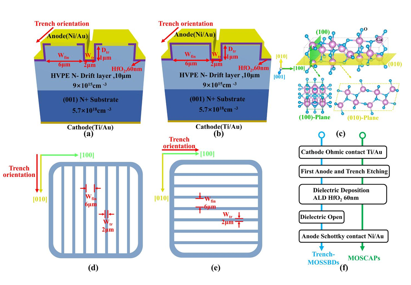
FIG. 1. Schematic cross-sectional diagram of (a) trench-MOSSBDs and (b) MOSCAPs. (c) β-Ga₂O₃ crystal structure and the corresponding crystal planes. (d) and (e) Schematics (top view) of trench- MOSSBDs and MOSCAPs with trench along [010] and [100] orientations, respectively. (f) Fabrication process flow of trench-MOSSBDs and MOSCAPs.
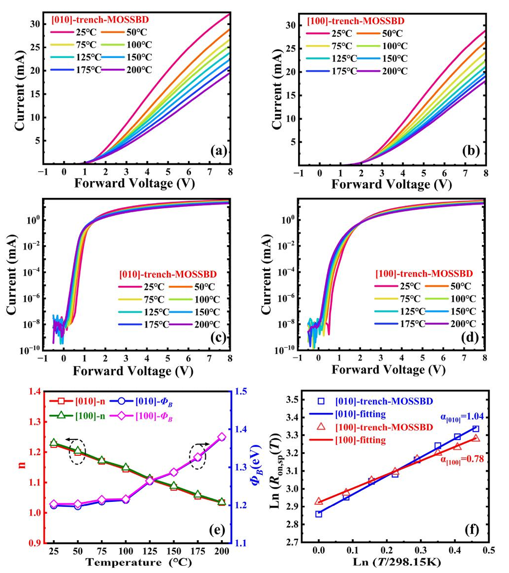
FIG. 2. Temperature-dependent forward I–V characteristics of [010]-oriented (a) and (c) and [100]-oriented (b) and (d) trench-MOSSBDs in linear scale (a) and (b) and semi-log scale (c) and (d). Temperature-dependent (e) n and ΦB, and (f) Ron,sp of trench-MOSSBDs.
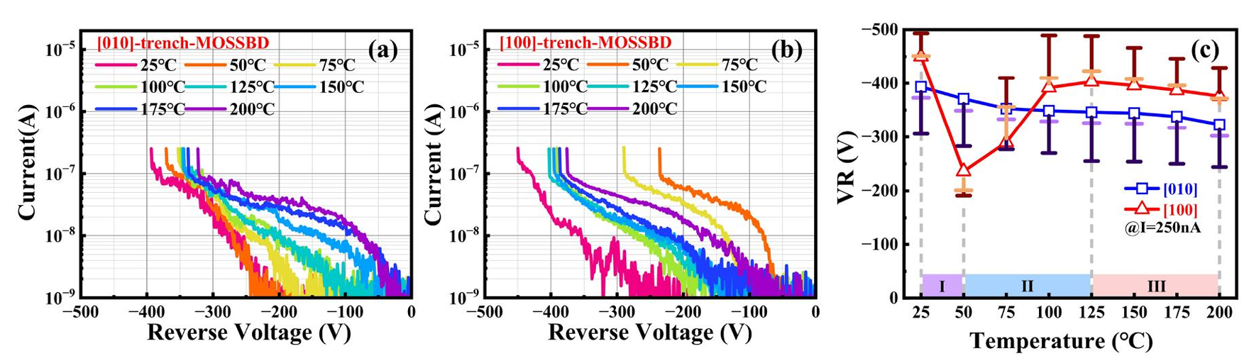
FIG. 3. Temperature-dependent reverse I–V characteristics of (a) [010] and (b) [100]-oriented trench-MOSSBDs, along with (c) temperature-dependent VR with error bars.
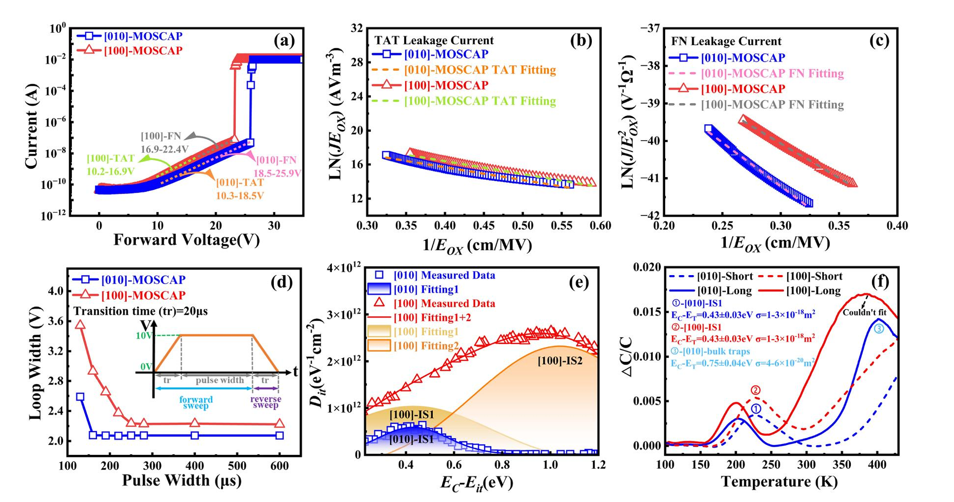
FIG. 4. (a) Forward I–V characteristics of [010]- and [100]-oriented MOSCAPs. (b) TAT and (c) FN leakage mechanism. (d) Loop width vs pulse width curves (inset: pulse C-V waveform). (e) UV-assisted C–V and (f) DLTS results of MOSCAPs.
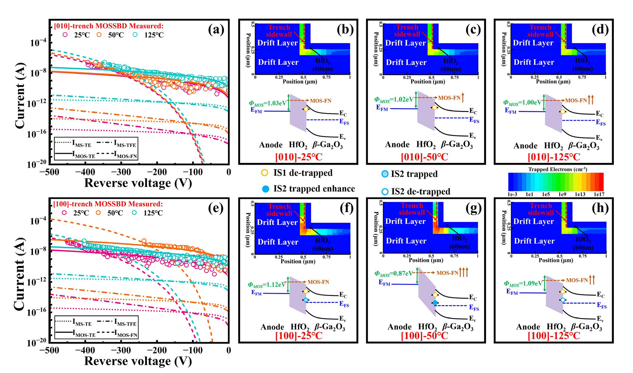
FIG. 5. (a) and (e) Measured reverse I–V characteristics and calculated reverse I–V at 25, 50, and 125℃ for trench-MOSSBDs. (b)–(d) and (f)–(h) Corresponding simulated trapped electrons profiles (top) and energy band diagrams (bottom) along the trench sidewall at three temperatures under high reverse bias.
DOI:
doi.org/10.1063/5.0344720
Instruction
Official Account

Cooperation
Top
