

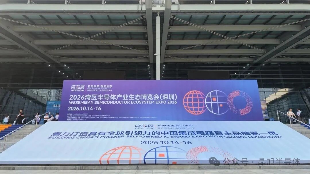
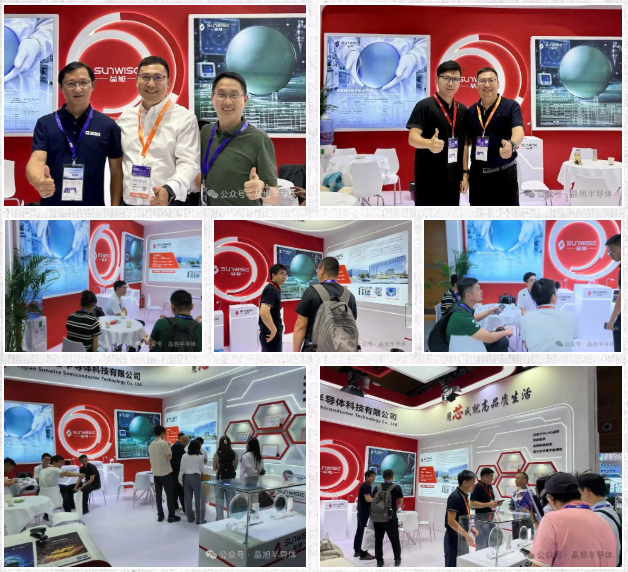
From October 14 to 16, 2026, the WESEMiBay Semiconductor Ecosystem Expo 2026 opened grandly at the Shenzhen Convention and Exhibition Center. Nearly 1,000 semiconductor companies from 22 countries and regions gathered at the event to explore opportunities in a new trillion-yuan growth cycle.
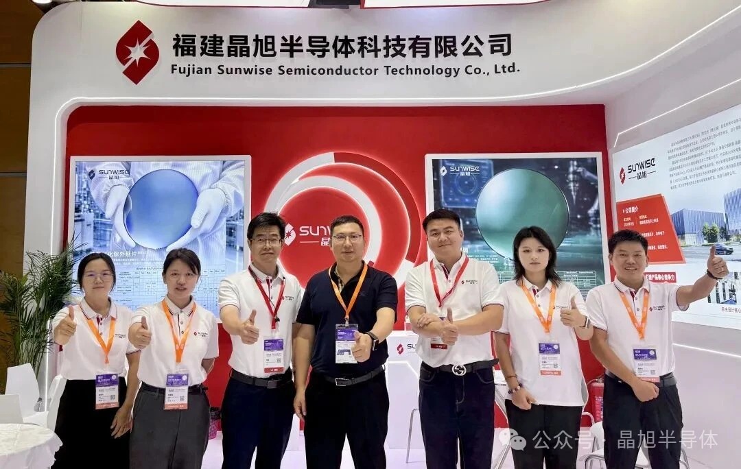
Fujian Sunwise Semiconductor Technology Co., Ltd. showcased two major product series, highlighting its industrialization achievements in high-speed optical communications and ultra-wide-bandgap semiconductor materials for radio-frequency applications.
Advancing Foundational Materials and Building a Dual-Track Product Portfolio
Fujian Sunwise Semiconductor's exhibits span two major application areas—optical communications and radio frequency (RF)—showcasing a comprehensive product chain from wafer materials to device applications.
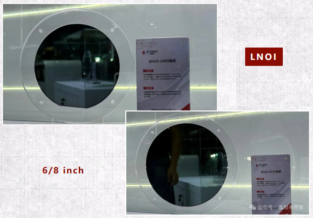
In the field of high-speed optical interconnects, Sunwise showcased its LNOI wafers and SOI silicon photonics wafers. Leveraging its proprietary plasma-based precision film thickness control technology, these products offer outstanding characteristics, including ultra-thin films, high coplanarity, and low surface roughness. They are well suited for data center and long-distance optical interconnect applications, with further potential in emerging fields such as quantum optics, microwave photonics, and acoustic filtering.
Among these products, SOI silicon photonics wafers serve as a key platform for optical interconnects in data centers, with their penetration in 800G and higher-speed products continuing to increase.
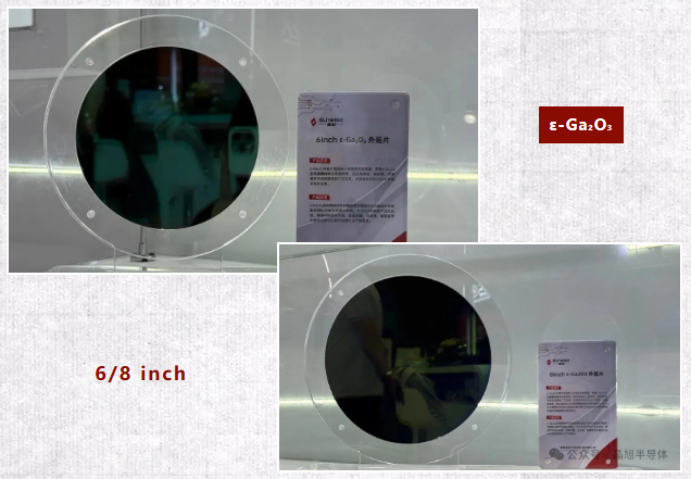
In the RF segment, Sunwise showcased its ε-Ga₂O₃ epitaxial wafers and POI wafers. With more than 20 years of experience in acoustic wave filter technology, the company's technical team has overcome key challenges in silicon-based heteroepitaxy and thin-film transfer. In 2023, this material system earned the highest award in the final round of China's National Disruptive Technology Innovation Competition.
ε-Ga₂O₃ piezoelectric films offer large-area single-crystal structures, a high piezoelectric coefficient, and significant cost advantages. The resulting POI wafers are precisely tailored to the performance requirements of film bulk acoustic resonator (FBAR) and solidly mounted resonator bulk acoustic wave (SMR-BAW) filters, providing a new foundational materials solution for 5G/6G RF applications requiring wide bandwidth and low loss.
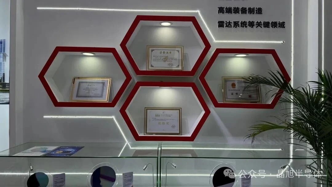
The joint presentation of these two product series reflects Sunwise Semiconductor's strategic focus on two business segments: optoelectronic integration and gallium oxide-based RF technologies.
Exploring Industry Collaboration and Building a Thriving Semiconductor Ecosystem
As a provider of advanced domestic semiconductor materials and wafer solutions, Fujian Sunwise Semiconductor will continue to deepen its focus on optical communications and ultra-wide-bandgap semiconductors. By advancing proprietary core processes, the company aims to overcome fundamental material bottlenecks and work with partners to break through international barriers in critical materials and devices. It is committed to driving the steady development of core materials for high-end chips and optical communication products, with the vision of becoming a world-leading company in compound semiconductor R&D, manufacturing, and services.
About Sunwise Semiconductor
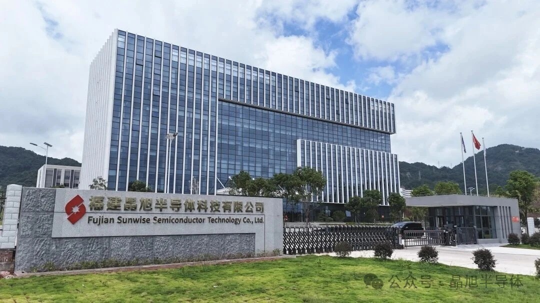
Sunwise Semiconductor focuses on ultra-wide-bandgap semiconductor and optoelectronic integration technologies based on third-generation gallium nitride (GaN) and fourth-generation gallium oxide (Ga₂O₃) materials. The company is a high-tech enterprise with rare wafer-level heterogeneous and heterostructure integration capabilities in China.
Led by an academician-backed R&D team, Sunwise has developed proprietary technologies for single-crystal Ga₂O₃ thin-film epitaxy and wafer-level heterogeneous integration, with more than 100 core patents and a comprehensive portfolio of independently owned intellectual property.
Leveraging its advanced heterogeneous integration platform, Sunwise has established an end-to-end process chain covering epitaxial growth, damage-free thin-film release, wafer-level transfer and bonding, and optoelectronic integration and packaging. Its 8-inch-class wafer-level heterogeneous integration platform is aligned with the process requirements of optical communication modulator chips. The company has achieved volume production and delivery of GaN optoelectronic integration packaging, while its 6- and 8-inch Ga₂O₃ epitaxy and substrate-transfer product lines, including Ga₂O₃ POI wafers, are entering pilot production and ramp-up stages.
Looking ahead, Sunwise plans to extend its heterogeneous integration technologies to thin-film lithium niobate on insulator (LNOI) and silicon-on-insulator (SOI) platforms for AI computing optical modules. The company is committed to working with industry partners to address key bottlenecks in advanced semiconductor materials and devices, helping overcome international technology barriers and supporting the development of high-end chip materials and optical communication products. Its goal is to become a world-leading company in compound semiconductor materials R&D, manufacturing, and services.
Instruction
Official Account

Cooperation
Top