


FLOSFIA, a startup originating from Kyoto University, has successfully grown an epitaxial α-Ga₂O₃ film on a 6-inch (150 mm) sapphire substrate, achieving approximately ±3% in-plane thickness uniformity. The company is advancing the world's first practical implementation of gallium oxide (α-Ga₂O₃) power semiconductors.
The 6-inch wafer diameter is widely used in mass production of silicon carbide (SiC) power semiconductors. By leveraging existing 6-inch production lines, partners can accelerate the launch of mass production for gallium oxide power semiconductors. Furthermore, based on results obtained with 3- to 6-inch wafers, FLOSFIA has confirmed that in-plane thickness uniformity of within ±4% is expected to be achievable on 8-inch (200 mm) wafers.
Following the demonstration of its 4-inch wafer manufacturing technology announced in December 2025, this achievement marks further progress in scaling up low-temperature, atmospheric-pressure epitaxial growth using the company's proprietary Mist Dry® method. Building on this milestone, FLOSFIA aims to accelerate the commercialization of gallium oxide power semiconductors, positioning the technology as a leading candidate for the post-SiC era.
Background: Increasing Wafer Diameter in Power Semiconductors
The power semiconductor industry is expanding wafer diameters to increase the number of chips obtainable from each wafer and reduce manufacturing costs.
Currently, 6-inch wafers are widely used in mass production of SiC power semiconductors, while some manufacturers have begun transitioning to 8-inch wafers. Silicon (Si)-based power semiconductors predominantly use 8-inch production lines, with some facilities employing 12-inch wafers.
For new semiconductor materials to be adopted by power semiconductor manufacturers, compatibility with existing mass-production lines is an important requirement.
Achievement: Epitaxial Growth on 6-Inch Sapphire Substrates
FLOSFIA modified its Mist Dry® method and successfully deposited an α-Ga₂O₃ epitaxial film on a 6-inch sapphire substrate.
The resulting film achieved approximately ±3% in-plane thickness uniformity, meeting the initial commercialization target of within ±4%. The film was also free of cracks and exhibited a low density of foreign-particle defects, indicating good overall quality.
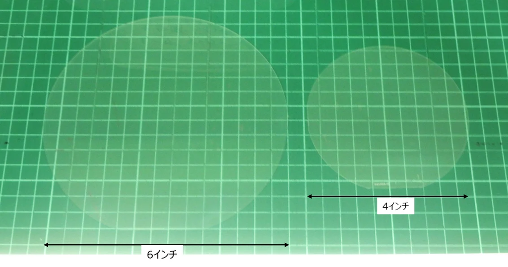
Figure 1. α-Ga₂O₃ epitaxial wafer grown on a 6-inch sapphire substrate (left) and a 4-inch wafer (right).
Outlook for 8-Inch Wafer Manufacturing
By comparing in-plane thickness uniformity across 3-, 4-, and 6-inch wafers, the research team found that thickness variation increases as wafer diameter grows, but the rate of increase gradually decreases.
Based on this trend, FLOSFIA expects to achieve in-plane thickness uniformity within ±4% on 8-inch (200 mm) wafers, providing a basis for further scaling up the technology.
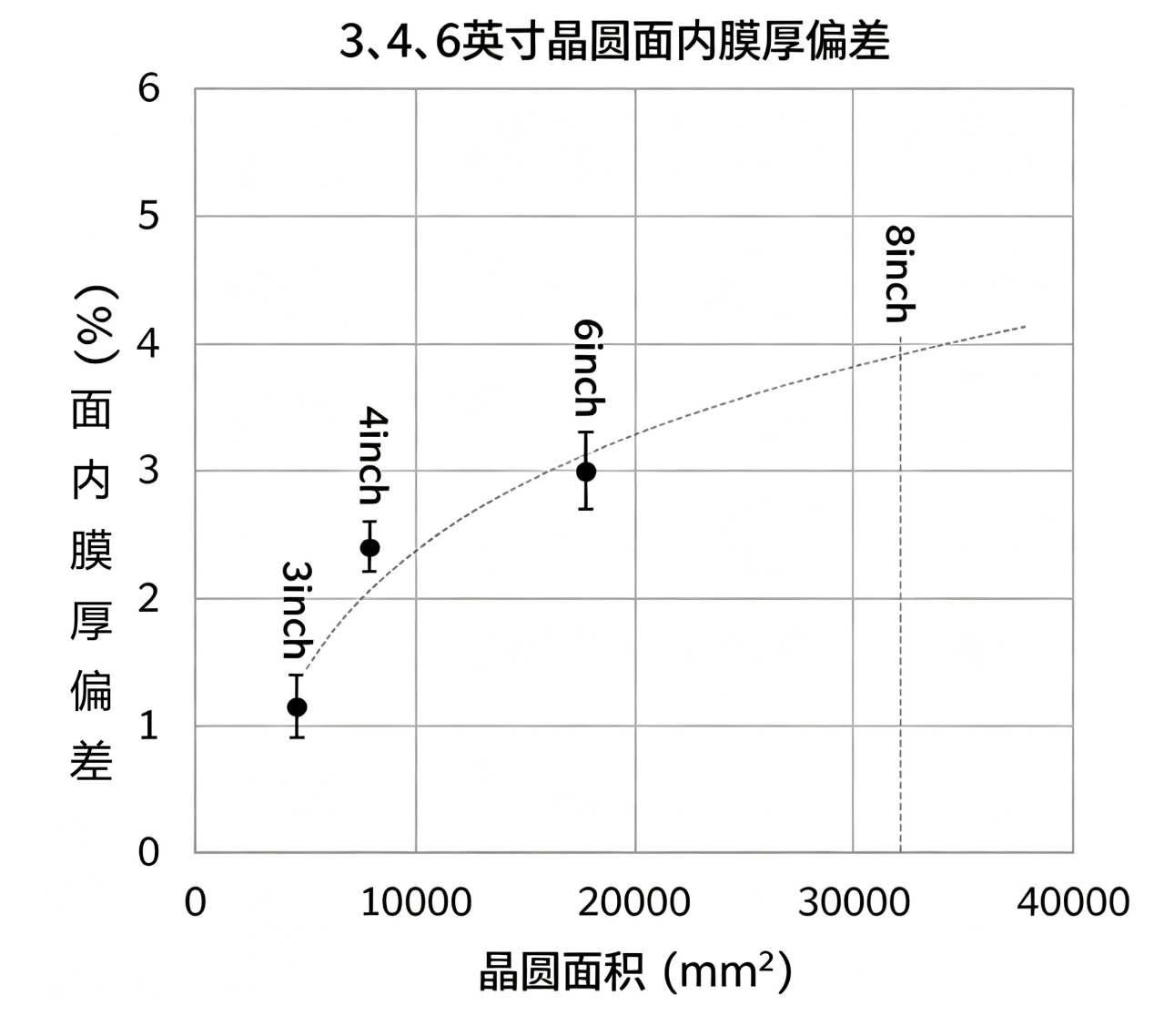
Figure 2. Relationship between wafer area and in-plane film thickness uniformity. The 3-, 4-, and 6-inch data represent experimental measurements; the dashed line indicates the fitted curve, and the 8-inch result is a prediction based on the fitted curve.
Significance: Accelerating Mass Production by Leveraging Existing Production Lines
Compared with a 4-inch wafer, a 6-inch wafer has approximately 2.2 times the surface area, potentially increasing the number of chips obtainable from each wafer by a similar factor. This can reduce the cost per chip not only during epitaxial growth but also throughout the device front-end manufacturing process.
In addition, 6-inch sapphire substrates are widely used in the LED industry, making them available in large volumes at relatively low cost with a stable supply.
Manufacturers of SiC power semiconductors or gallium nitride (GaN) LEDs that already operate 6-inch production lines can potentially use their existing front-end processing equipment to manufacture gallium oxide power semiconductors. This approach could reduce additional capital investment and accelerate the establishment and launch of mass-production lines.
FLOSFIA regards MOSFET performance validation and the scaling up of epitaxial growth as two key pillars for commercializing gallium oxide power semiconductors. The latest achievement demonstrates steady progress in scaling up its epitaxial growth technology.
Future Outlook
FLOSFIA plans to demonstrate epitaxial growth on 8-inch sapphire substrates within 2026. The company will also apply the technical knowledge gained from large-diameter wafer growth to the development of GaO® power devices, including MOSFETs, and to the establishment of mass-production processes with its partners.
In parallel, FLOSFIA aims to expand its partnerships through technology licensing and epitaxial wafer supply, with the goal of accelerating the adoption of its technology in applications such as power supplies for electric vehicles (EVs) and artificial intelligence (AI) data centers.
Acknowledgments
Part of this research was supported by the Acquisition, Technology & Logistics Agency (ATLA) of Japan under the Security Technology Research Promotion Program (JPJ004596).
Kenji Amada, Representative Director and President of FLOSFIA, commented:
“This achievement represents an important step toward enabling our partners to manufacture GaO® power devices using their existing mass-production lines. Building on this milestone, we will accelerate the development of 8-inch wafer technology and the performance validation of MOSFETs, further advancing the commercialization of gallium oxide power semiconductors.”
Instruction
Official Account

Cooperation
Top