


Researchers from University of California Santa Barbara have published a dissertation titled " Cr₂O₃/β-Ga₂O₃ heterojunction diodes with orientation-dependent breakdown electric field " in Applied Physics Letters.
Background
In recent years of wide/ultra-wide bandgap (WBG/UWBG) semiconductor advancements, β-Ga₂O₃ offers promising potential for medium-voltage power applications (1-35 kV) in applications of power conversion at grid scale, renewable energy processing, and data centers for artificial intelligence (AI). The high critical electric field strength and availability of the shallow hydrogenic dopants1 in epitaxial β-Ga₂O₃ can be leveraged to demonstrate power devices with much lower differential specific on-resistance while operating at a higher blocking voltage compared to silicon carbide (SiC) and gallium nitride (GaN). To fully exploit the high electric field advantage of β-Ga₂O₃, integrations with high-dielectric constant (high-κ) oxides were realized to achieve 5.7 MV/cm average electric field at breakdown10. High electric field of 4.3 MV/cm has been reported using oxidized large barrier height β-Ga₂O₃ Schottky barrier diodes (SBDs). Although reliable p-type doping with mobile holes in β-Ga₂O₃ is currently unavailable, p-type oxides, such as nickel oxide (NiO), was integrated with β-Ga₂O₃ to form P-N heterojunctions that readily enable multi-kV junctions with breakdown voltage >10 kV and high electric field at 7.5 MV/cm. Because of the monoclinic asymmetric crystal structure of β-Ga₂O₃, anisotropies in various material parameters are expected, such as relative permittvity, thermal conductivity, and critical electric field. Recently, we have reported crystal orientation-dependence of breakdown electric field between (100) and (001) β-Ga₂O₃ using NiO/β-Ga₂O₃ diodes. Nevertheless, a systematic comparison of breakdown electric field analysis across available crystal orientations of bulk-grown β-Ga₂O₃ needs to be explored.
Abstract
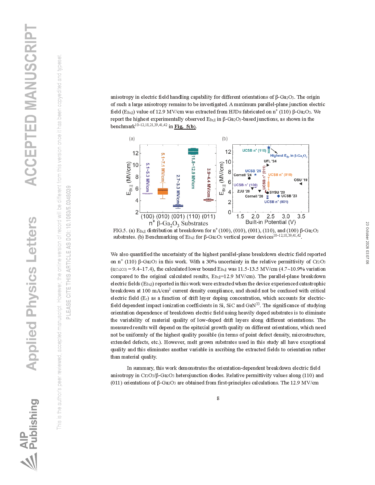
We report the fabrication of Cr₂O₃/β-Ga₂O₃ heterojunction diodes using reactive magnetron sputtering of Cr₂O₃ on highly doped β-Ga₂O₃ bulk substrates along (100), (010), (001), (110), and (011) orientation dependence of high electric field handling capability in β Ga₂O₃. Additional relative permittivity values in (110) and (011) orientations of β-Ga₂O₃ were computed by using first-principles calculation methods for accurate apparent charge density (ND NA) extraction and breakdown electric field analysis from capacitance-voltage measurements. The HJDs fabricated on n⁺ (110) exhibited breakdown electric fields >10 MV/cm up to 12.9 MV/cm, showing the highest experimentally observed parallel-plane junction electric field among β-Ga₂O₃-based junctions. Breakdown electric fields among (100), (010), (001), and (011) orientations showed distinct distribution in the range of 5.13-5.26 MV/cm, 5.10-7.05 MV/cm, 2.70-3.33 MV/cm, and 3.88-4.38 MV/cm, respectively, validating the orientational dependence of parallel-plane junction electric field at breakdown in low-symmetry monoclinic β-Ga₂O₃. The parallel-plane breakdown electric fields (EBr,||) reported in this work were extracted when the device experienced catastrophic breakdown at 100 mA/cm² current density compliance, and should not be confused with critical electric field (Ec) as a function of drift layer doping concentration, which accounts for electric-field dependent impact ionization coefficients in Si, SiC and GaN. This study can guide the choice of crystal orientation for high-performance gallium oxide-based devices that require high electric field handling capability.
Highlights
System preparation and anisotropy verification of polycrystalline heterojunctions: Researchers successfully prepared Cr₂O₃/β-Ga₂O₃heterojunction diodes (HJDs) on five different crystal orientations ((100), (010), (001), (110), and (011)) of β-Ga₂O₃ bulk substrates using reactive magnetron sputtering technology, systematically verifying the strong anisotropy distribution of breakdown electric field in low-symmetry monoclinic crystals.
First-principles calculations to complete key dielectric constants: Based on density functional perturbation theory (DFPT), the relative dielectric constants of β-Ga₂O₃along (110) and (011) crystal directions were calculated and obtained, laying a solid foundation for accurately extracting apparent carrier concentration and analyzing the breakdown electric field of various crystal directions.
Record-breaking ultra-high parallel plane breakdown electric field: Experiments have shown that the heterojunction diode fabricated on the n⁺(110) crystal orientation achieves a parallel plane breakdown electric field exceeding 10 MV/cm, with a peak value of 12.9 MV/cm, setting a new record for the highest parallel plane junction electric field experimentally observed in β-Ga₂O₃-based junction devices to date.
Clarify the guiding significance of crystal orientation selection for device performance: By evaluating the breakdown electric field of various crystal orientations on heavily doped substrates, the interference from quality differences in low-doped drift layer materials is eliminated, providing an important basis for crystal orientation selection in the future design and optimization of gallium oxide power devices with high voltage resistance and high electric field withstand capability.
Conclusion
In summary, this work demonstrates the orientation-dependent breakdown electric field anisotropy in Cr₂O₃/β-Ga₂O₃ heterojunction diodes. Relative permittivity values along (110) and (011) orientations of β-Ga₂O₃ are obtained from first-principles calculations. The 12.9 MV/cm parallel-plane breakdown electric field obtained on (110) β-Ga₂O₃ exhibits the highest experimentally observed breakdown electric field among β-Ga₂O₃-based junctions across literatures.
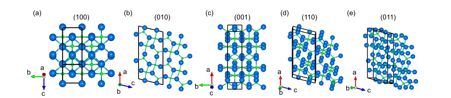
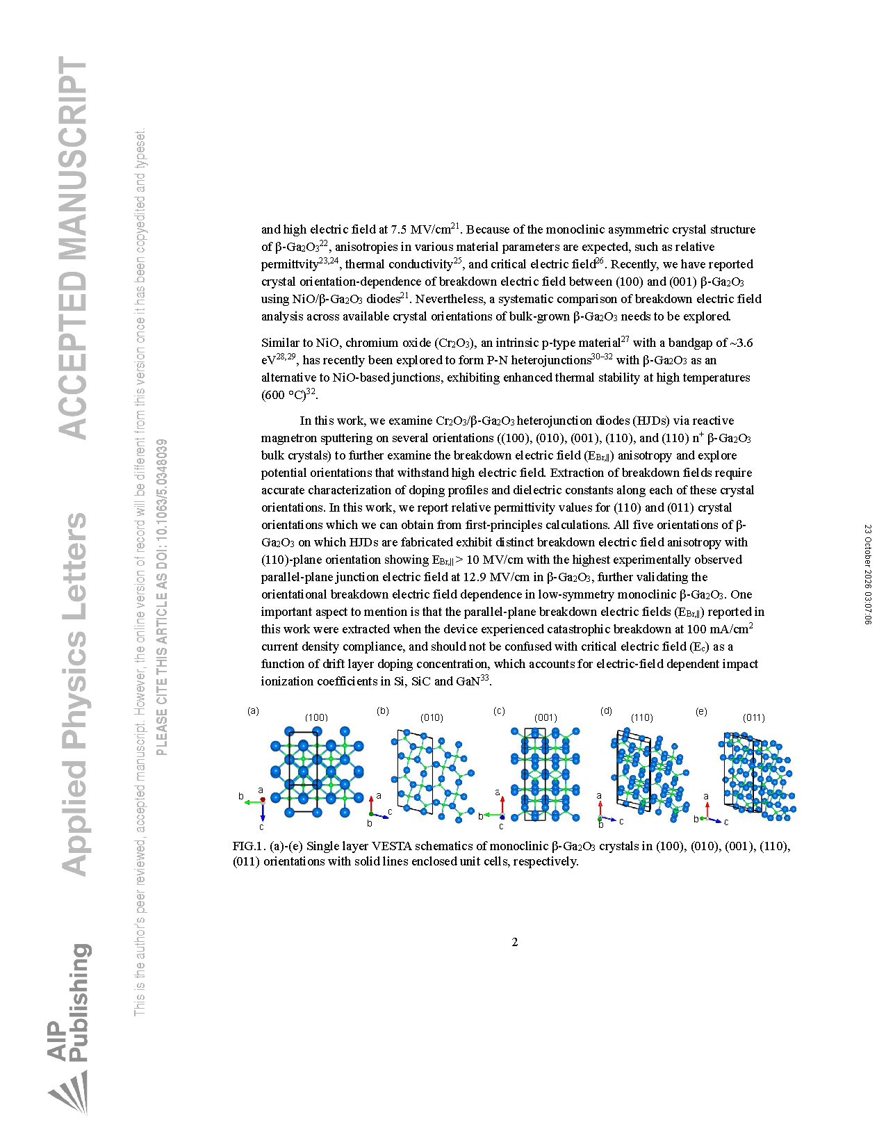
FIG.1. (a)-(e) Single layer VESTA schematics of monoclinic β-Ga₂O₃ crystals in (100), (010), (001), (110), (011) orientations with solid lines enclosed unit cells, respectively.
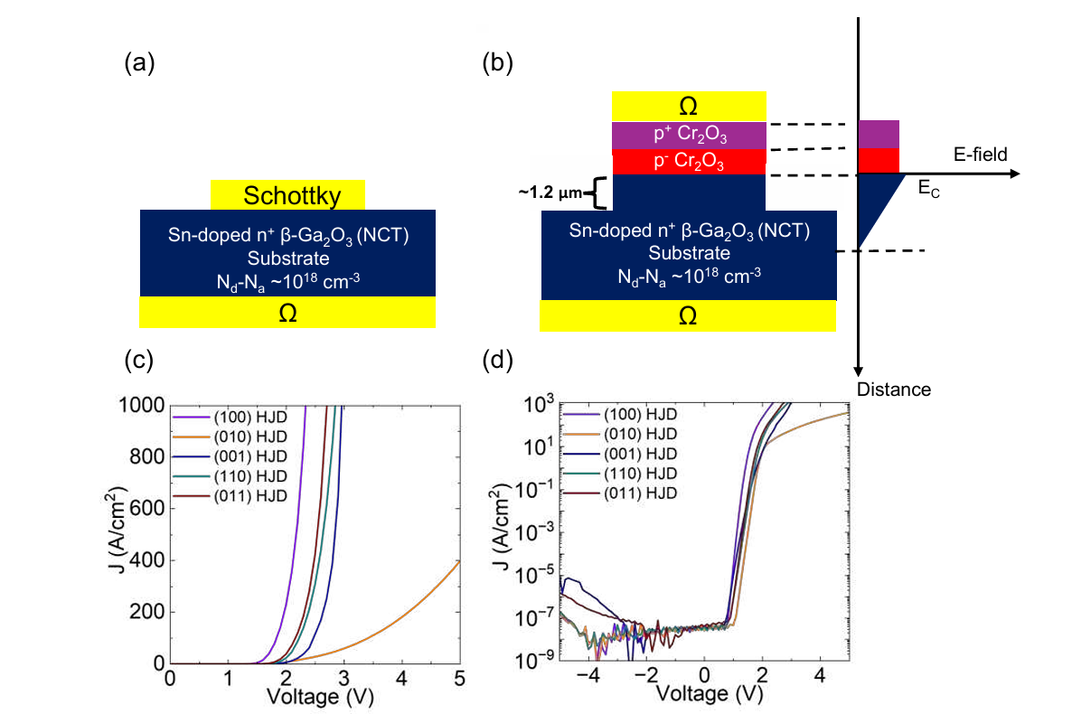
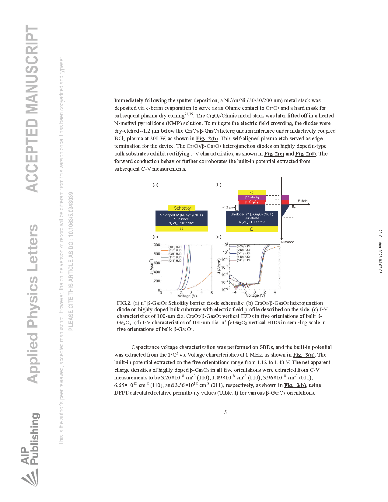
FIG.2. (a) n⁺ β-Ga₂O₃ Schottky barrier diode schematic. (b) Cr₂O₃/β-Ga₂O₃ heterojunction diode on highly doped bulk substrate with electric field profile described on the side. (c) J-V characteristics of 100-μm dia. Cr₂O₃/β-Ga₂O₃ vertical HJDs in five orientations of bulk β Ga₂O₃. (d) J-V characteristics of 100-μm dia. n⁺ β-Ga₂O₃ vertical HJDs in semi-log scale in five orientations of bulk β-Ga₂O₃.
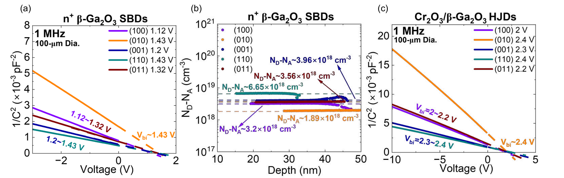
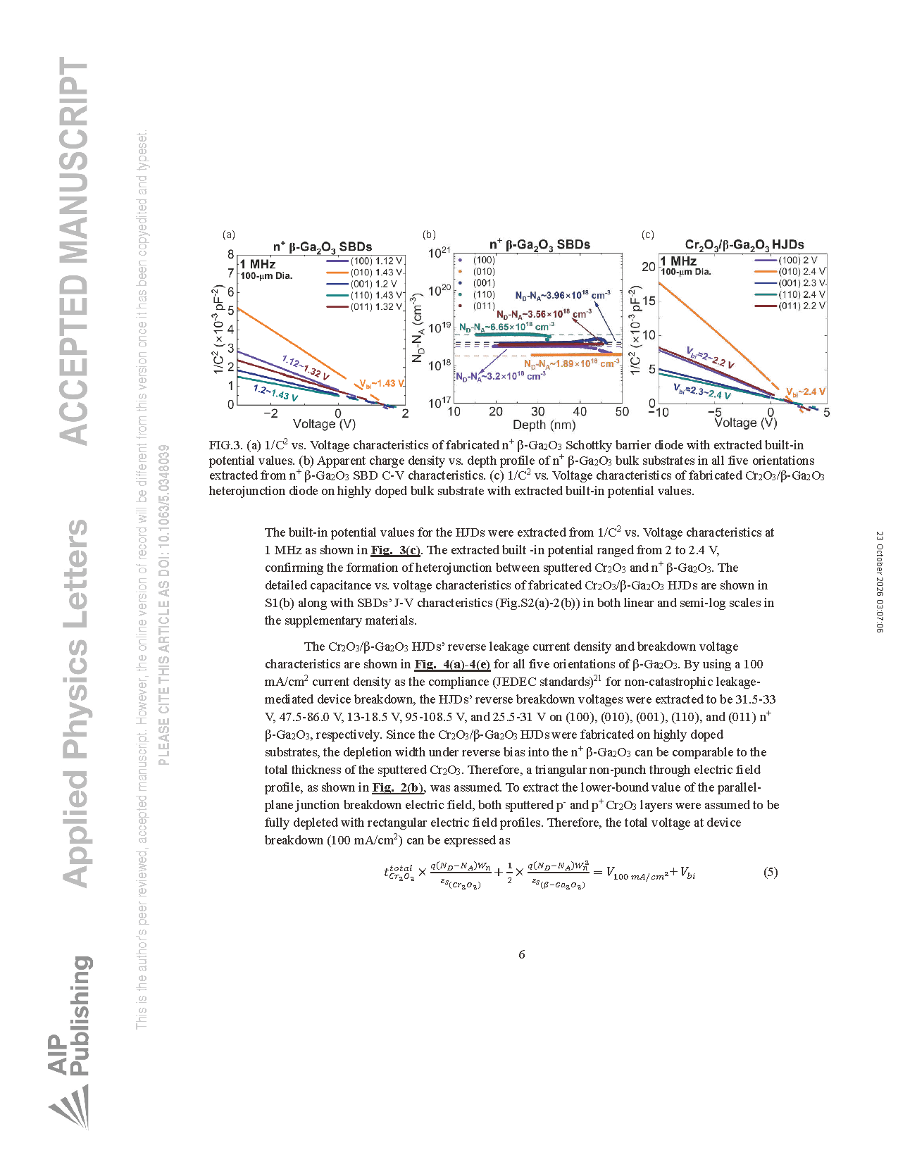
FIG.3. (a) 1/C² vs. Voltage characteristics of fabricated n⁺ β-Ga₂O₃ Schottky barrier diode with extracted built-in potential values. (b) Apparent charge density vs. depth profile of n⁺ β-Ga₂O₃ bulk substrates in all five orientations extracted from n⁺ β-Ga₂O₃ SBD C-V characteristics. (c) 1/C² vs. Voltage characteristics of fabricated Cr₂O₃/β-Ga₂O₃ heterojunction diode on highly doped bulk substrate with extracted built-in potential values.
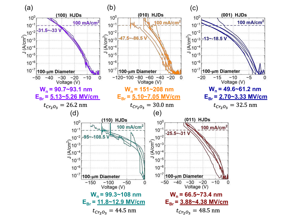
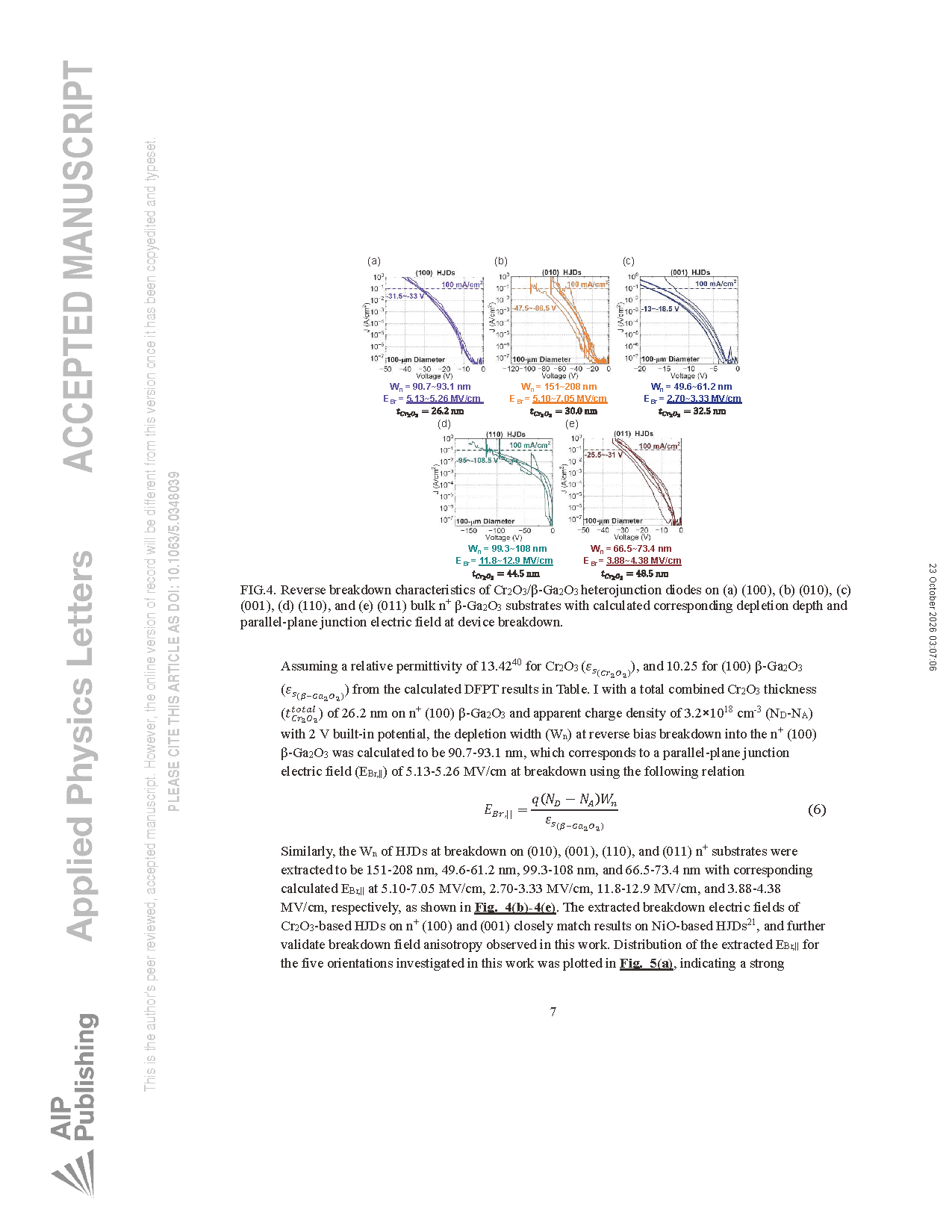
FIG.4. Reverse breakdown characteristics of Cr₂O₃/β-Ga₂O₃ heterojunction diodes on (a) (100), (b) (010), (c) (001), (d) (110), and (e) (011) bulk n⁺ β-Ga₂O₃ substrates with calculated corresponding depletion depth and parallel-plane junction electric field at device breakdown.
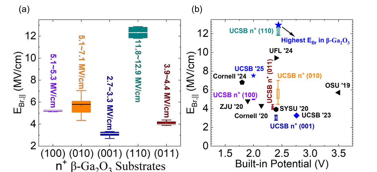
FIG.5. (a) EBr,|| distribution at breakdown for n⁺ (100), (010), (001), (110), and (100) β-Ga₂O₃ substrates. (b) Benchmarking of EBr,|| for β-Ga₂O₃ vertical power devices.
DOI:
doi.org/10.1063/5.0348039

Instruction
Official Account

Cooperation
Top
