


Researchers from Xi'an Jiaotong University and Xidian University have published a dissertation titled " Elucidating oxygen vacancy passivation mechanism at Al₂O₃/β-Ga₂O₃ interface via supercritical N₂O processing " in Applied Physics Letters.
Background
β-Ga₂O₃ has a bandgap of approximately 4.8eV and a predicted breakdown field above 8 MV cm−1, making it attractive for high-voltage power devices. Atomic-layer-deposited (ALD) Al₂O₃ is widely used as the gate dielectric because of its favorable conduction-band offset and process compatibility. However, Al₂O₃/β-Ga₂O₃ interfaces commonly exhibit interface-trap densities (Dit) of 1012–1013cm−2eV−1, which contribute to threshold-voltage drift and gate leakage. Spectroscopic and first-principles studies have linked part of this trap population to surface oxygen vacancies (VO) and their associated in-gap states.
Abstract
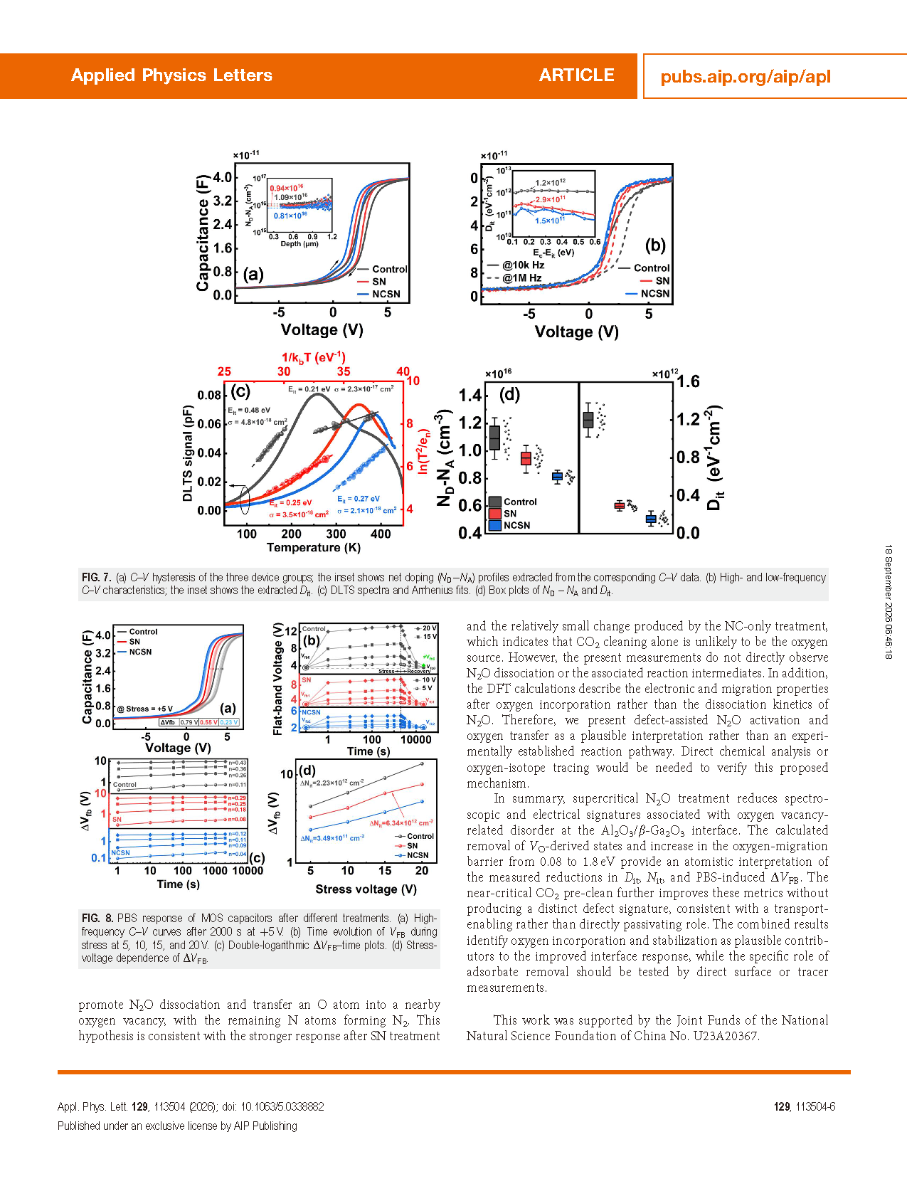
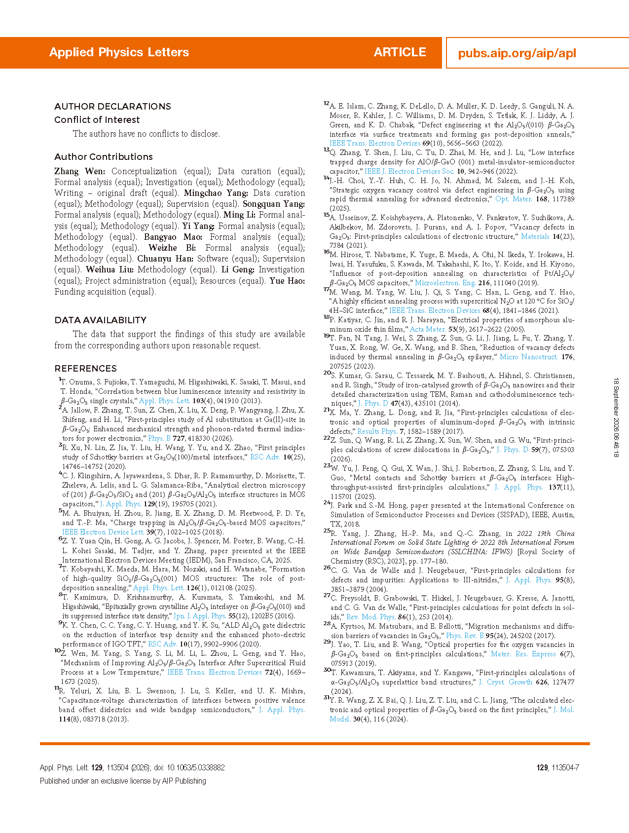
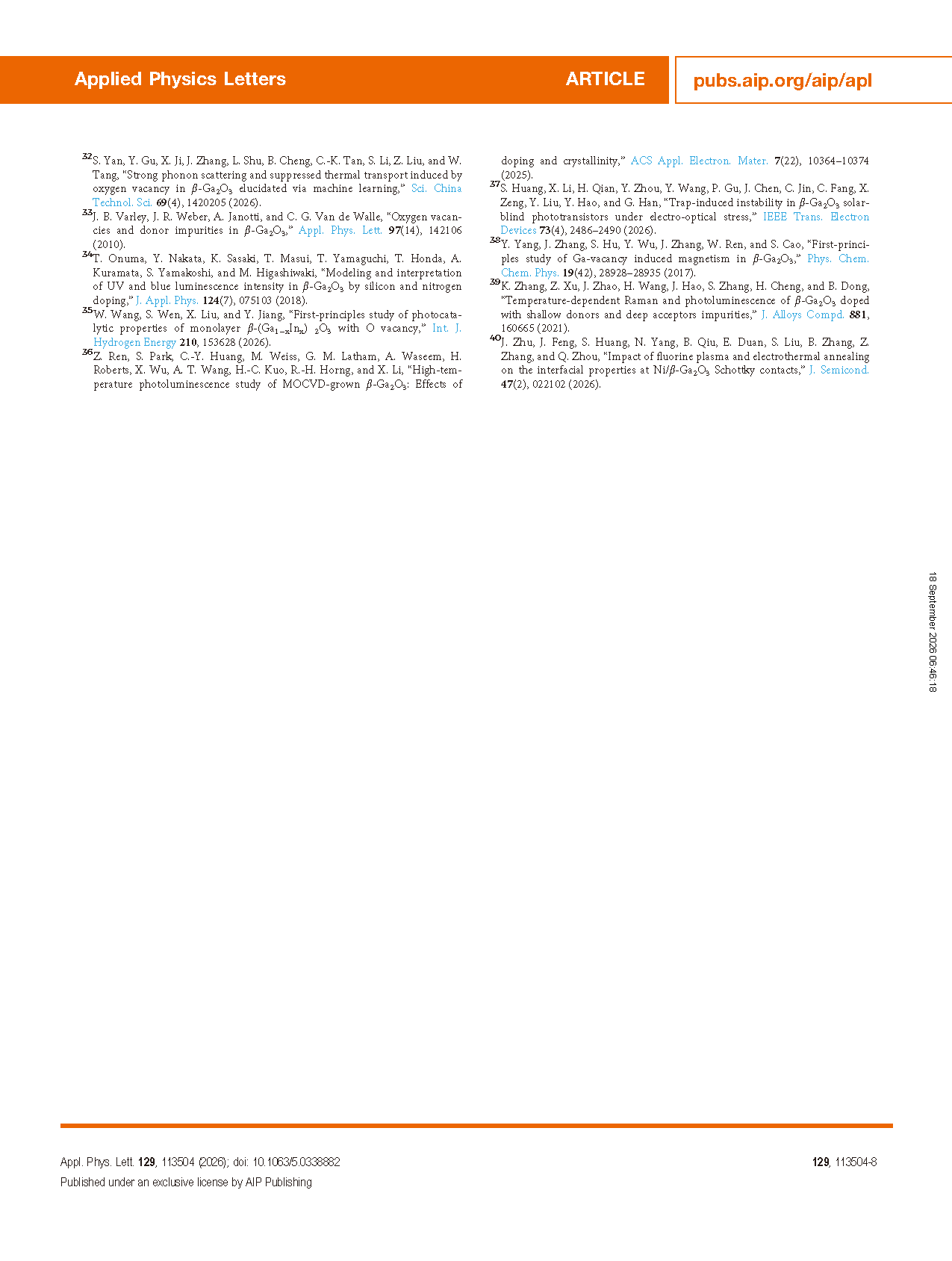
Oxygen vacancies (VO) at the β-Ga₂O₃ surface are associated with the high interface-trap densities (Dit, 1012–1013 cm−2 eV−1) that limit the threshold-voltage stability in Al₂O₃/β-Ga₂O₃ MOS devices. We combine first-principles calculations with Raman spectroscopy, photoluminescence (PL), x-ray photoelectron spectroscopy, and electrical characterization to examine how supercritical-fluid processing modifies these interface states. Perdew–Burke–Ernzerhof calculations with a rigid scissor correction to the experimental 4.8 eV bandgap identify in-gap states associated with the three inequivalent VO sites. Interstitial oxygen removes these states in the calculated model and increases the migration barrier from 0.08 to 1.8 eV. Experimentally, supercritical N₂O (SN) treatment narrows the Raman linewidths at 347, 416, and 767 cm−1, suppresses the 2.4 and 2.8 eV defect-related PL bands, and increases the lattice-oxygen fraction from approximately 50% to more than 80%. A near-critical CO2 pre-clean further improves the SN response, consistent with removal of surface adsorbates before oxidation. The resulting NCSN process reduces Dit to 1.5 × 1011 cm−2 eV−1, lowers Nit by a factor of 6.4, and decreases the positive-bias-stress flatband-voltage shift from 0.79 to 0.23 V. Together, the calculations and measurements support oxygen vacancy filling and reduced oxygen migration as the main contributors to interface passivation.
Conclusion
In summary, supercritical N₂O treatment reduces spectroscopic and electrical signatures associated with oxygen vacancy-related disorder at the Al₂O₃/β-Ga₂O₃ interface. The calculated removal of VO-derived states and increase in the oxygen-migration barrier from 0.08 to 1.8 eV provide an atomistic interpretation of the measured reductions in Dit, Nit, and PBS-induced ΔVFB. The near-critical CO2 pre-clean further improves these metrics without producing a distinct defect signature, consistent with a transport- enabling rather than directly passivating role. The combined results identify oxygen incorporation and stabilization as plausible contributors to the improved interface response, while the specific role of adsorbate removal should be tested by direct surface or tracer measurements.
Project Support
This work was supported by the Joint Funds of the National Natural Science Foundation of China No. U23A20367.
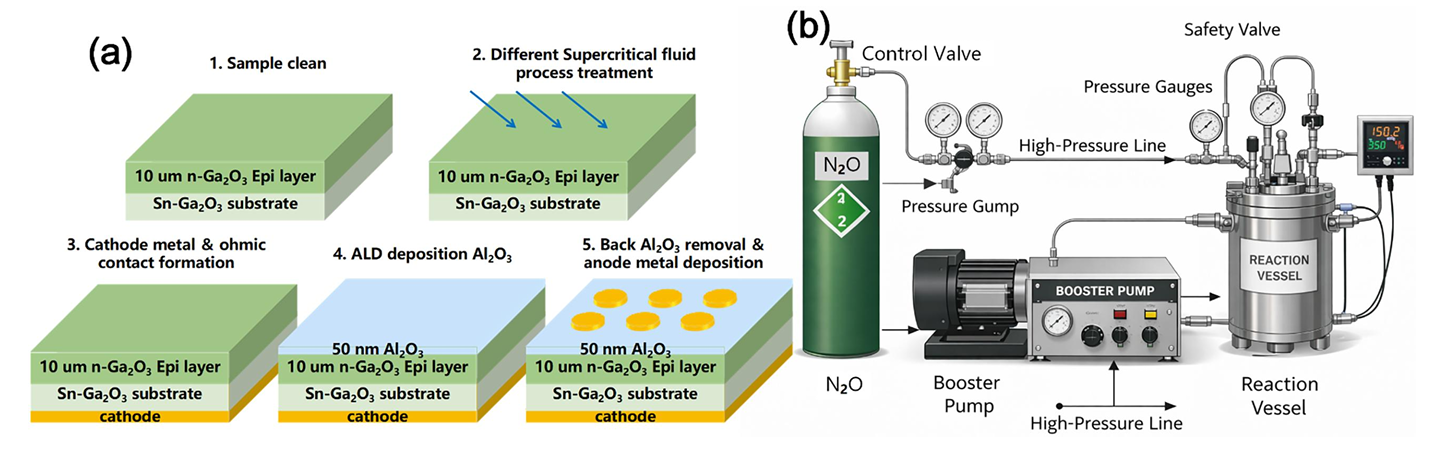
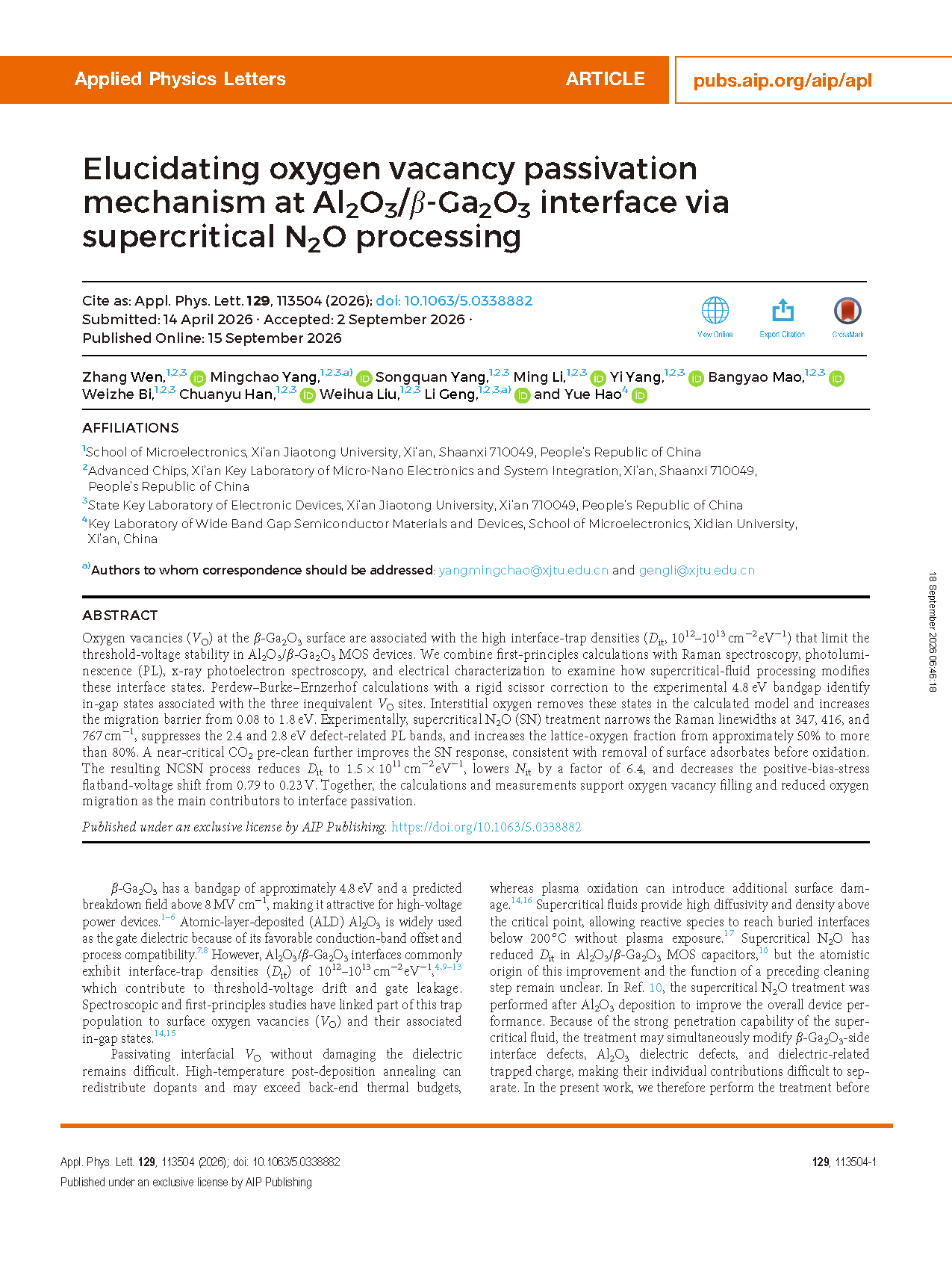
FIG. 1. (a) Schematic of device fabrication process and (b) supercritical-fluid processing system.
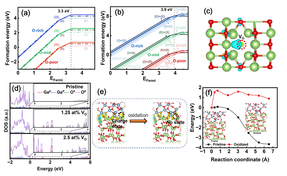
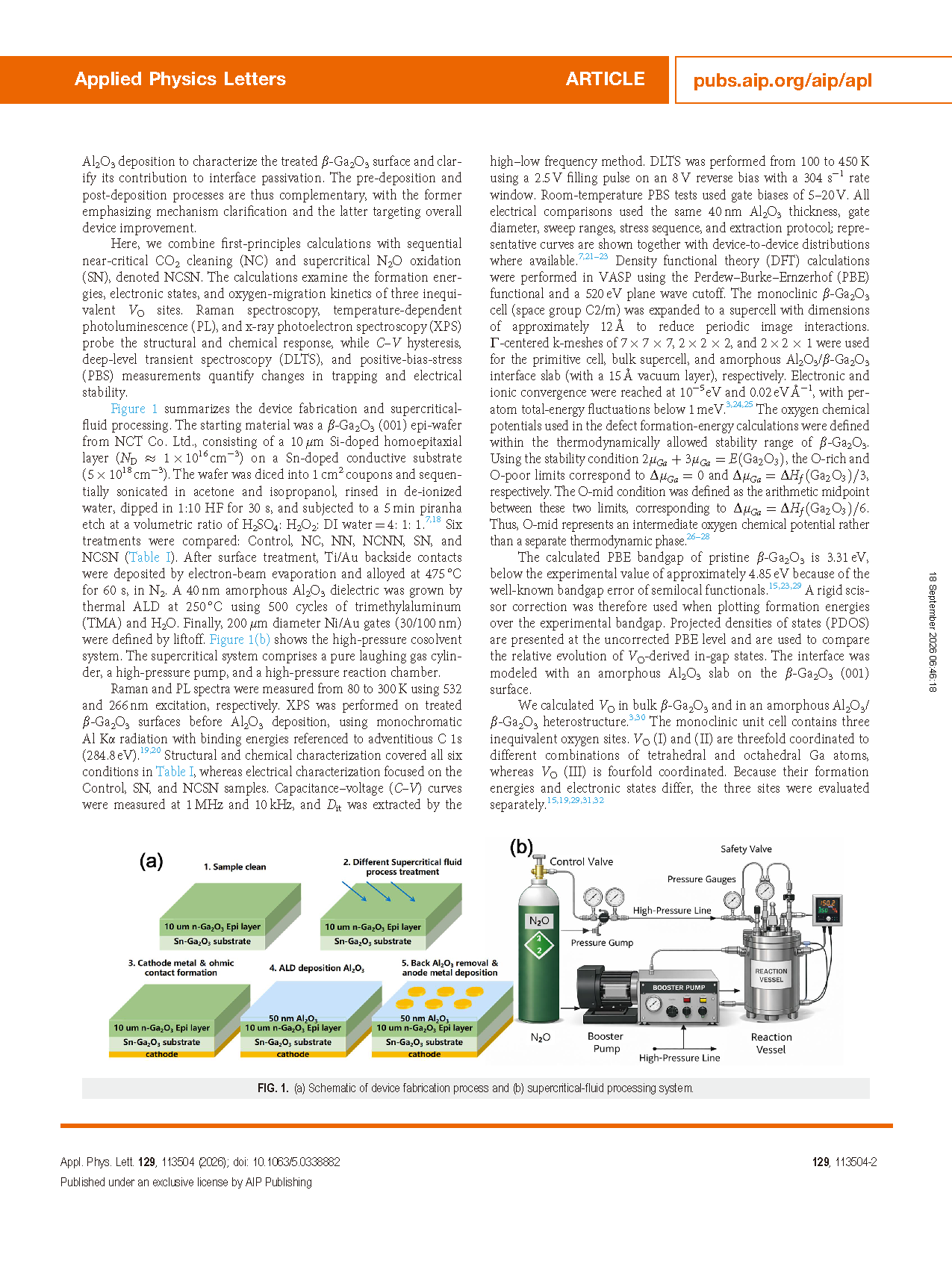
FIG. 2. (a) Formation energy of a single oxygen vacancy as a function of Fermi level over the scissor-corrected 0–4.8eV range and (b) corresponding results for a divacancy. (c) Charge-density difference upon VO ionization (yellow: accumulation; blue: depletion). (d) PDOS for pristine, 1.25at. %, and 2.5at. % VO concentrations, the reported bandgap values (3.31, 1.87, and 1.63eV) are uncorrected PBE values. (e) Charge-density difference before and after oxygen insertion. (f) Migration energy barriers for interface oxygen atoms; inset: migration pathway. The labels “O-rich,” “O-mid,” and “O-poor” refer to the oxygen chemical-potential conditions defined above.
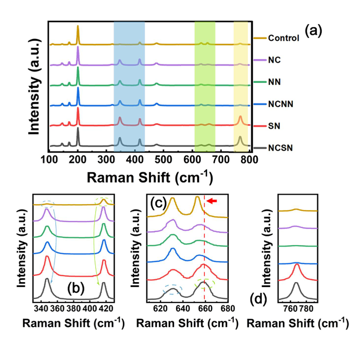
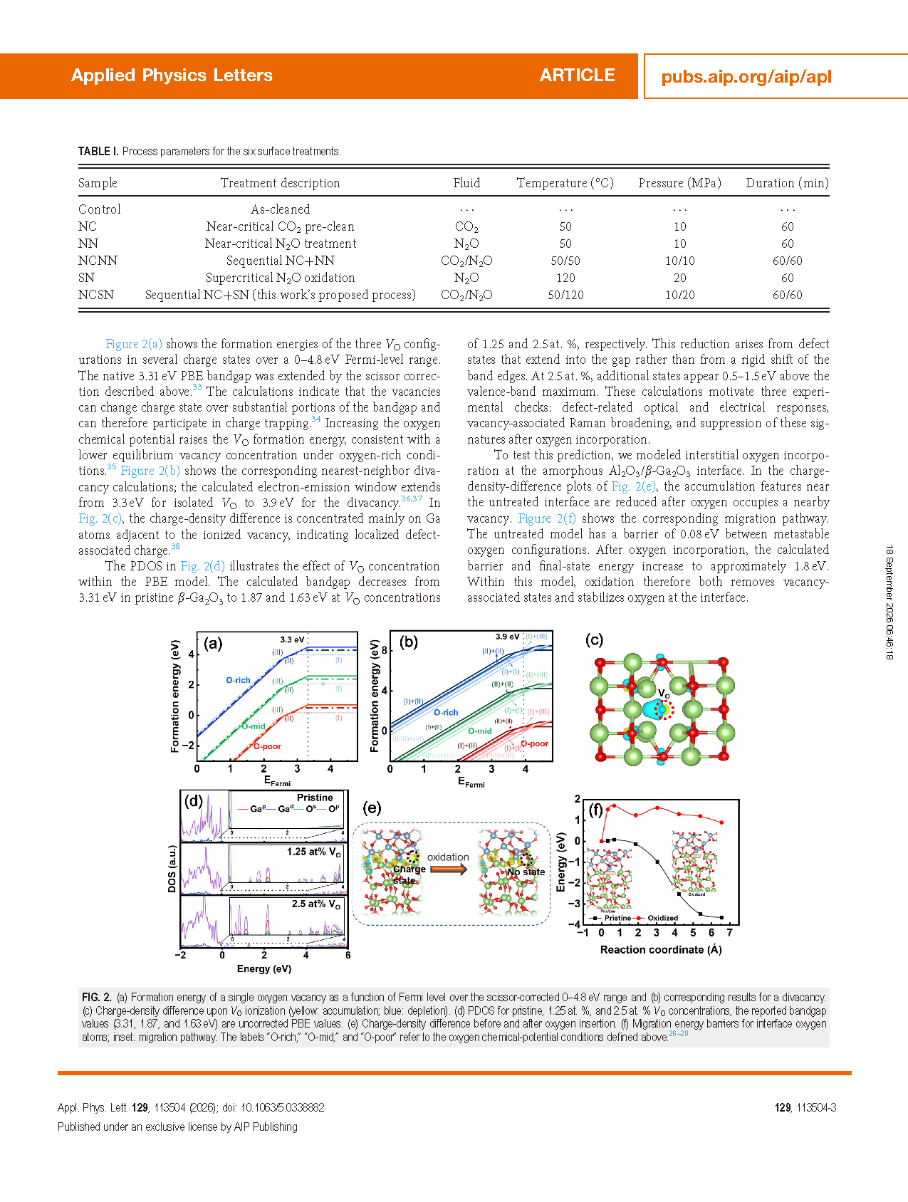
FIG. 3. (a) Room-temperature Raman spectra of Ga₂O₃ after different fluid treatments. (b)–(d) Enlarged spectra over 335–425, 610–680, and 750–790cm−1.
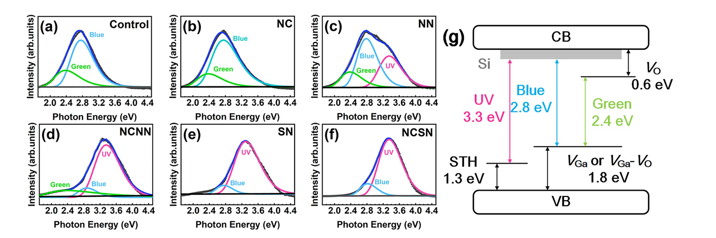
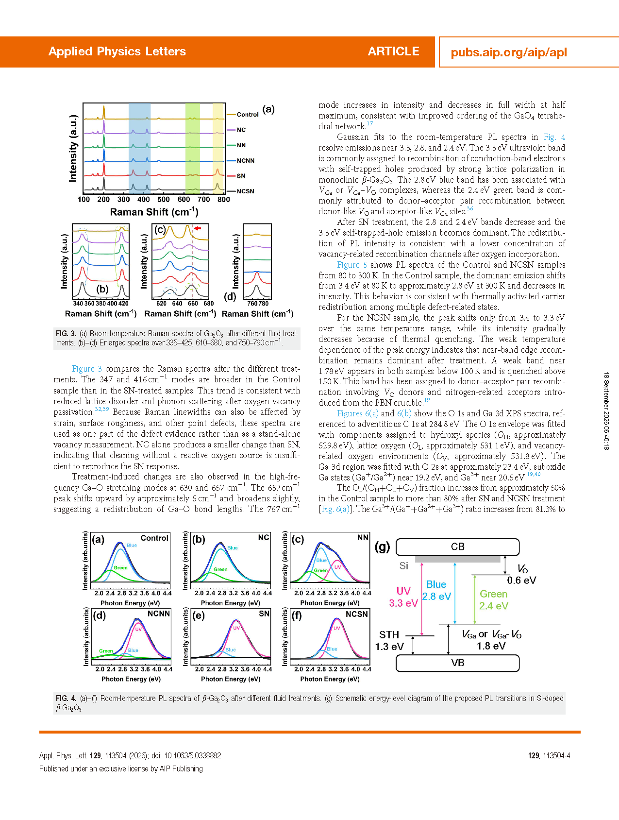
FIG. 4. (a)–(f) Room-temperature PL spectra of β-Ga₂O₃ after different fluid treatments. (g) Schematic energy-level diagram of the proposed PL transitions in Si-doped β-Ga₂O₃.
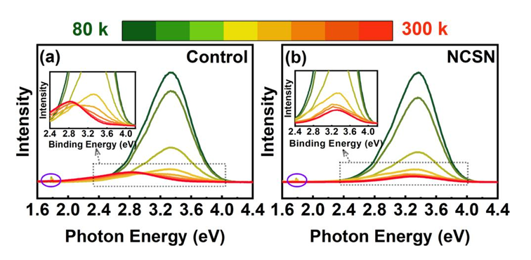
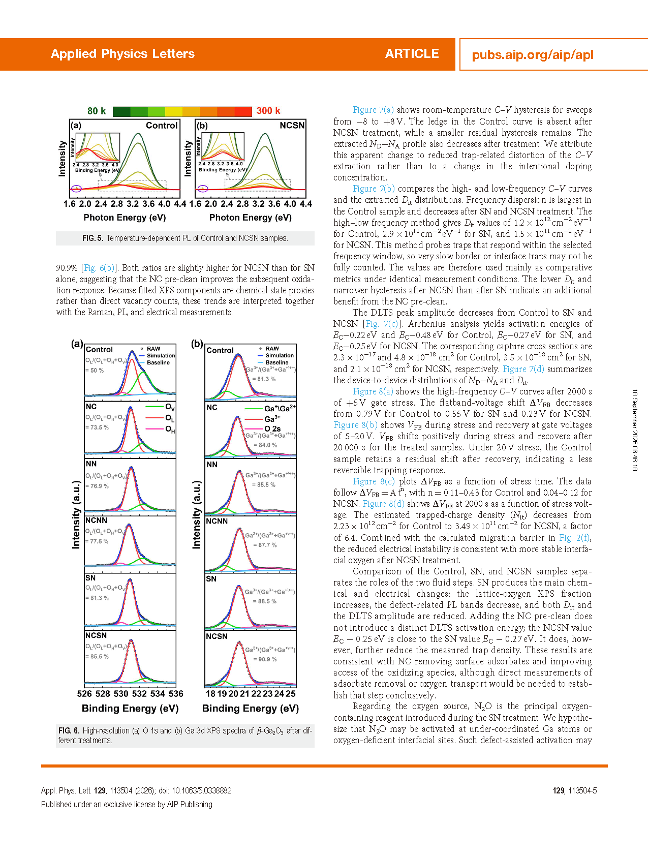
FIG. 5. Temperature-dependent PL of Control and NCSN samples.
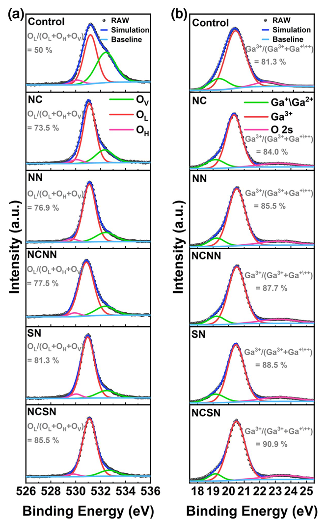
FIG. 6. High-resolution (a) O 1s and (b) Ga 3d XPS spectra of β-Ga₂O₃ after different treatments.
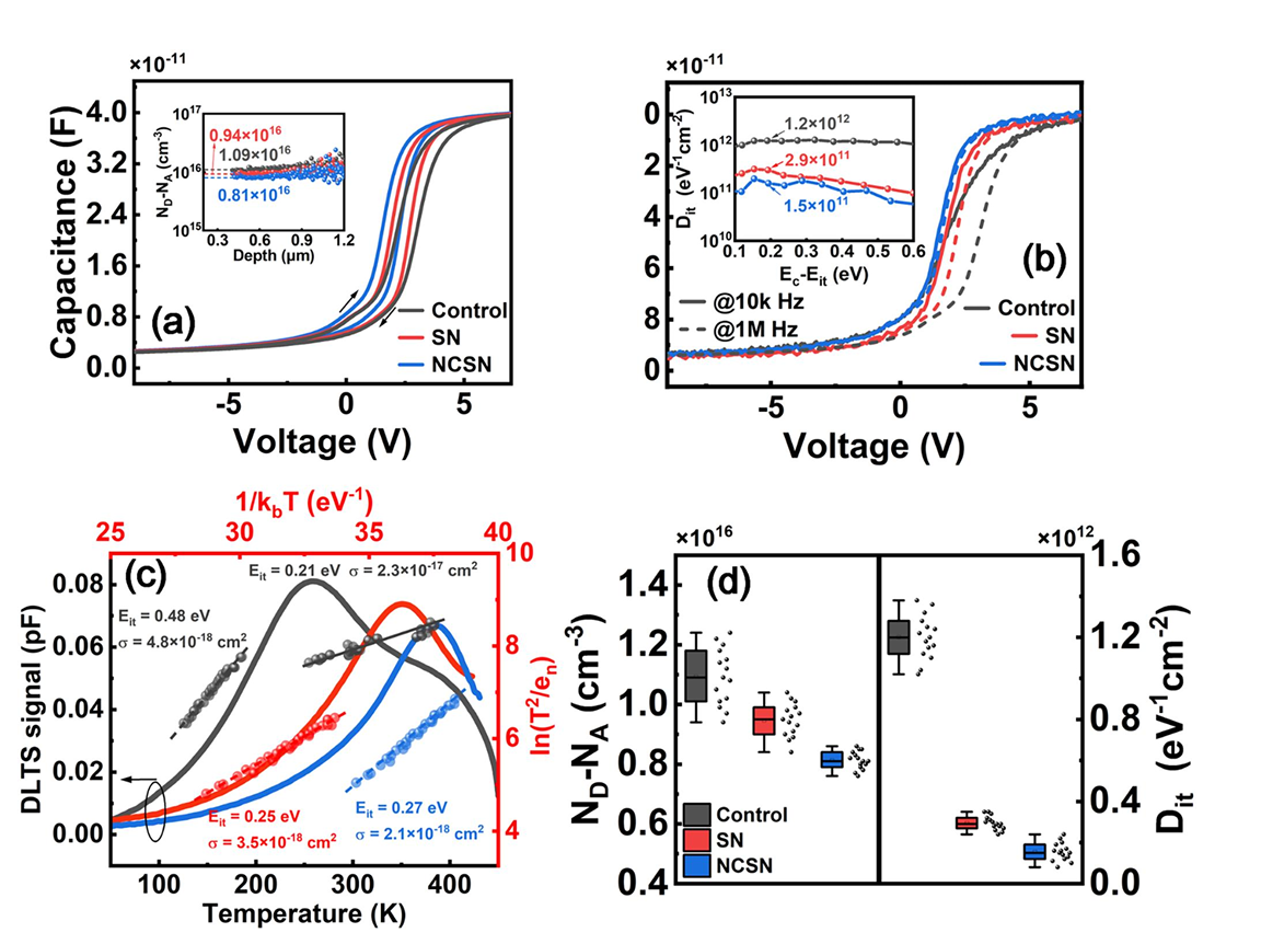
FIG. 7. (a) C–V hysteresis of the three device groups; the inset shows net doping (ND−NA) profiles extracted from the corresponding C–V data. (b) High- and low-frequency C–V characteristics; the inset shows the extracted Dit. (c) DLTS spectra and Arrhenius fits. (d) Box plots of ND– NA and Dit.
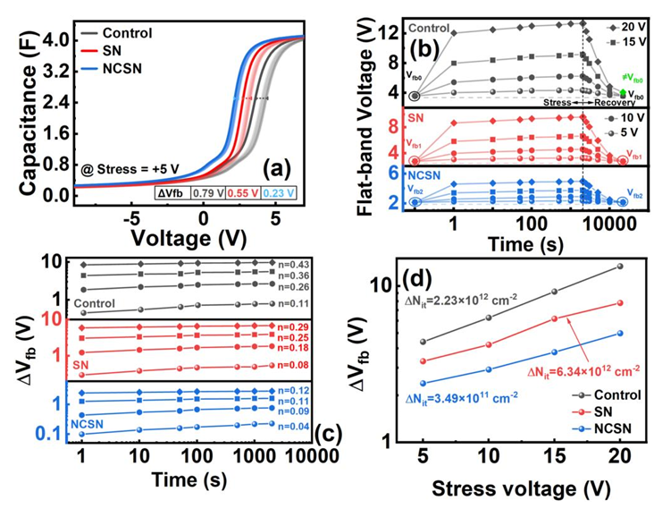
FIG. 8. PBS response of MOS capacitors after different treatments. (a) High- frequency C–V curves after 2000 s at +5 V. (b) Time evolution of VFB during stress at 5,10,15,and 20 V. (c) Double-logarithmic ΔVFB-time plots. (d)Stress-voltage dependence of ΔVFB.
DOI:
doi.org/10.1063/5.0338882
Instruction
Official Account

Cooperation
Top
