


A paper by Professor Weifeng Yang’s team at Xiamen University, published in the journal Applied Physics Letters, is titled “Competing Self-Trapped Hole Release and Deep-Level Defect Recombination in Ga2O3 Photodetectors.” Using plasma-assisted molecular beam epitaxy (PAMBE), the team prepared (-201)- and (400)-oriented β-Ga2O3 thin films on sapphire and 4H-SiC substrates, respectively. The crystal quality and defect characteristics of the two films were systematically compared, and the temperature-dependent photoresponse performance of photodetectors based on the two films was systematically investigated. It was found that the (-201)-β-Ga2O3 film had a sharp interface and a lower defect density, and its photodetector exhibited nonmonotonic photocurrent behavior originating from the thermally activated release of self-trapped holes. In contrast, owing to an amorphous SiOx interfacial layer, the (400)-β-Ga2O3 film had higher densities of dislocations and oxygen vacancies; deep-level defect recombination centers effectively suppressed the contribution of self-trapped holes, leading to a monotonic decrease in photocurrent and, simultaneously, a faster response speed. This work reveals a competing mechanism between self-trapped hole release and deep-level defect recombination, providing an important reference for optimizing the performance of β-Ga2O3 solar-blind photodetectors through substrate and orientation engineering.
Background
Gallium oxide, as an ultra-wide-bandgap semiconductor material, exhibits a bandgap of approximately 4.5-4.9 eV, a critical breakdown field strength as high as 8 MV/cm, and a Baliga figure of merit approaching 3000, demonstrating significant application potential in high-voltage power electronics and deep-ultraviolet optoelectronic devices. However, the performance of its photodetectors is significantly affected by defects. Point defects and dislocations introduce localized energy levels within the bandgap, thereby governing carrier dynamics and temperature-dependent photoresponse behavior. Among these, the H1 level associated with self-trapped holes (STHs) can be thermally excited with an activation energy of approximately 0.2 eV, releasing mobile holes that contribute to the photocurrent, whereas deep-level defects such as E2 and H3 serve as nonradiative recombination centers and influence carrier transport behavior. Nevertheless, systematic understanding of the defect differences among differently oriented β-Ga2O3 films and their effects on detection performance is still lacking. Therefore, understanding the competing relationship between self-trapped hole release and deep-level defect recombination, and establishing the correlation among orientation, defects, and photoresponse, constitute an important point of departure for this study.
Abstract
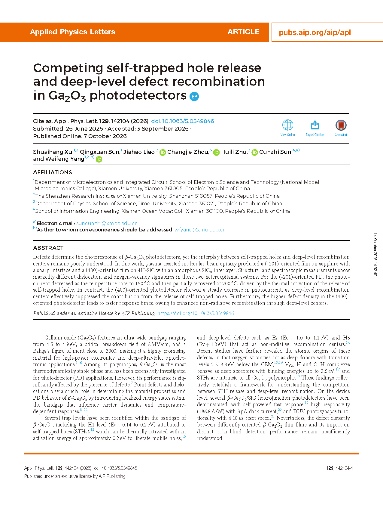
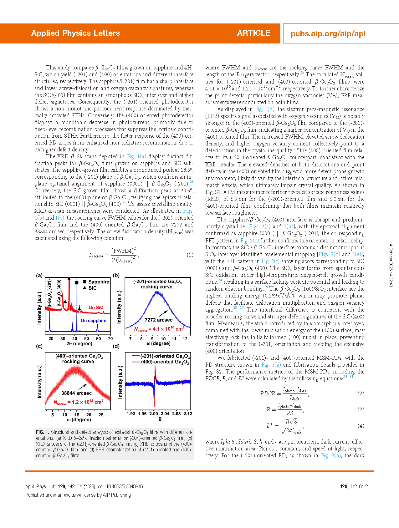
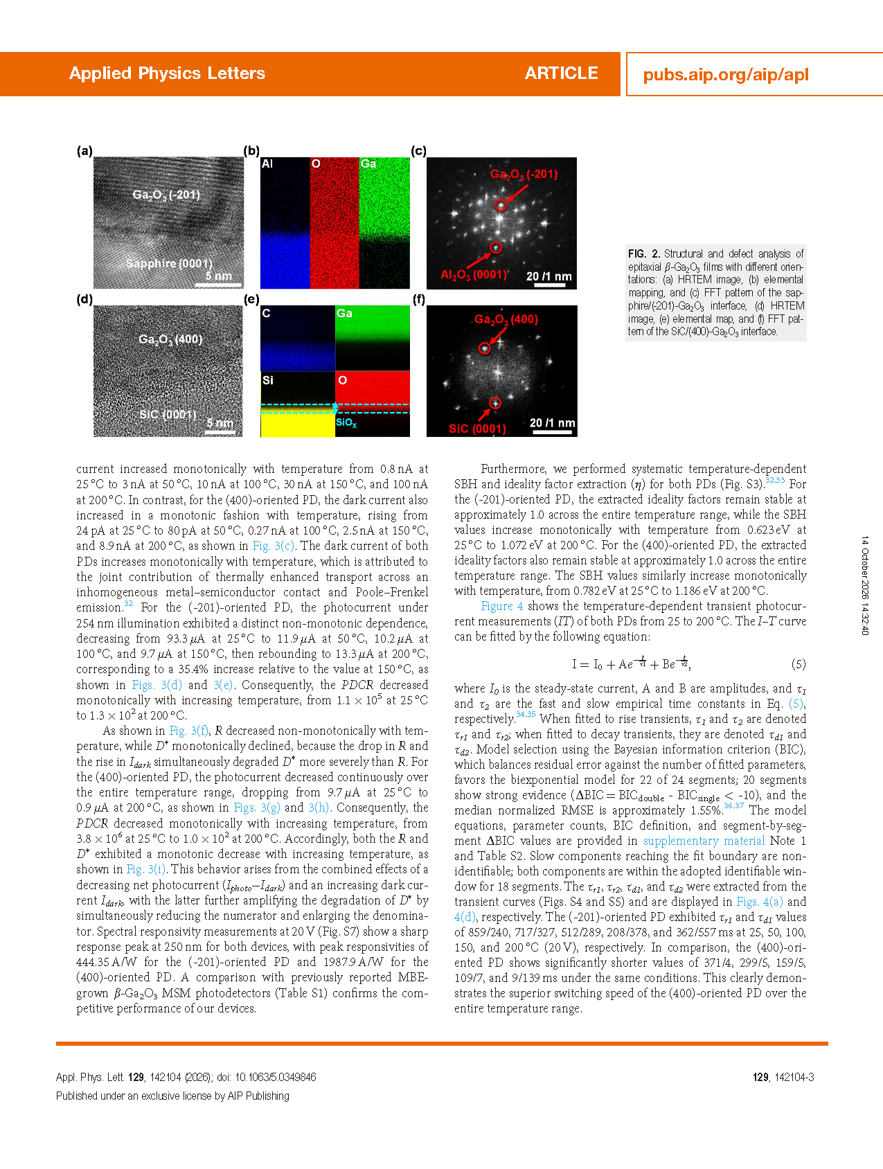
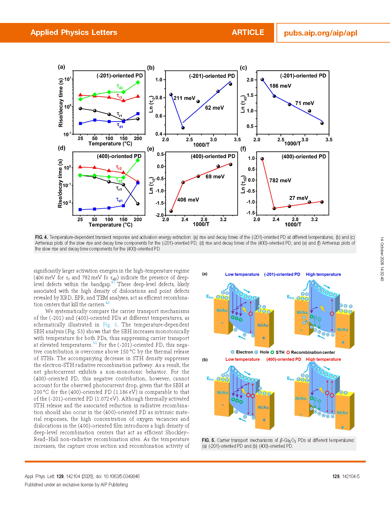
This study adopted a PAMBE strategy to achieve the epitaxial growth of (-201)-oriented and (400)-oriented β-Ga2O3 thin films on sapphire and 4H-SiC substrates, respectively. Through systematic characterization of the heterointerface structures, defect characteristics, and carrier dynamics, it was found that the sapphire-based film formed an atomically sharp Ga2O3/sapphire interface, whereas the SiC-based film possessed an amorphous SiOx interfacial layer; the two exhibited significant differences in screw dislocation density and oxygen vacancy concentration. Experimental results showed that the (-201)-oriented film had a screw dislocation density of 4.11 × 1010 cm-2 and a weak oxygen-vacancy EPR signal, while the (400)-oriented film had a screw dislocation density as high as 1.21 × 1012 cm-2 and a significantly enhanced oxygen-vacancy signal. For the corresponding devices, the photocurrent of the (-201)-oriented photodetector under 254 nm illumination varied nonmonotonically with temperature, decreasing from 93.3 μA at 25 °C to 9.7 μA at 150 °C and then recovering to 13.3 μA at 200 °C; in contrast, that of the (400)-oriented photodetector exhibited a monotonic downward trend. Furthermore, by combining temperature-dependent transient photocurrent measurements with Arrhenius analysis, the research team extracted the activation energies of the slow-response component. For the (-201)-oriented device, the activation energies in the high-temperature regime were 211 meV (rise) and 186 meV (decay), attributed to the thermal release of self-trapped holes; for the (400)-oriented device, the activation energies in the high-temperature regime were as high as 406 meV and 782 meV, revealing the dominant role of deep-level defect recombination centers in carrier behavior. These results provide an experimental basis for understanding the competing mechanism between self-trapped hole release and deep-level defect recombination in β-Ga2O3 photodetectors.
Highlights
Orientation-controlled epitaxy and interface construction: Through an orientation-controlled heteroepitaxial strategy for gallium oxide, controllable growth of (-201)-oriented and (400)-oriented thin films was successfully achieved, forming two distinctly different crystalline interfaces.
Regulation of defect configurations by orientation: The (-201)-oriented film exhibited a lower screw dislocation density and fewer oxygen vacancies, whereas the (400)-oriented film had a defect density approximately two orders of magnitude higher, revealing a strong correlation between orientation and defect configuration.
Mechanistic competition in temperature-dependent photoresponse: As the temperature increased, the (-201)-oriented photodetector exhibited nonmonotonic photocurrent behavior due to self-trapped hole release (decreasing and then recovering by 35.4% at 200 °C), while the (400)-oriented photodetector was dominated by deep-level defect recombination and showed a continuous monotonic decrease.
Defect-mediated fast switching characteristics: The (400)-oriented photodetector achieved a significantly faster response at 200 °C, with a rise time τr1 = 9 ms and a decay time τd1 = 139 ms, far superior to those of the (-201)-oriented device (τr1 = 362 ms and τd1 = 557 ms), which is attributed to abundant deep-level defects acting as recombination centers that greatly shorten the carrier lifetime.
Conclusion
In this study, through an orientation-controlled epitaxial strategy, controllable growth of (-201)- and (400)-oriented β-Ga2O3 thin films was achieved, forming two distinctly different crystalline interfaces. Structural characterization revealed that the (-201)-oriented film had a lower screw dislocation density and fewer oxygen vacancies, whereas the defect density of the (400)-oriented film was approximately two orders of magnitude higher. This orientation-dependent defect configuration directly determined the photoresponse behavior of the devices: the (-201)-oriented photodetector exhibited nonmonotonic photocurrent due to the thermal release of self-trapped holes, recovering by 35.4% at 200 °C; in contrast, the (400)-oriented photodetector was dominated by deep-level defect recombination, and its photocurrent decreased monotonically with increasing temperature. Moreover, the abundant recombination centers significantly shortened the carrier lifetime, enabling the (400)-oriented device to achieve a faster switching speed at 200 °C, with a rise time τr1 = 9 ms and a decay time τd1 = 139 ms, far superior to those of the (-201)-oriented device (τr1 = 362 ms and τd1 = 557 ms). This study reveals the intrinsic correlation among orientation, defects, and photoresponse, elucidates the competing mechanism between self-trapped hole release and deep-level recombination, and provides an experimental basis for defect engineering and performance modulation of β-Ga2O3 solar-blind photodetectors.
Project Support
This work was supported by the Shenzhen Science and Technology Program (Grant No. JCYJ20240813145617023), the National Natural Science Foundation of China (Grant No. 62171396), the Natural Science Foundation of China Young Scientists Fund (Grant No.62304187).
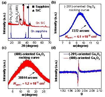
Figure 1. Presents the structural and defect analysis of epitaxial β-Ga2O3 films with different orientations: (a) XRD θ-2θ diffraction patterns for (-201)-oriented β-Ga2O3 film, (b) XRD ω scans of the (-201)-oriented β-Ga2O3 film, (c) XRD ω scans of the (400)-oriented β-Ga2O3 film, and (d) EPR characterization of (-201)-oriented and (400)-oriented β-Ga2O3 films.
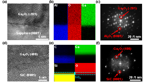
Figure 2. Presents the structural and defect analysis of epitaxial β-Ga2O3 films with different orientations: (a) HRTEM image, (b) elemental mapping, and (c) FFT pattern of the sapphire / (-201)-Ga2O3 interface, (d) HRTEM image, (e) elemental map, and (f) FFT pattern of the SiC / (400)-Ga2O3 interface.
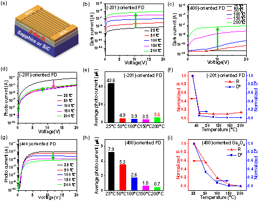
Figure 3. Performance of the MSM-PDs: (a) Schematic diagram of Ga2O3 MSM-PDs, (b) Dark current of the (-201)-oriented PD, (c) Dark current of the (400)-oriented PD, (d-f) Photo current,R and D* of the (-201)-oriented PD at different temperatures, (g-i) Photo current,R and D* of the (400)-oriented PD at different temperatures.
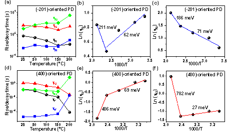
Figure 4. Temperature-dependent transient response and activation energy extraction: (a) Rise and decay times of the (-201)-oriented PD at different temperatures, (b, c) Arrhenius plots of the slow rise and decay time components for the (-201)-oriented PD, (d) Rise and decay times of the (400)-oriented PD, (e, f) Arrhenius plots of the slow rise and decay time components for the (400)-oriented PD.

Figure 5. Carrier transport mechanisms of β-Ga2O3 PDs at different temperatures: (a) (-201)-oriented PD, (b) (400)-oriented PD.
Team Introduction
The Power Semiconductor Laboratory at Xiamen University has long been engaged in innovative and exploratory research on the fundamental science, engineering technology, and industrial applications of wide-bandgap semiconductor materials and devices. Its main research areas include the epitaxial growth and doping mechanisms of GaN and Ga2O3, chip design and simulation, and chip fabrication and module integration. It has developed a series of SBD/MOSFET/HEMT power devices and SBD/MSM/PN/APD optoelectronic devices, including: (1) a series of 650 V GaN HEMT chips with on-resistance ratings of 350 mΩ/50 mΩ/25 mΩ/10 mΩ, etc., among which the 10 mΩ E-mode GaN HEMT chip exhibits the lowest on-resistance among devices of comparable specifications worldwide; and (2) a series of 650 V/1200 V/3000 V gallium oxide power devices enabled by a unique atomic nitrogen surface treatment and CuCrO2 heterojunction technology.
Introduction of the Authors

Shuaihang Xu is currently pursuing his PhD degree in Integrated Circuit Science and Engineering at Xiamen University. His research primarily focuses on the epitaxial growth of gallium oxide (Ga2O3) by molecular beam epitaxy (MBE) and metal-organic chemical vapor deposition (MOCVD), as well as the design and fabrication of optoelectronic and power devices.

Cunzhi Sun obtained his PhD degree in microelectronics and solid-state electronics from Xiamen University. He then became a visiting researcher at Technical University of Denmark and a postdoc at Xiamen University. He is currently an associate professor at Xiamen Ocean Vocational College. His research interests lie in wide bandgap semiconductors for optoelectronic applications and power electronic.

Weifeng Yang is a Minjiang Scholar Distinguished Professor and Ph.D. supervisor at Xiamen University. He was selected for the Fujian Provincial “Foreign Experts Hundred Talents Program” and the Xiamen “Double Hundred Plan” Innovative Talent Program. He previously conducted research at Nanyang Technological University, the National University of Singapore, and the Agency for Science, Technology and Research (A*STAR), Singapore. His long-term research focuses on the epitaxial growth and doping mechanisms of wide-bandgap and ultrawide-bandgap semiconductors, device design and simulation, and chip process and module integration. He has authored/co-authored more than 100 academic papers in internationally renowned academic journals and conferences, including Nature Physics, Energy Materials Storage, Advanced Science, Applied Physics Letters, IEEE Electron Device Letters, and IEEE Transactions on Electron Devices, and has applied for or been granted more than 20 invention patents.
DOI:
10.1063/5.0349846
Instruction
Official Account

Cooperation
Top
