


Researchers from the Warsaw University of Technology have published a dissertation titled " Implantation-driven metastable polymorph engineering and local silicon coordination in Ga₂O₃" in Materials & Design.
Background
The impact of impurities on the electronic properties of semiconductors is determined by their lattice localization and their interactions with structural defects. Consequently, understanding and controlling the mechanisms of impurity localization as well as defect content are essential for semiconductor device design. This holds, in particular, for gallium oxide (Ga2O3), an ultra-wide bandgap semiconductor that has garnered significant attention for its promising applications in power electronics, solar-blind optoelectronics, gas sensors, etc. Moreover, Ga2O3 exhibits strong polymorphism, which could further enhance device functionality, provided that phase transformations occurring during fabrication can be controlled.
Ion implantation is one of the primary methods for introducing dopants, and it has been used for fabricating such Ga2O3-based electronic devices such as metal–oxide–semiconductor field-effect transistor (MOSFET) channels or ohmic contacts. Historically, n-type conductivity in β-Ga2O3 was commonly attributed to oxygen vacancies. However, Varley et al. demonstrated that silicon acts as a highly effective shallow donor, establishing Si as one of the most promising dopants for achieving controllable n-type conductivity. Post-implantation annealing is conventionally used for dopant activation and crystal recovery after the implantation process, and its efficiency strongly depends on parameters such as annealing ambient, temperature, and time, demonstrating that kinetic pathways and defect evolution critically shape electrically active dopant populations. Recent studies of dopant localization in Ga2O3 have shown that Si atoms have a tendency to occupy Ga-substitutional sites under many growth and annealing conditions. Nevertheless, the substitutional vs. interstitial fraction and the local coordination are highly sensitive to the specific polymorph, implantation/processing temperature and subsequent annealing.
Abstract
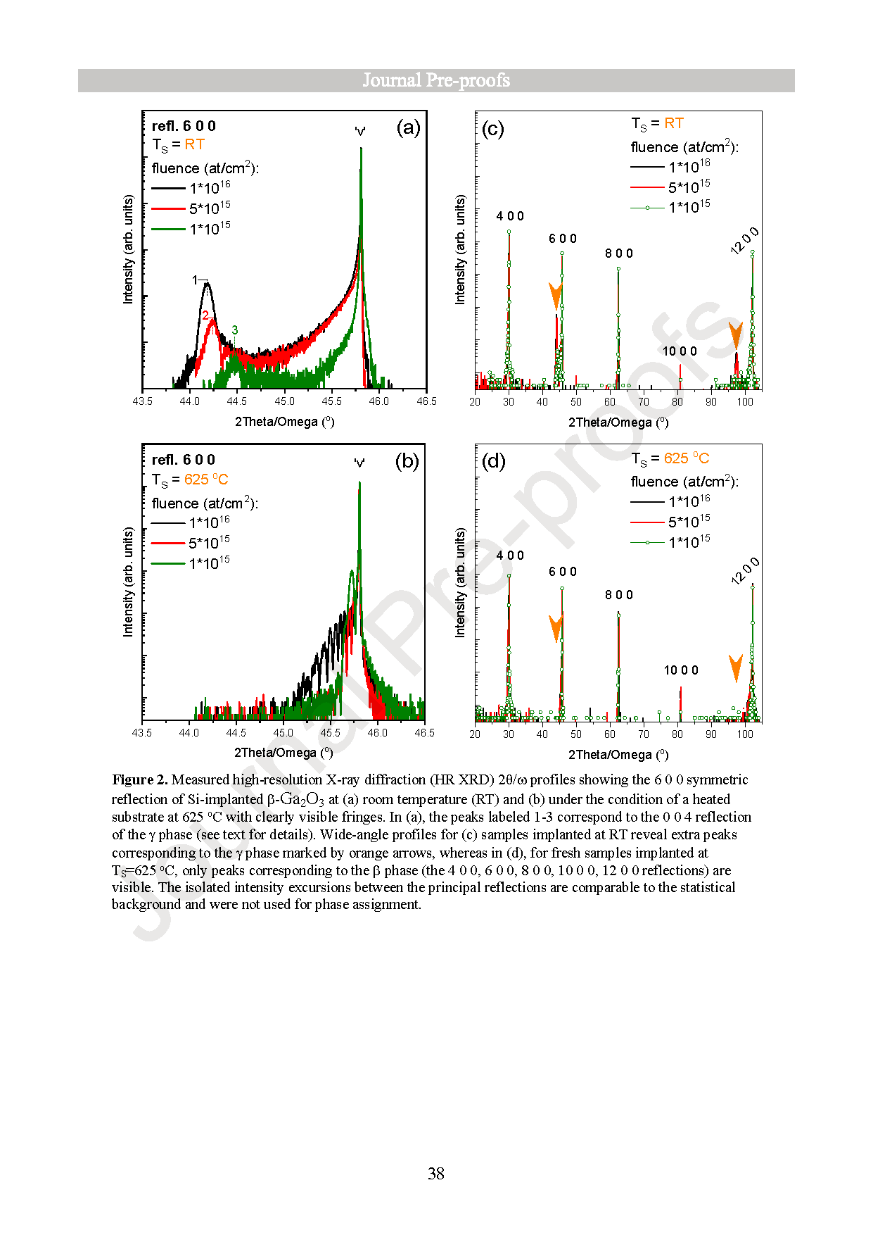
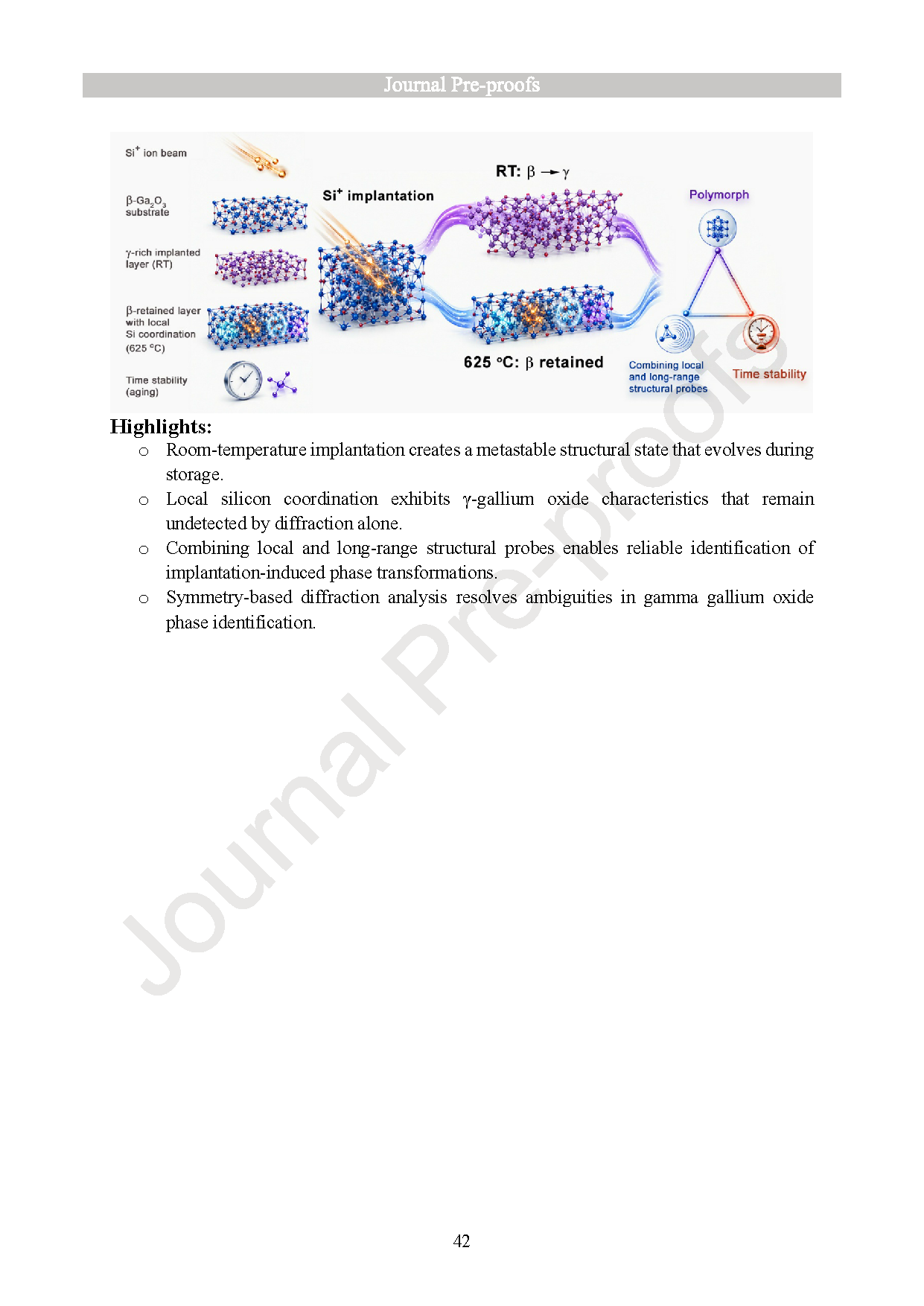
Ion implantation in gallium oxide (Ga2O3) can both introduce dopants and kinetically trap non-equilibrium polymorphs. We investigate how implantation temperature governs polymorph formation, silicon localization, and long-term structural stability in Si-implanted β-Ga2O3(100). Room-temperature implantation produces pronounced disorder and drives a disorder-mediated β → γ transformation, which is unambiguously identified by HR XRD. In contrast, implantation at 625 °C promotes dynamic defect recovery and preserves a predominantly β-Ga2O3 structure. Si K-edge XANES shows that Si is predominantly present as Si4+ but adopts polymorph-dependent local environments. In β-Ga2O3, Si is distributed between substitutional donor sites and interstitial, defect-associated configurations with γ-like coordination. In γ-Ga2O3, the Si-related contribution is preferentially associated with the intrinsically partially occupied nonspinel cation sublattice of the defective-spinel structure. A substantial Si fraction also exhibits SiO2-like coordination, consistent with partial chemical segregation and the formation of a nanoscale oxide composite within the implanted layer. After approximately one year of ambient storage, samples initially retaining predominantly β-type long-range order develop weak γ-related diffraction signatures, demonstrating delayed structural evolution of the implantation-modified state. These results show that implantation temperature, local dopant coordination, kinetic trapping, and time-dependent defect evolution must be considered together when designing implantation and subsequent thermal processing routes for Ga2O3-based materials.
Highlights
Room-temperature implantation creates a metastable structural state that evolves during storage.
Local silicon coordination exhibits γ-gallium oxide characteristics that remain undetected by diffraction alone.
Combining local and long-range structural probes enables reliable identification of implantation-induced phase transformations.
Symmetry-based diffraction analysis resolves ambiguities in gamma gallium oxide phase identification.
Conclusions
In this work, we demonstrate that ion implantation in β-Ga2O3 should be considered not only as a dopant-introduction method but also as a route for creating kinetically trapped and structurally complex material states. HR XRD, supported by RBS/channeling and Si K-edge XANES with theoretical modeling, establishes a consistent relationship between implantation temperature, long-range polymorph formation, implantation-induced disorder, and local silicon coordination. Room-temperature implantation drives a disorder-mediated β → γ transformation that can be identified non-destructively by conventional high-resolution diffraction using multiple independent crystallographic criteria. Implantation at 625 °C instead promotes dynamic defect recovery, suppresses long-range γ-phase formation, and preserves predominantly β-type crystallographic order.
Si K-edge XANES shows that the local state of implanted silicon cannot be inferred from average crystallographic symmetry alone. In β-Ga2O3, Si is distributed between substitutional donor configurations and interstitial, defect-associated configurations with locally γ-like coordination. In γ-Ga2O3, the dominant Si-related contribution is associated with the intrinsically partially occupied nonspinel Ga3/Ga4 cation environments of the defective-spinel framework. The close correspondence between these γ-phase environments and the Si-interstitial-gallium-vacancy complexes previously proposed for β-Ga2O3 provides a structural interpretation of the earlier β-phase model. In both polymorphic states, a significant fraction of Si exhibits SiO2-like coordination, consistent with partial chemical segregation and the formation of SiO2-rich nano-regions. The possible electrical consequences of these SiO2-rich nano-regions (including electrically inactive Si, carrier-scattering interfaces, and trap-related electrical inhomogeneity) are inferred from their structural and chemical character rather than demonstrated directly in the present study, and therefore require validation by dedicated electrical measurements.
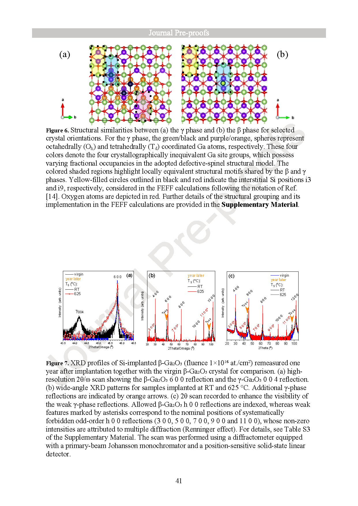
The appearance of weak γ-related diffraction signatures after approximately one year of ambient storage further demonstrates that implantation-modified Ga2O3 may continue to evolve after irradiation. Combined with the γ-like interstitial Si environments identified by XANES, this observation is consistent with a slow defect-mediated reorganization of the cation sublattice, in which locally γ-compatible configurations present in the implantation-modified β matrix progressively develop sufficient spatial correlation to become detectable by diffraction. Time should therefore be considered an additional parameter in the assessment of metastable implantation-induced structures. Although the present work concerns the as-implanted state rather than a fully processed device layer, this state defines the non-equilibrium structural starting point for subsequent annealing and can therefore influence defect recovery, dopant activation, phase stability, and the final microstructure.
Finally, these results demonstrate that implantation temperature, ion fluence, ion flux, and implantation time should be treated as coupled kinetic processing parameters. Reporting fluence alone is insufficient because the balance between defect production and dynamic recovery depends on the rate and duration of irradiation. Reliable optimization of implanted Ga2O3 therefore requires combined consideration of long-range phase identity, local dopant coordination, chemical segregation, and time-dependent defect evolution.
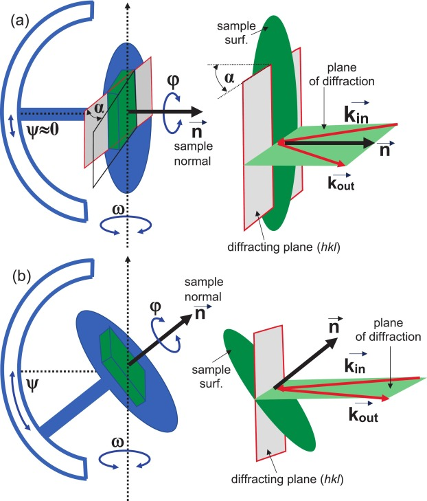
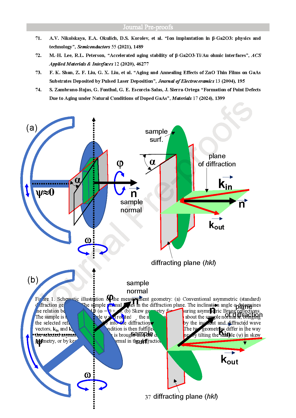
Fig. 1. Schematic illustration of the measurement geometry: (a) Conventional asymmetric (standard) diffraction geometry. The sample normal n lies in the diffraction plane. The inclination angle α determines the relation between ω and θ (ω = θ + α). (b) Skew geometry for measuring asymmetric Bragg reflections. The sample is tilted by the angle ψ and rotated by the azimuthal angle φ about the sample normal n, bringing the selected reflecting plane (hkl) into the diffraction plane defined by the incident and diffracted wave vectors, kin and kout. The Bragg condition is then fulfilled by a ω scan. The two geometries differ in the way the selected asymmetric lattice plane is brought into the diffraction plane: by tilting the sample (ψ) in skew geometry, or by keeping the sample normal in the diffraction plane in the conventional geometry.
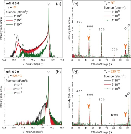
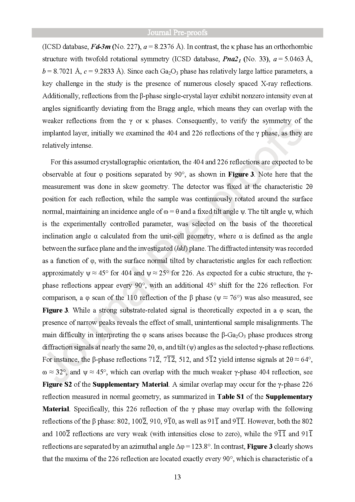
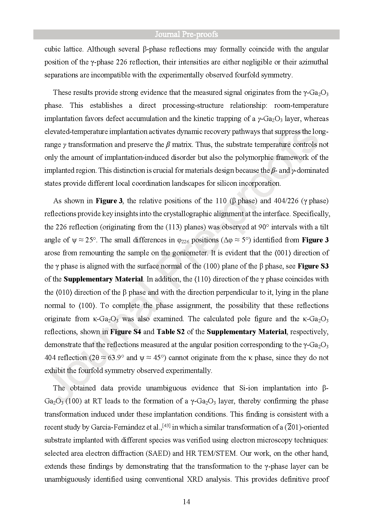
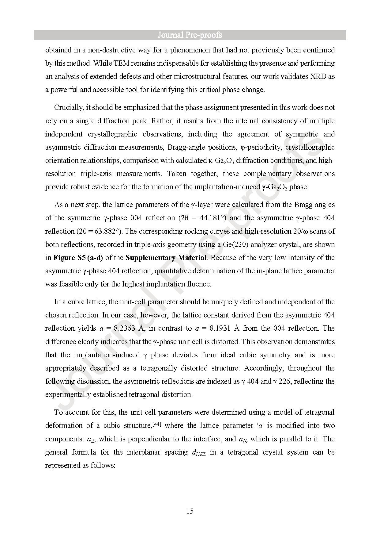
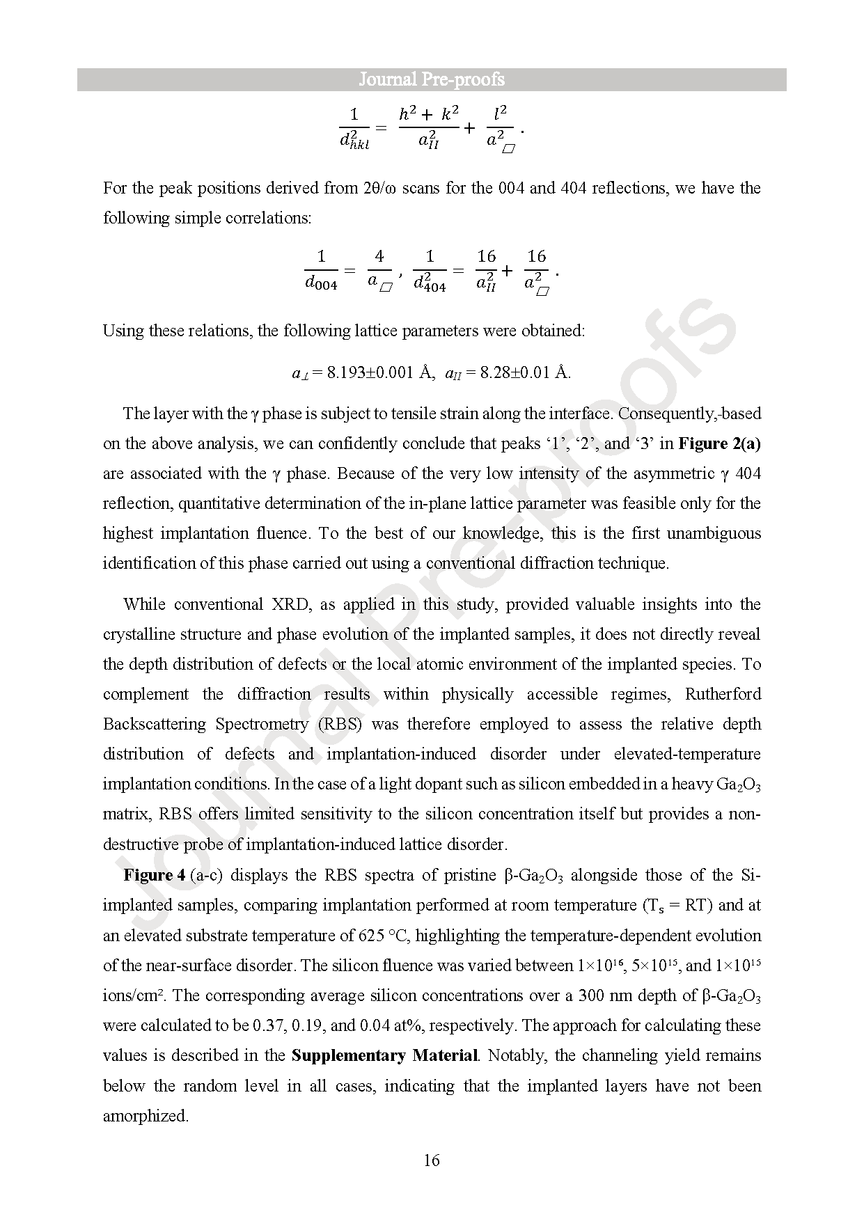
Fig. 2. Measured high-resolution X-ray diffraction (HR XRD) 2θ/ω profiles showing the 6 0 0 symmetric reflection of Si-implanted β-Ga2O3 at (a) room temperature (RT) and (b) under the condition of a heated substrate at 625 °C with clearly visible fringes. In (a), the peaks labeled 1–3 correspond to the 0 0 4 reflection of the γ phase. Wide-angle profiles for (c) samples implanted at RT reveal extra peaks corresponding to the γ phase marked by orange arrows, whereas in (d), for fresh samples implanted at TS = 625 °C, only peaks corresponding to the β phase (the 4 0 0, 6 0 0, 8 0 0, 10 0 0, 12 0 0 reflections) are visible. The isolated intensity excursions between the principal reflections are comparable to the statistical background and were not used for phase assignment.
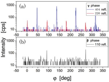
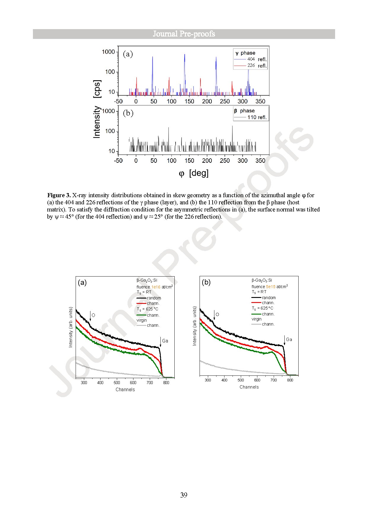
Fig. 3. X-ray intensity distributions obtained in skew geometry as a function of the azimuthal angle φ for (a) the 404 and 226 reflections of the γ phase (layer), and (b) the 110 reflection from the β phase (host matrix). To satisfy the diffraction condition for the asymmetric reflections in (a), the surface normal was tilted by ψ ≈ 45° (for the 404 reflection) and ψ ≈ 25° (for the 226 reflection).
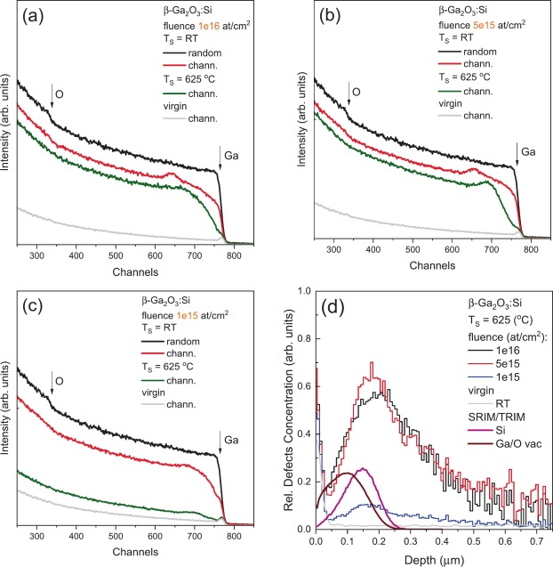
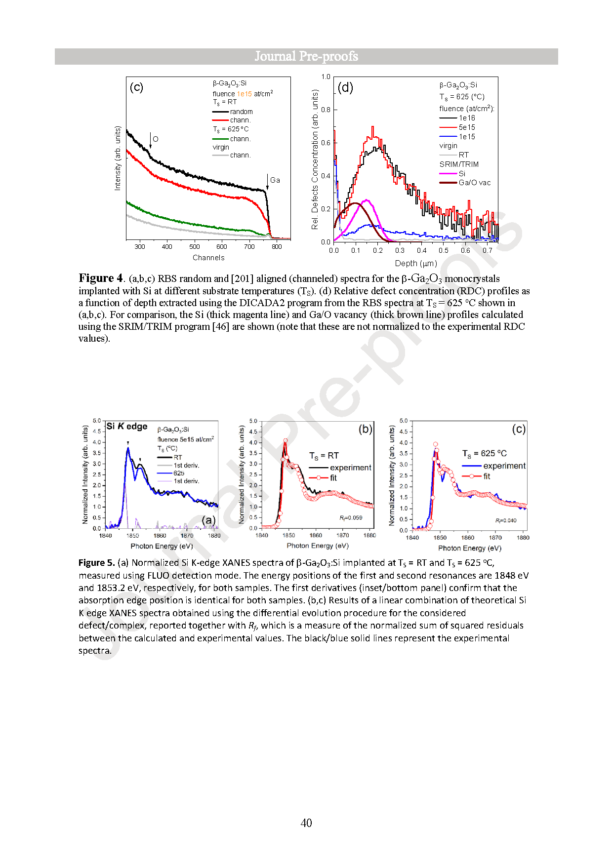
Fig. 4. (a,b,c) RBS random and [201] aligned (channeled) spectra for the β-Ga2O3 monocrystals implanted with Si at different substrate temperatures (TS). (d) Relative defect concentration (RDC) profiles as a function of depth extracted using the DICADA2 program from the RBS spectra at TS = 625 °C shown in (a,b,c). For comparison, the Si (thick magenta line) and Ga/O vacancy (thick brown line) profiles calculated using the SRIM/TRIM program are shown (note that these are not normalized to the experimental RDC values).
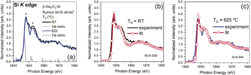
Fig. 5. (a) Normalized Si K-edge XANES spectra of β-Ga2O3:Si implanted at TS = RT and TS = 625 °C, measured using FLUO detection mode. The energy positions of the first and second resonances are 1848 eV and 1853.2 eV, respectively, for both samples. The first derivatives (inset/bottom panel) confirm that the absorption edge position is identical for both samples. (b,c) Results of a linear combination of theoretical Si K edge XANES spectra obtained using the differential evolution procedure for the considered defect/complex, reported together with Rf, which is a measure of the normalized sum of squared residuals between the calculated and experimental values. The black/blue solid lines represent the experimental spectra. (For interpretation of the references to colour in this figure legend, the reader is referred to the web version of this article.)
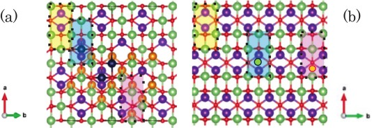
Fig. 6. Structural similarities between (a) the γ phase and (b) the β phase for selected crystal orientations. For the γ phase, the green/black and purple/orange, spheres represent octahedrally (Oh) and tetrahedrally (Td) coordinated Ga atoms, respectively. These four colors denote the four crystallographically inequivalent Ga site groups, which possess varying fractional occupancies in the adopted defective-spinel structural model. The colored shaded regions highlight locally equivalent structural motifs shared by the β and γ phases. Yellow-filled circles outlined in black and red indicate the interstitial Si positions i3 and i9. Oxygen atoms are depicted in red. Further details of the structural grouping and its implementation in the FEFF calculations are provided in the Supplementary Material.
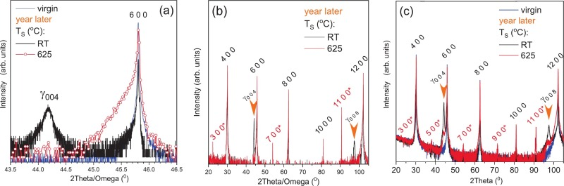
Fig. 7. XRD profiles of Si-implanted β-Ga2O3 (fluence 1 × 101⁶ at./cm2) remeasured one year after implantation together with the virgin β-Ga2O3 crystal for comparison. (a) high-resolution 2θ/ω scan showing the β-Ga2O3 6 0 0 reflection and the γ-Ga2O3 0 0 4 reflection. (b) wide-angle XRD patterns for samples implanted at RT and 625 °C. Additional γ-phase reflections are indicated by orange arrows. (c) 2θ scan recorded to enhance the visibility of the weak γ-phase reflections. Allowed β-Ga2O3 h 0 0 reflections are indexed, whereas weak features marked by asterisks correspond to the nominal positions of systematically forbidden odd-order h 0 0 reflections (3 0 0, 5 0 0, 7 0 0, 9 0 0 and 11 0 0), whose non-zero intensities are attributed to multiple diffraction (Renninger effect). For details, see Table S3 of the Supplementary Material. The scan was performed using a diffractometer equipped with a primary-beam Johansson monochromator and a position-sensitive solid-state linear detector. (For interpretation of the references to colour in this figure legend, the reader is referred to the web version of this article.)
DOI:
doi.org/10.1016/j.matdes.2026.117347

Instruction
Official Account

Cooperation
Top
