


Researchers from Nanjing University of Posts and Telecommunications have published a dissertation titled β-Ga₂O₃-Based Solar-Blind Ultraviolet Event-Based Sensor in IEEE Transactions on Electron Devices.
Background
Solar‑blind ultraviolet detection within 200‑280 nm is suitable for safety‑critical applications such as grid flame alarm and corona discharge monitoring. Nevertheless, most commercial and research‑grade UV detectors adopt conventional frame‑integrated imaging architectures, which fail to satisfy the requirements of real‑time dynamic capture and low‑power edge computing for safety monitoring.
Aluminum gallium nitride (AlGaN) is the dominant material for existing UV event sensors. High‑aluminum composition is required to achieve solar‑blind UV response, which degrades crystal quality and increases manufacturing costs.
As an emerging ultrawide‑bandgap semiconductor, β‑Ga₂O₃ possesses an intrinsic bandgap of ~4.9 eV, excellent thermal and chemical stability, making it an ideal candidate for solar‑blind UV photodetection. However, monolithically integrated devices targeted for event‑driven sensing remain to be developed.
Most existing event cameras work in visible and infrared bands. The development of solar-blind UV event sensors is limited by materials, as the devices exhibit poor dynamic response.
Abstract
In this work, β-Ga₂O₃ thin films were grown on sapphire substrates via metal‑organic chemical vapor deposition (MOCVD). The triethylgallium precursor flow rate was modulated to maintain oxygen‑vacancy concentration at a proper low level, suppressing oxygen‑vacancy‑induced carrier trapping‑relaxation effect and obtaining photosensitive thin films with fast photoresponse. A 254 nm solar‑blind UV event sensor was fabricated by monolithically integrating β‑Ga₂O₃ photodetectors with dual‑channel complementary event‑processing circuits.
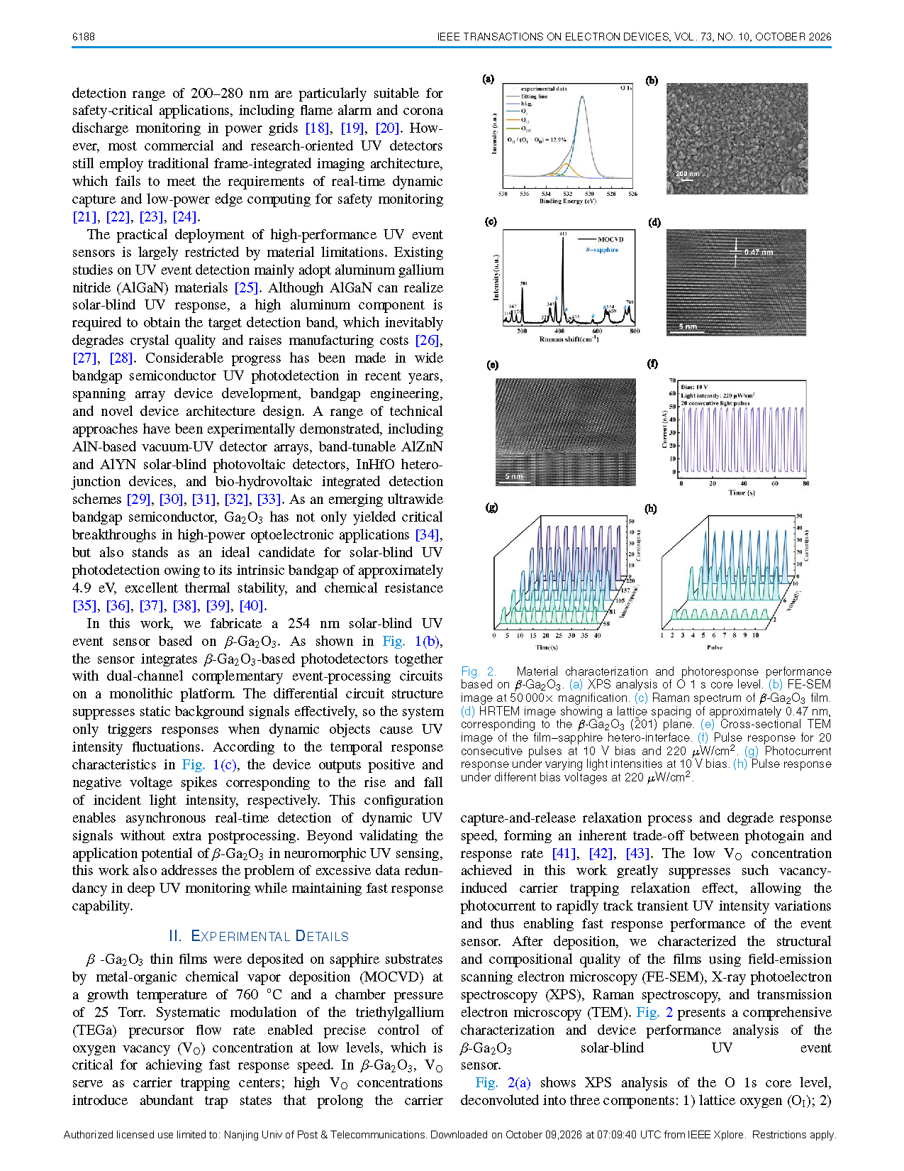
Material characterizations: X‑ray photoelectron spectroscopy (XPS), field‑emission scanning electron microscopy (FE‑SEM), Raman spectroscopy, high‑resolution transmission electron microscopy (HRTEM) and cross‑sectional TEM were adopted to evaluate film quality. XPS gives OII/(OI+OII)≈12.9%, confirming moderate oxygen vacancies within films. The films are dense and uniform without cracks or voids. Raman measurements verify high‑purity monoclinic β-Ga₂O₃ phase. HRTEM yields a lattice spacing of 0.47 nm corresponding to the β-Ga₂O₃ () plane. The hetero‑interface between β-Ga₂O₃ film and sapphire substrate exhibits favorable bonding quality.
Photopulse measurements: Twenty consecutive light‑pulse cycles were tested under 10 V bias and 220 μW/cm². The photocurrent amplitude remains stable with no baseline drift of dark current, maintaining a high photocurrent‑to‑dark‑current ratio. Stable pulse outputs are obtained under varied light intensities and bias voltages ranging from 2 V to 10 V. Output signals are susceptible to noise at low bias; hence 10 V is selected as the operating voltage. Future work will focus on self‑powered solar‑blind UV event cameras.
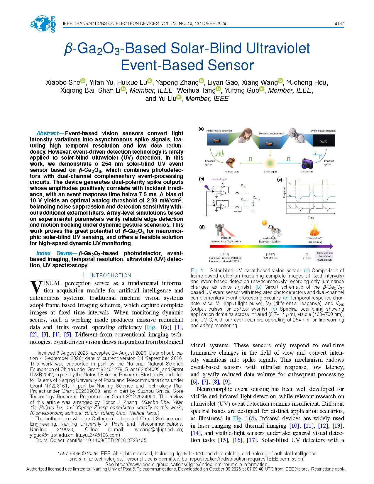
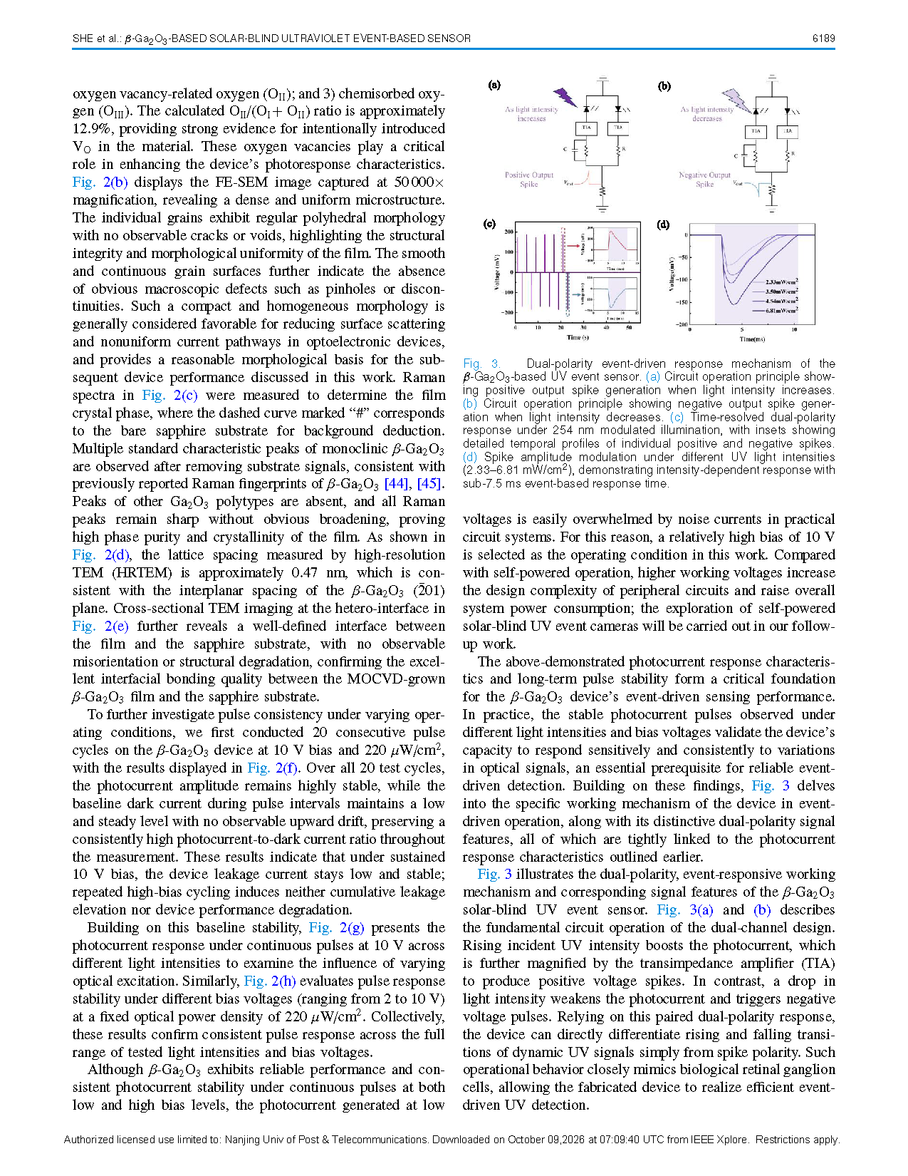
Event‑driven working mechanism: The dual‑channel differential circuit effectively suppresses static background signals. Output is triggered only when dynamic UV‑intensity fluctuation occurs. Positive voltage spikes are generated upon light‑intensity rise, and negative spikes upon light‑intensity fall. Spike polarity directly indicates intensity increase or decrease, mimicking biological retinal ganglion cells. Asynchronous real‑time detection of dynamic UV signals is realized with an event response time below 7.5 ms.
Research significance: This work validates the application potential of β-Ga₂O₃ for neuromorphic UV sensing and mitigates data redundancy in deep‑UV monitoring while preserving fast‑response capability.
Hightlights
Device‑architecture innovation: Monolithic integration of β-Ga₂O₃ photosensitive units and dual‑channel complementary event‑processing circuits is realized. The differential circuit suppresses static background noise and generates outputs only for dynamic light‑intensity variations.
Material‑modulation innovation: Precursor flow is tuned in the MOCVD process to precisely control oxygen‑vacancy concentration, restrain vacancy‑related carrier trapping‑relaxation, and alleviate the inherent trade‑off between photogain and response speed.
Signal‑mechanism innovation: Dual‑polarity event spike output is achieved. Positive pulses correspond to rising light intensity and negative pulses to falling light intensity. Variations of UV signals can be directly distinguished by spike polarity without complicated post‑processing, imitating retinal ganglion cells.
Application‑oriented innovation: Introduce the event-driven retinal dynamic vision mechanism into solar-blind ultraviolet detection to overcome the data redundancy drawback of traditional frame imaging, realize high-speed asynchronous ultraviolet detection, and support practical applications of deep ultraviolet.
Conclusions
A monolithically integrated solar‑blind UV event sensor based on MOCVD‑grown β‑Ga₂O₃ thin film is successfully fabricated. The thin film possesses outstanding crystallinity and hetero‑interface quality, and fast photoresponse is realized via oxygen‑vacancy engineering.
The device exhibits stable pulse outputs under various light intensities and bias voltages. It generates positive‑and‑negative dual‑polarity voltage spikes with event response time below 7.5 ms, enabling asynchronous capture of dynamic UV‑intensity changes and static‑background suppression.
This device demonstrates that β-Ga₂O₃ is applicable to neuromorphic solar‑blind UV event sensing and can alleviate data redundancy in deep‑UV monitoring.
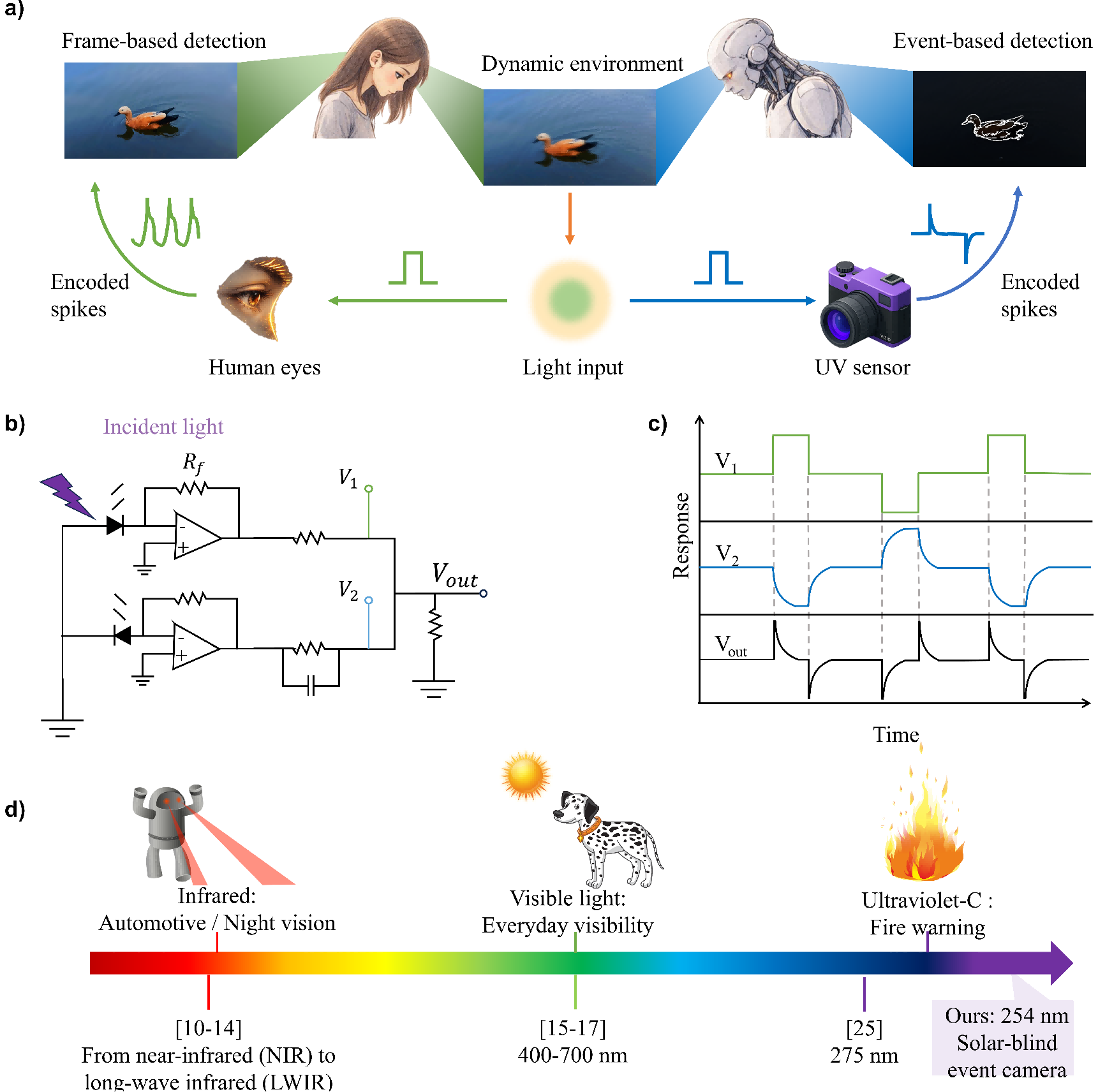
Fig. 1 Solar-blind UV event-based vision sensor. (a) Comparison of frame-based detection (capturing complete images at fixed intervals) and event-based detection (asynchronously recording only luminance changes as spike signals). (b) Circuit schematic of the β-Ga₂O₃-based UV event sensor with integrated photodetectors and dual-channel complementary event-processing circuitry. (c) Temporal response characteristics: V1 (input light pulse), V2 (differential response), and Vout (output pulses for ON/OFF events). (d) Spectral positioning showing application domains across infrared (0.7-14 μm), visible (400-700 nm), and UV-C, with our event camera operating at 254 nm for fire warning and safety monitoring.
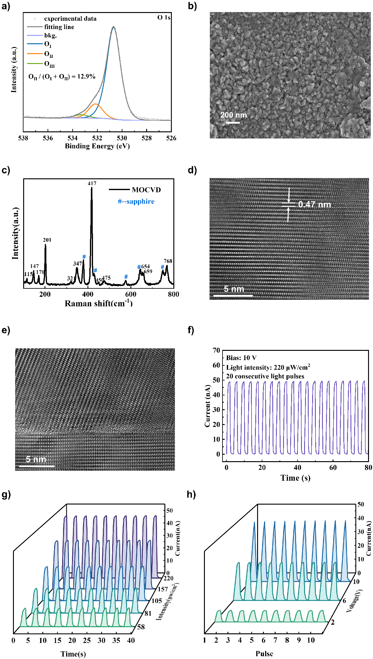
Fig. 2 Material characterization and photoresponse performance based on β-Ga₂O₃. (a) XPS analysis of O 1s core level. (b) FE-SEM image at 50,000× magnification. (c) Raman spectrum of β-Ga₂O₃ film. (d) HRTEM image showing a lattice spacing of approximately 0.47 nm, corresponding to the β-Ga₂O₃ () plane. (e) Cross-sectional TEM image of the film–sapphire hetero‑interface. (f) Pulse response for 20 consecutive pulses at 10 V bias and 220 μW/cm2. (g) Photocurrent response under varying light intensities at 10 V bias. (h) Pulse response under different bias voltages at 220 μW/cm2.
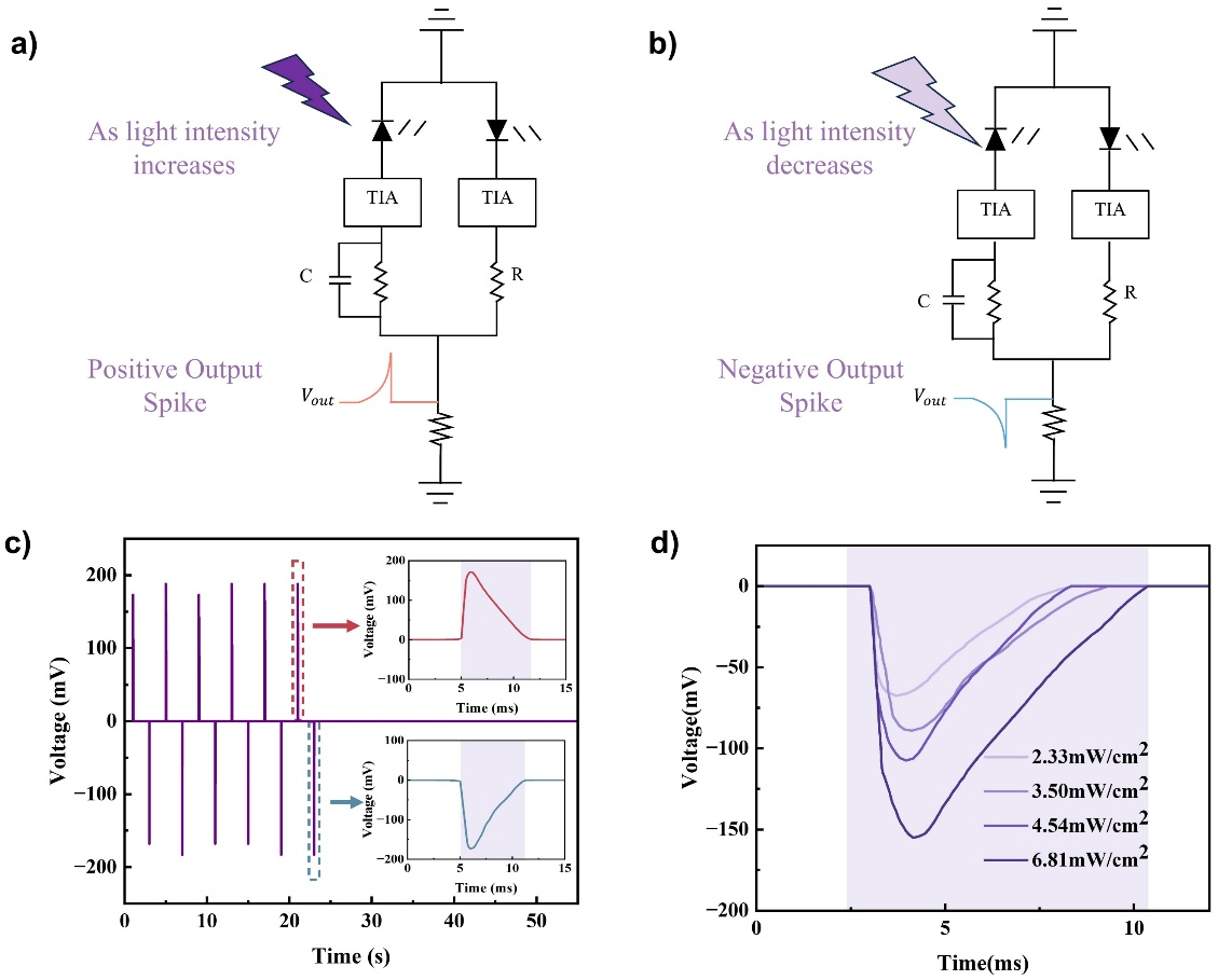
Fig. 3 Dual-polarity event-driven response mechanism of the β-Ga₂O₃-based UV event sensor. (a) Circuit operation principle showing positive output spike generation when light intensity increases. (b) Circuit operation principle showing negative output spike generation when light intensity decreases. (c) Time-resolved dual-polarity response under 254 nm modulated illumination, with insets showing detailed temporal profiles of individual positive and negative spikes. (d) Spike amplitude modulation under different UV light intensities (2.33-6.81 mW/cm2), demonstrating intensity-dependent response with sub-7.5 ms event-based response time.
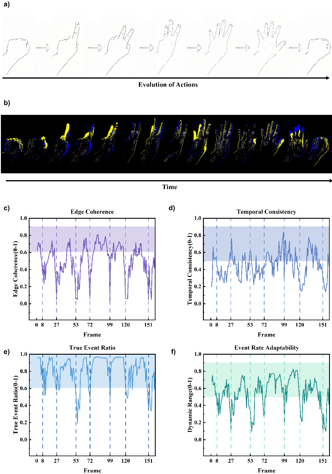
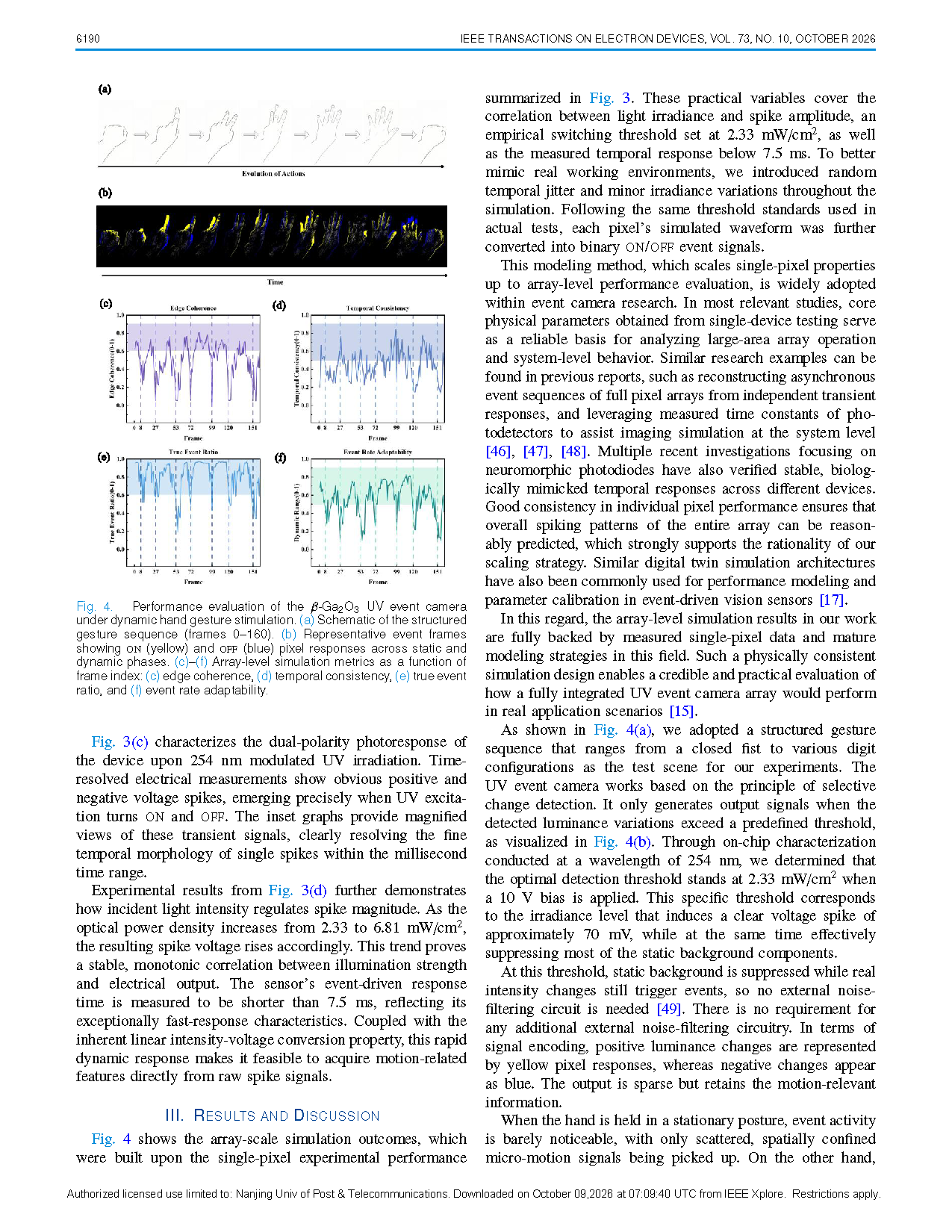
Fig. 4 Performance evaluation of the β-Ga₂O₃ UV event camera under dynamic hand gesture stimulation. (a) Schematic of the structured gesture sequence (frames 0-160). (b) Representative event frames showing ON (yellow) and OFF (blue) pixel responses across static and dynamic phases. (c-f) Array-level simulation metrics as a function of frame index: edge coherence (c), temporal consistency (d), true event ratio (e), and event rate adaptability (f).
DOI:
doi.org/10.1109/TED.2026.3728405
Instruction
Official Account

Cooperation
Top
