


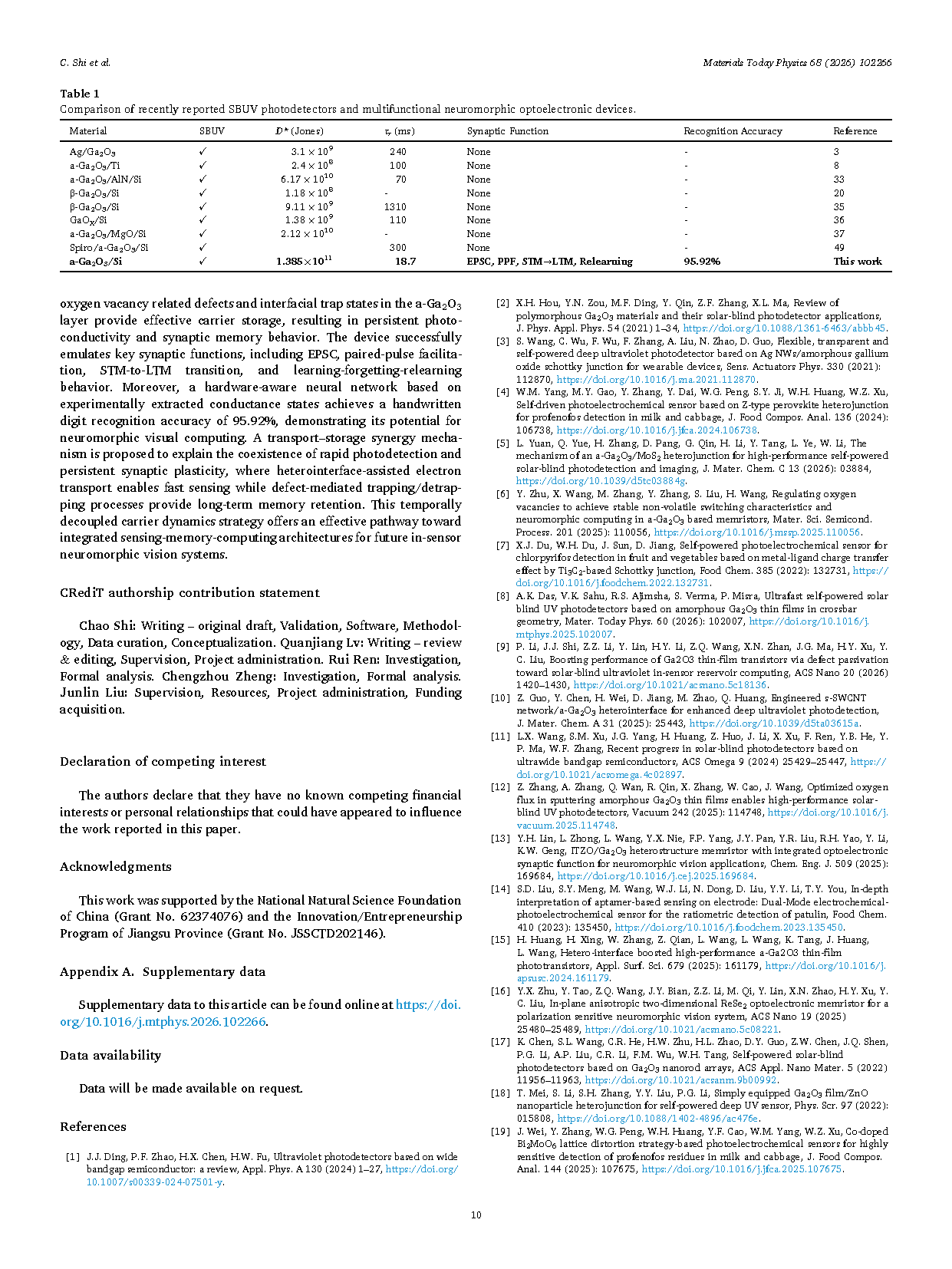
The research team led by Junlin Liu and Quanjiang Lv at Jiangsu University published an article in the academic journal Materials Today Physics entitled Synergistic Fast Carrier Extraction and Persistent Synaptic Plasticity in an Amorphous Ga2O3/Si Heterojunction for Solar-Blind Photodetection and Neuromorphic Computing.
Background
With the rapid development of artificial intelligence and edge computing, optoelectronic synaptic devices that integrate optical sensing, information storage, and computing have become an important research direction in neuromorphic vision. Gallium oxide (Ga2O3), a representative ultra-wide-bandgap semiconductor, offers excellent solar-blind ultraviolet (SBUV) selectivity, chemical stability, and a high breakdown electric field, making it promising for SBUV detection and brain-inspired vision systems. Amorphous Ga2O3 (a-Ga2O3) offers advantages including low-temperature fabrication, uniform large-area deposition, and good substrate compatibility. Its defect-related states may also produce persistent photoconductivity through carrier trapping and release, providing a material basis for integrating photodetection and synaptic memory. However, the intrinsically low carrier mobility of a-Ga2O3 limits efficient carrier transport. Meanwhile, although defect-induced persistent photoconductivity benefits information storage, it may prolong device response times, making it difficult to achieve both fast photoresponse and long-term memory. To address this challenge, an a-Ga2O3/Si heterojunction can be constructed to introduce a high-mobility Si transport channel and use interfacial carrier regulation to improve carrier extraction while retaining the photoelectric memory associated with defect-related states. This strategy offers a new approach to integrating SBUV detection with neuromorphic visual computing.
Abstract
This work designed and fabricated a SBUV photodetector based on an a-Ga2O3/Si heterojunction and further explored its application in neuromorphic vision computing. The a-Ga2O3 film was deposited on a p-type Si substrate by magnetron sputtering. Comparison with a device fabricated on a sapphire substrate demonstrated the beneficial role of the Si transport channel in carrier transport and photodetection performance. The heterojunction device achieved a responsivity of 182 mA/W and a specific detectivity of 1.39 × 10¹¹ Jones, with a rise time of 18.7 ms, while exhibiting excellent SBUV selectivity and environmental stability. Furthermore, under 254 nm UV pulse stimulation, the device exhibited typical synaptic behaviors, including excitatory postsynaptic current (EPSC), paired-pulse facilitation (PPF), the transition from short-term to long-term memory, and learning–forgetting–relearning. These characteristics demonstrate its dynamic response and memory capabilities under optical stimulation. In addition, the experimentally measured conductance characteristics of the device were incorporated into a convolutional neural network (CNN) simulation, achieving an MNIST handwritten-digit recognition accuracy of 95.92%, close to the 96.73% accuracy of the ideal software model. These results demonstrate the integration of SBUV photodetection and optoelectronic synaptic functionality in an a-Ga2O3/Si heterojunction, offering a new approach to developing devices that combine optical sensing and information processing for neuromorphic vision systems.
Highlights
① Proposed a Heterojunction Design Strategy for Synergistic Carrier Transport and Storage: By integrating a-Ga2O3 with high-mobility Si, the heterojunction promotes carrier transport while exploiting defect states in a-Ga2O3 for carrier storage, offering a new device design strategy for integrating fast photodetection with optoelectronic memory.
② Analysis of Carrier Trapping–Detrapping Dynamics and the Persistent Photoconductivity Mechanism: The synergistic relationship between carrier transport in the heterojunction and defect-related trapping–detrapping processes in a-Ga2O3 is elucidated, clarifying the persistent photoconductivity effect and its influence on optoelectronic synaptic memory behavior. This provides a physical basis for understanding the synaptic plasticity of the device.
③ Integrated SBUV Photodetection and Optoelectronic Synaptic Functionality: SBUV photodetection and biomimetic synaptic behaviors are integrated into a single a-Ga2O3/Si heterojunction device, enabling the functional integration of optical signal sensing, dynamic carrier response, and synapse-like information processing, thereby expanding its potential applications in neuromorphic vision.
Project Support
This work was supported by the National Natural Science Foundation of China (Grant No. 62374076) and the Jiangsu Innovation and Entrepreneurship Program (Grant No. JSSCTD202146).
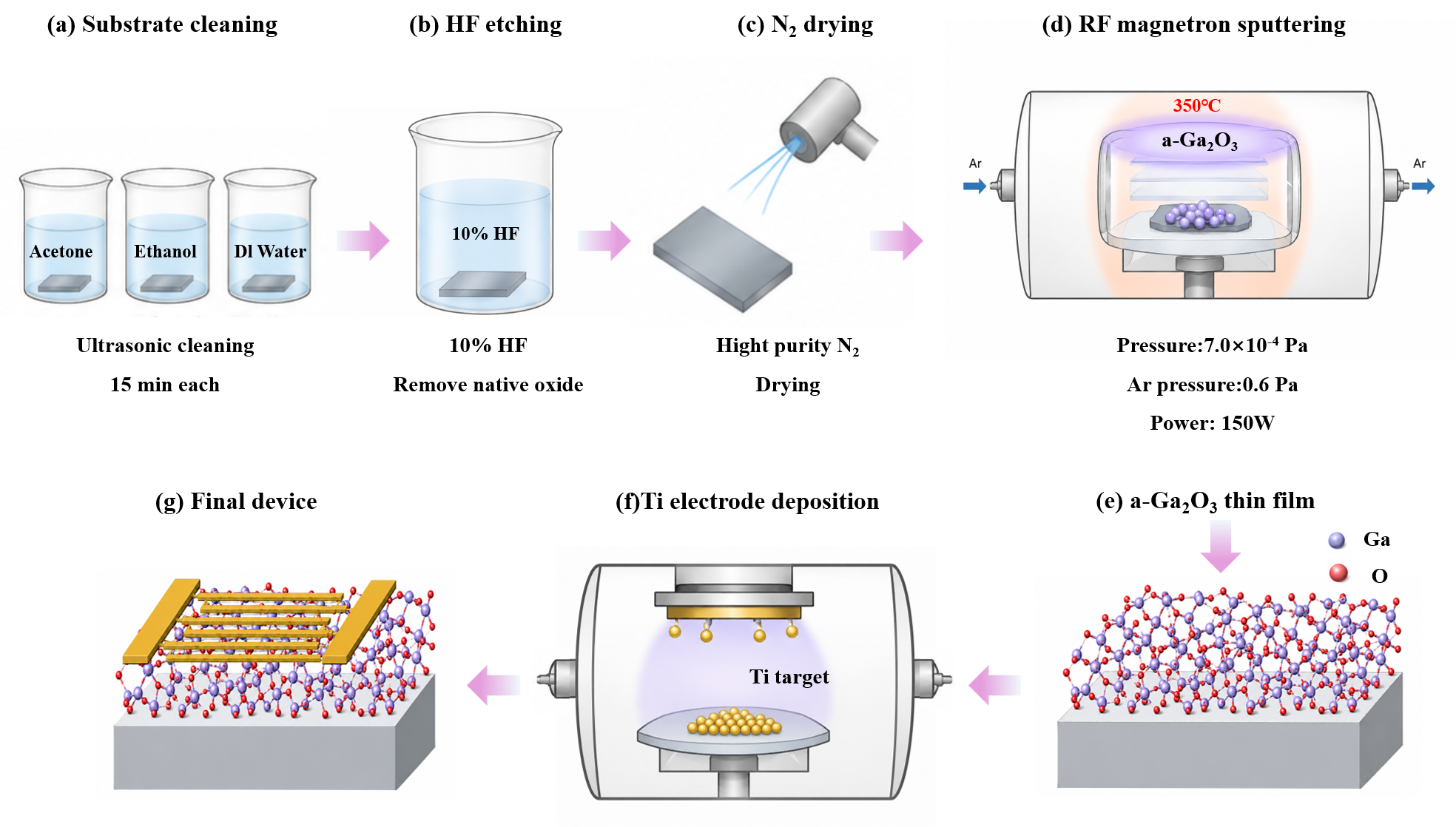
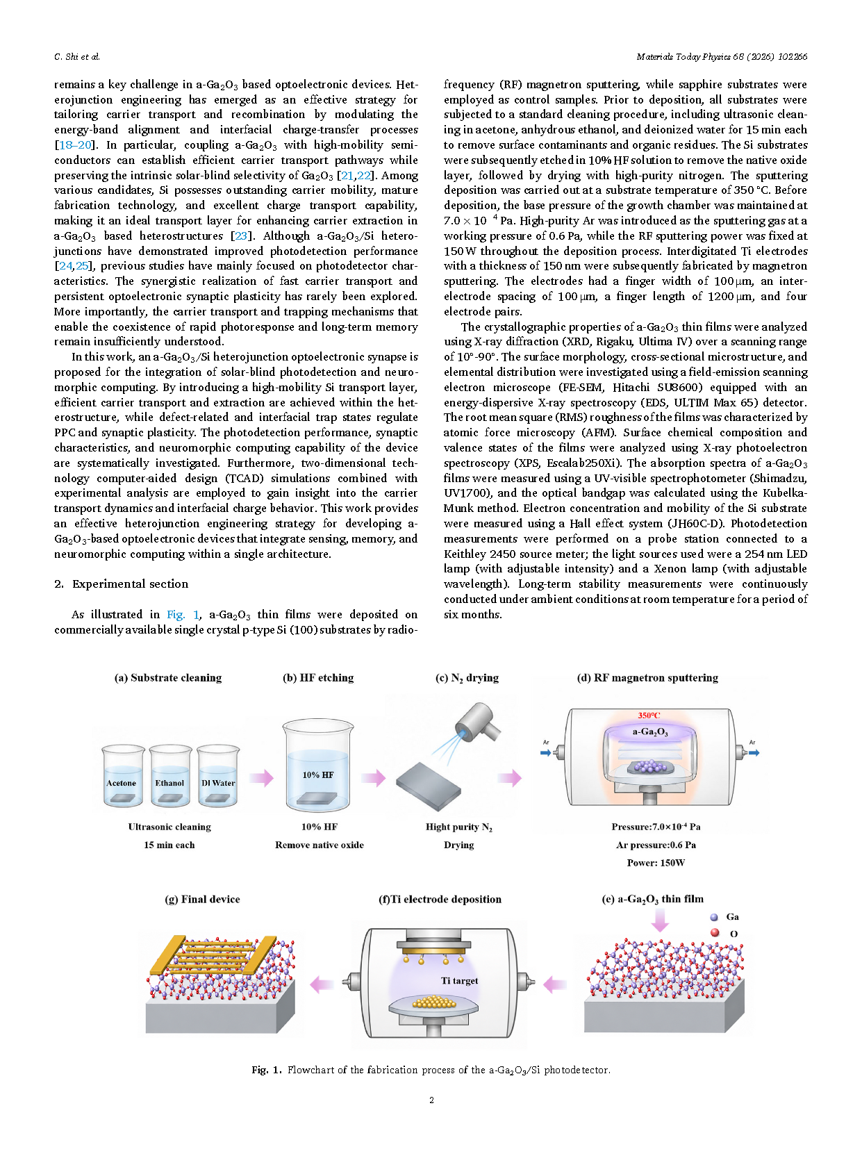
Figure 1. Flowchart of the fabrication process of the a-Ga2O3/Si photodetector.
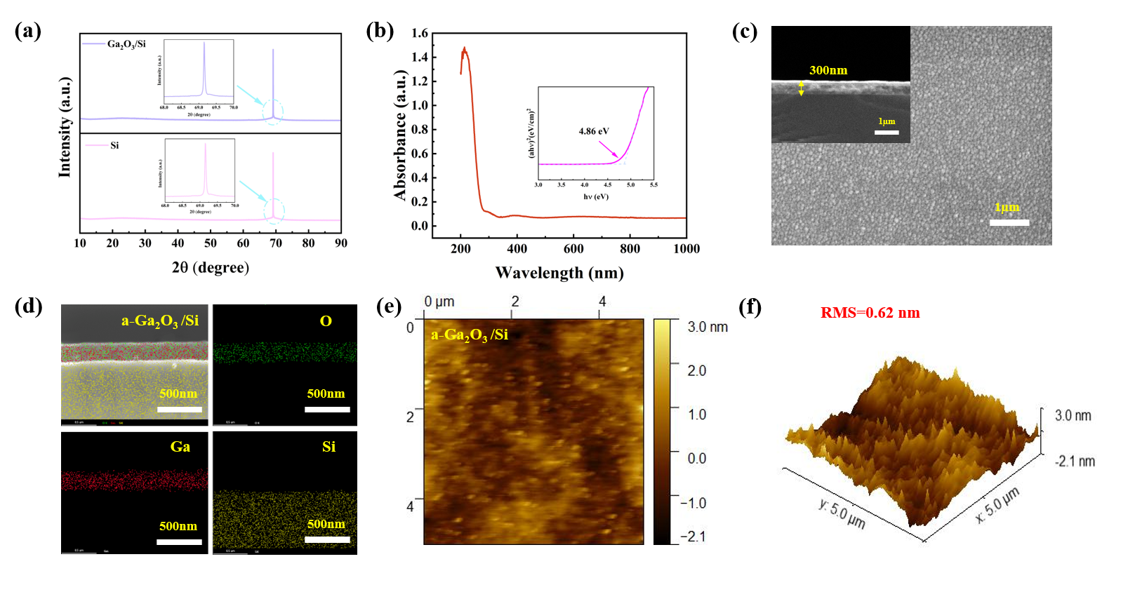
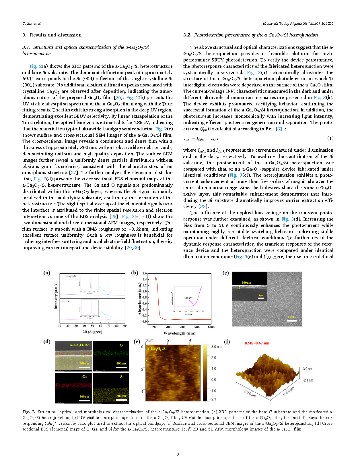
Figure 2. Structural, optical, and morphological characterization of the a-Ga2O3/Si heterojunction.(a) XRD patterns of the bare Si substrate and the fabricated a-Ga2O3/Si heterojunction; (b) UV-visible absorption spectrum of the a-Ga2O3 film, UV-visible absorption spectrum of the a-Ga2O3 film, the inset displays the corresponding versus Tauc plot used to extract the optical bandgap; (c) Surface and cross-sectional SEM images of the a-Ga2O3/Si heterojunction; (d) Cross-sectional EDS elemental maps of O, Ga, and Si for the a-Ga2O3/Si heterostructure; (e, f) 2D and 3D AFM morphology images of the a-Ga2O3 film.
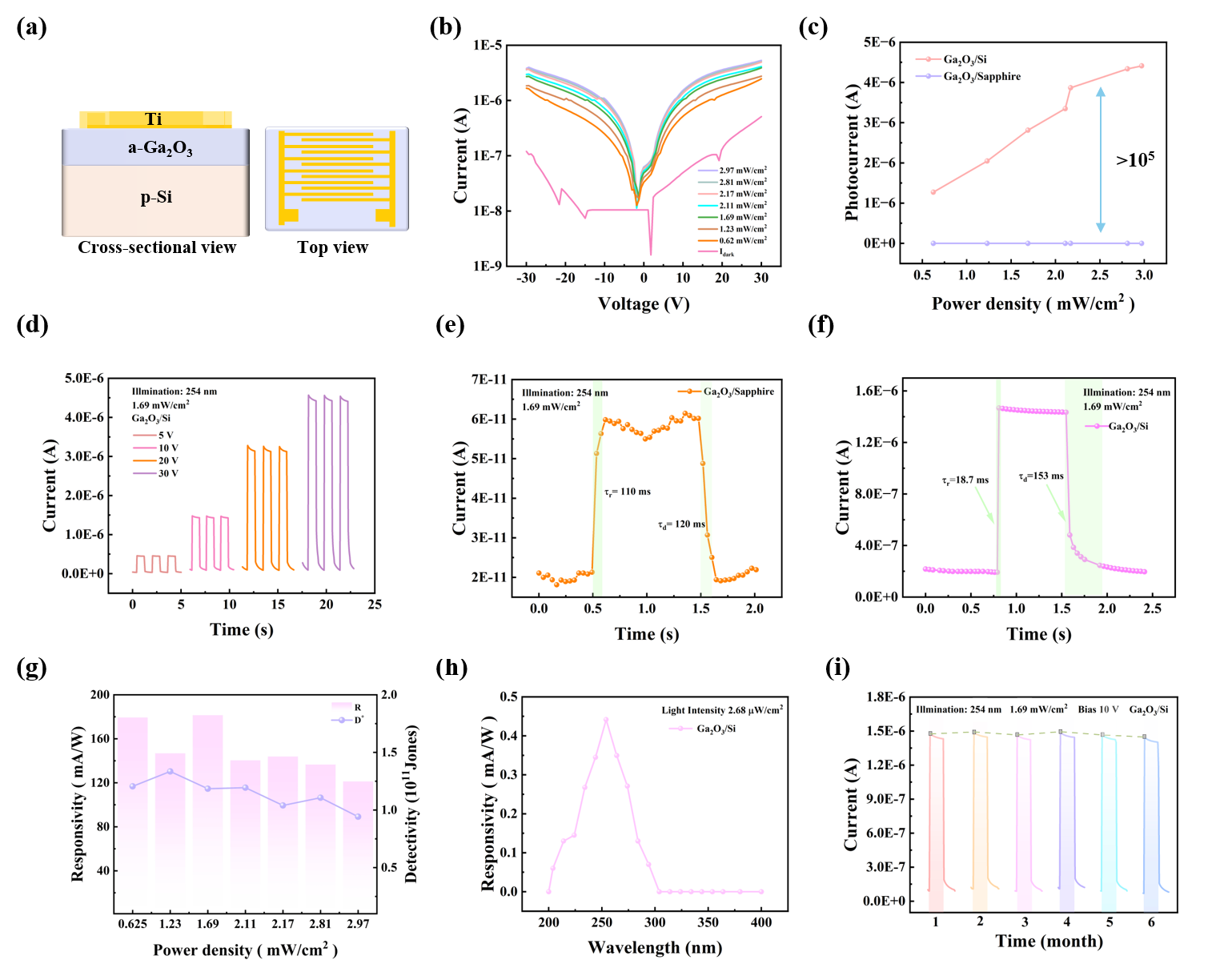
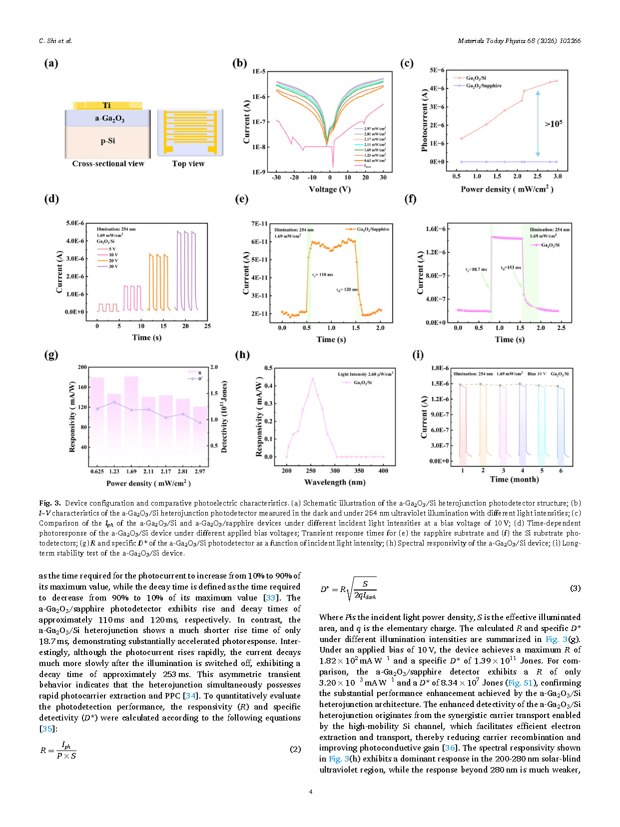
Figure 3. Device configuration and comparative photoelectric characteristics. (a) Schematic illustration of the a-Ga2O3/Si heterojunction photodetector structure; (b) I–V characteristics of the a-Ga2O3/Si heterojunction photodetector measured in the dark and under 254 nm ultraviolet illumination with different light intensities; (c) Comparison of the Iph of the a-Ga2O3/Si and a-Ga2O3/sapphire devices under different incident light intensities at a bias voltage of 10 V; (d) Time-dependent photoresponse of the a-Ga2O3/Si device under different applied bias voltages; Transient response times for (e) the sapphire substrate and (f) the Si substrate photodetectors; (g) R and specific D* of the a-Ga2O3/Si photodetector as a function of incident light intensity; (h) Spectral responsivity of the a-Ga2O3/Si device ; (i) Long-term stability test of the a-Ga2O3/Si device.
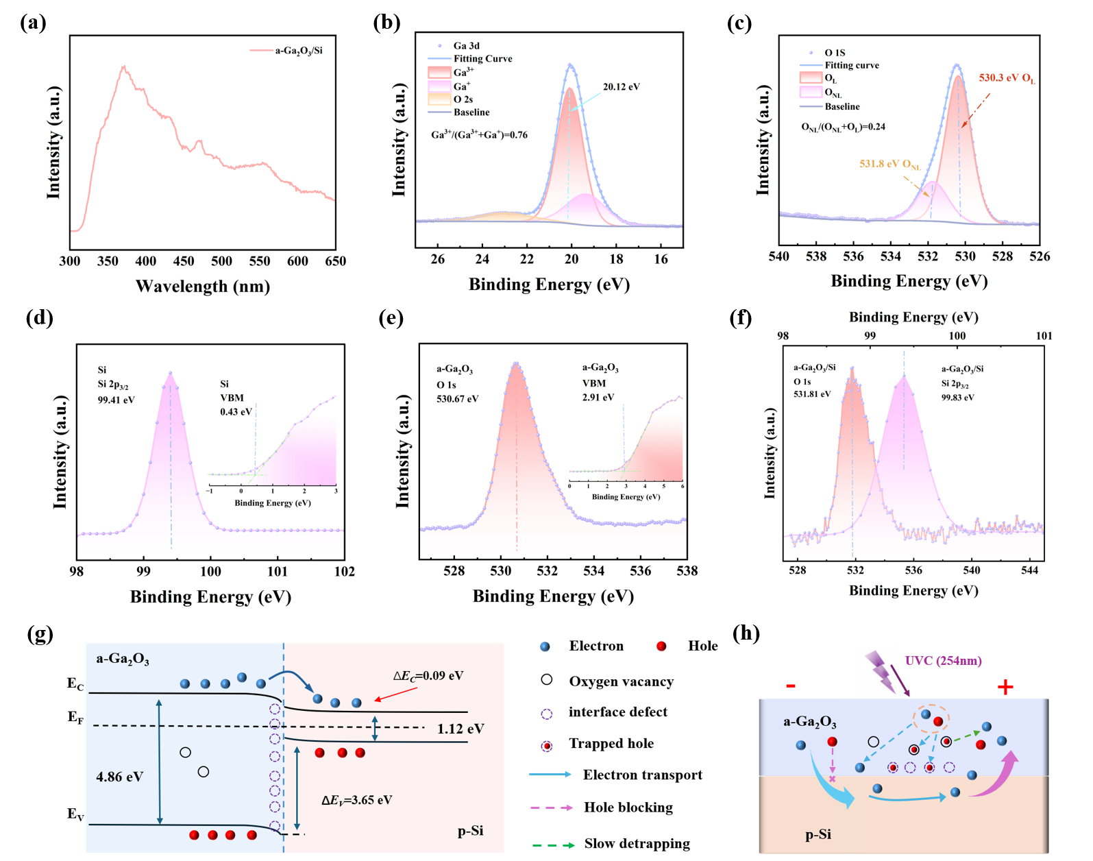
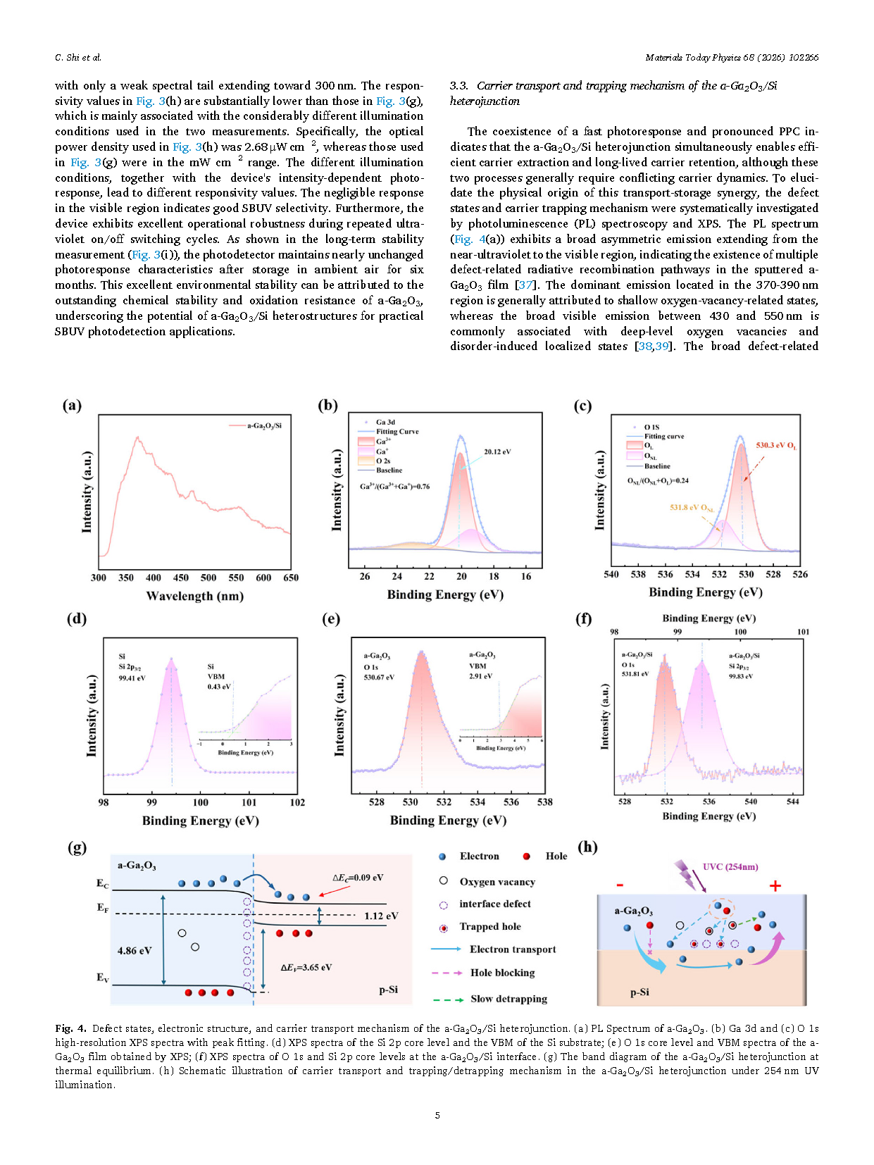
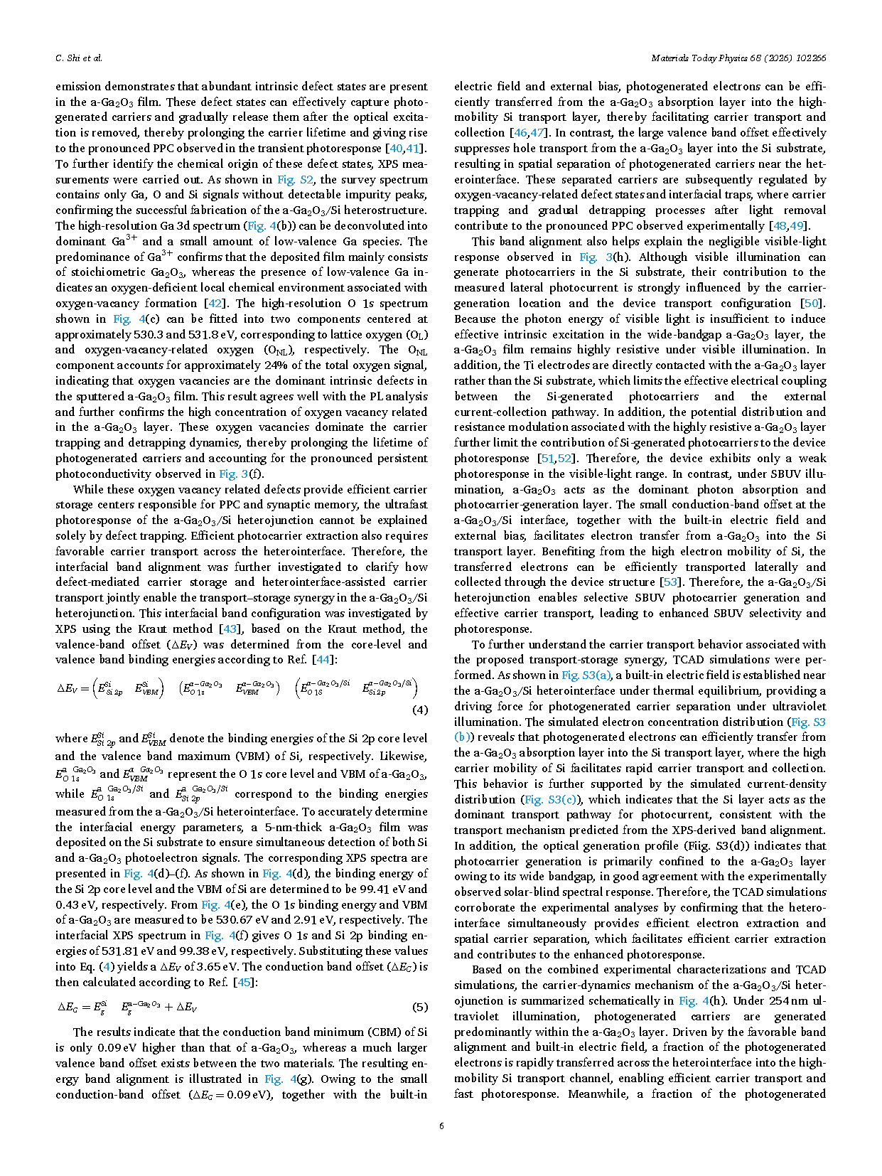
Figure 4. Defect states, electronic structure, and carrier transport mechanism of the a-Ga2O3/Si heterojunction. (a) PL Spectrum of a-Ga2O3. (b) Ga 3d and (c) O 1s high-resolution XPS spectra with peak fitting. (d) XPS spectra of the Si 2p core level and the VBM of the Si substrate; (e) O 1s core level and VBM spectra of the a-Ga2O3 film obtained by XPS; (f) XPS spectra of O 1s and Si 2p core levels at the a-Ga2O3/ Si interface. (g) The band diagram of the a-Ga2O3/Si heterojunction at thermal equilibrium. (h) Schematic illustration of carrier transport and trapping/detrapping mechanism in the a-Ga2O3/Si heterojunction under 254 nm UV illumination.
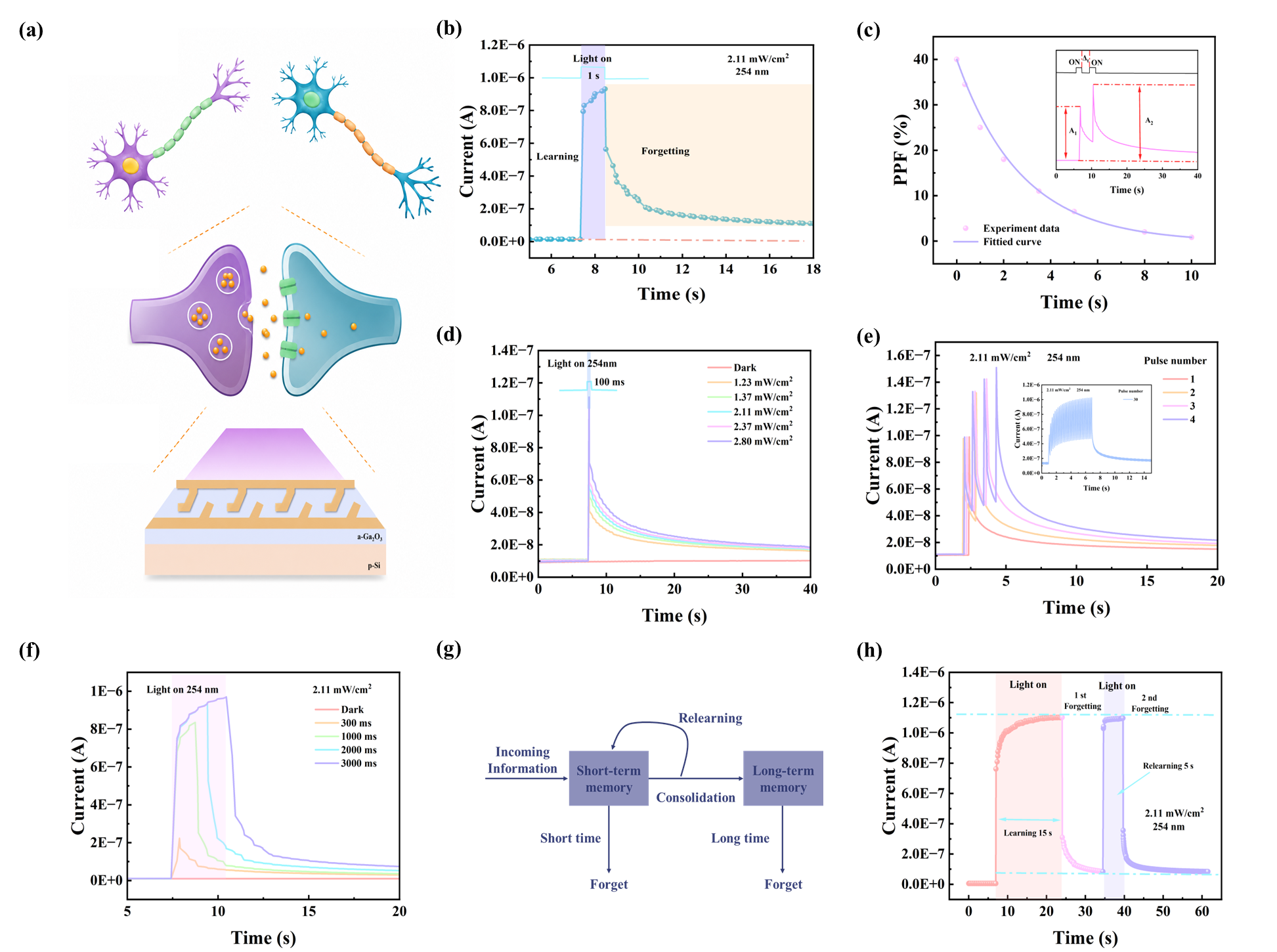
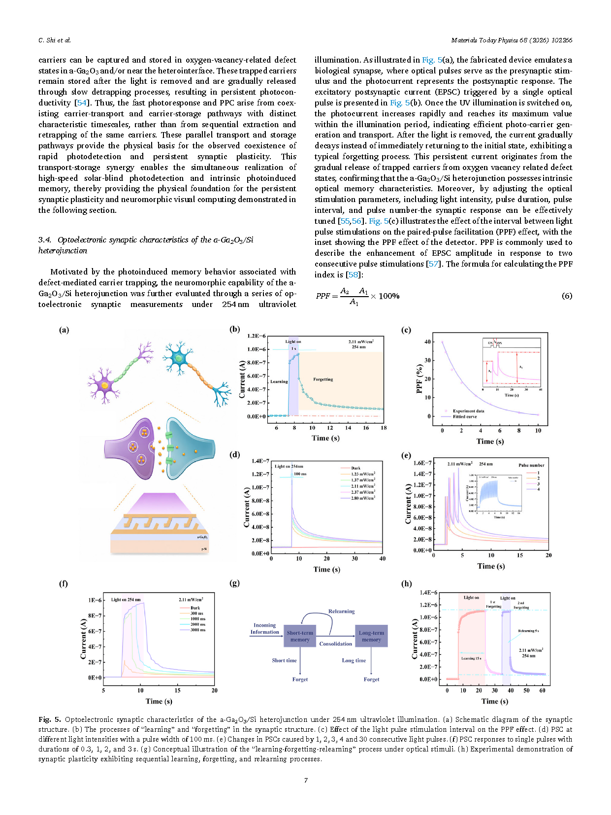
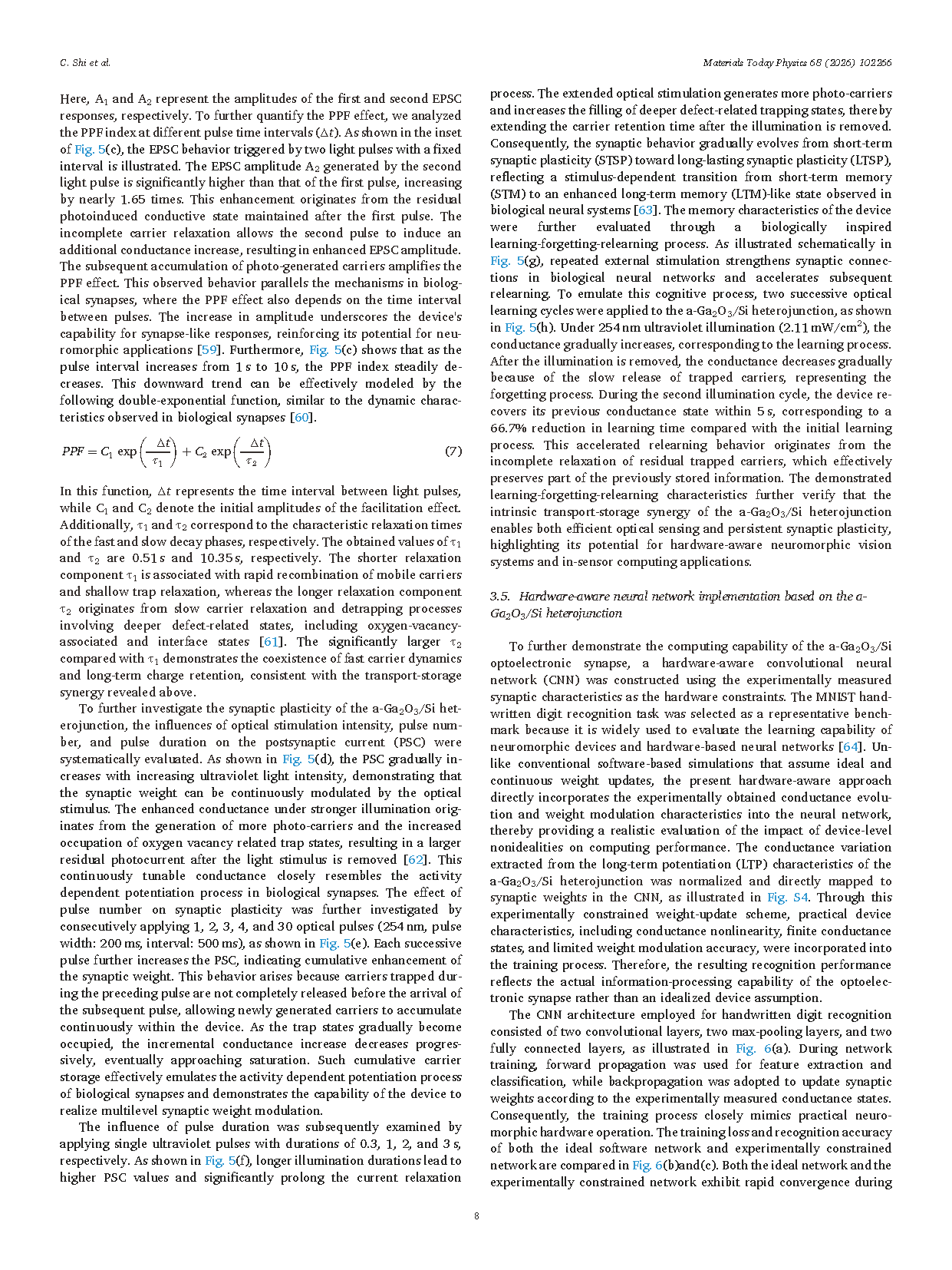
Figure 5. Optoelectronic synaptic characteristics of the a-Ga2O3/Si heterojunction under 254 nm ultraviolet illumination. (a) Schematic diagram of the synaptic structure. (b) The processes of “learning” and “forgetting” in the synaptic structure. (c) Effect of the light pulse stimulation interval on the PPF effect. (d) PSC at different light intensities with a pulse width of 100 ms. (e) Changes in PSCs caused by 1, 2, 3, 4 and 30 consecutive light pulses. (f) PSC responses to single pulses with durations of 0.3, 1, 2, and 3 s. (g) Conceptual illustration of the “learning-forgetting-relearning” process under optical stimuli. (h) Experimental demonstration of synaptic plasticity exhibiting sequential learning, forgetting, and relearning processes.
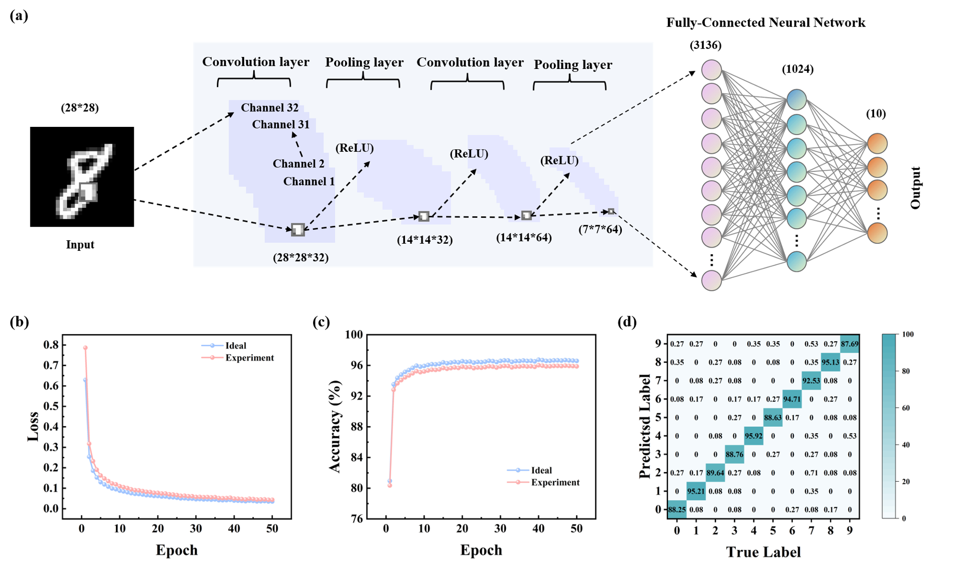
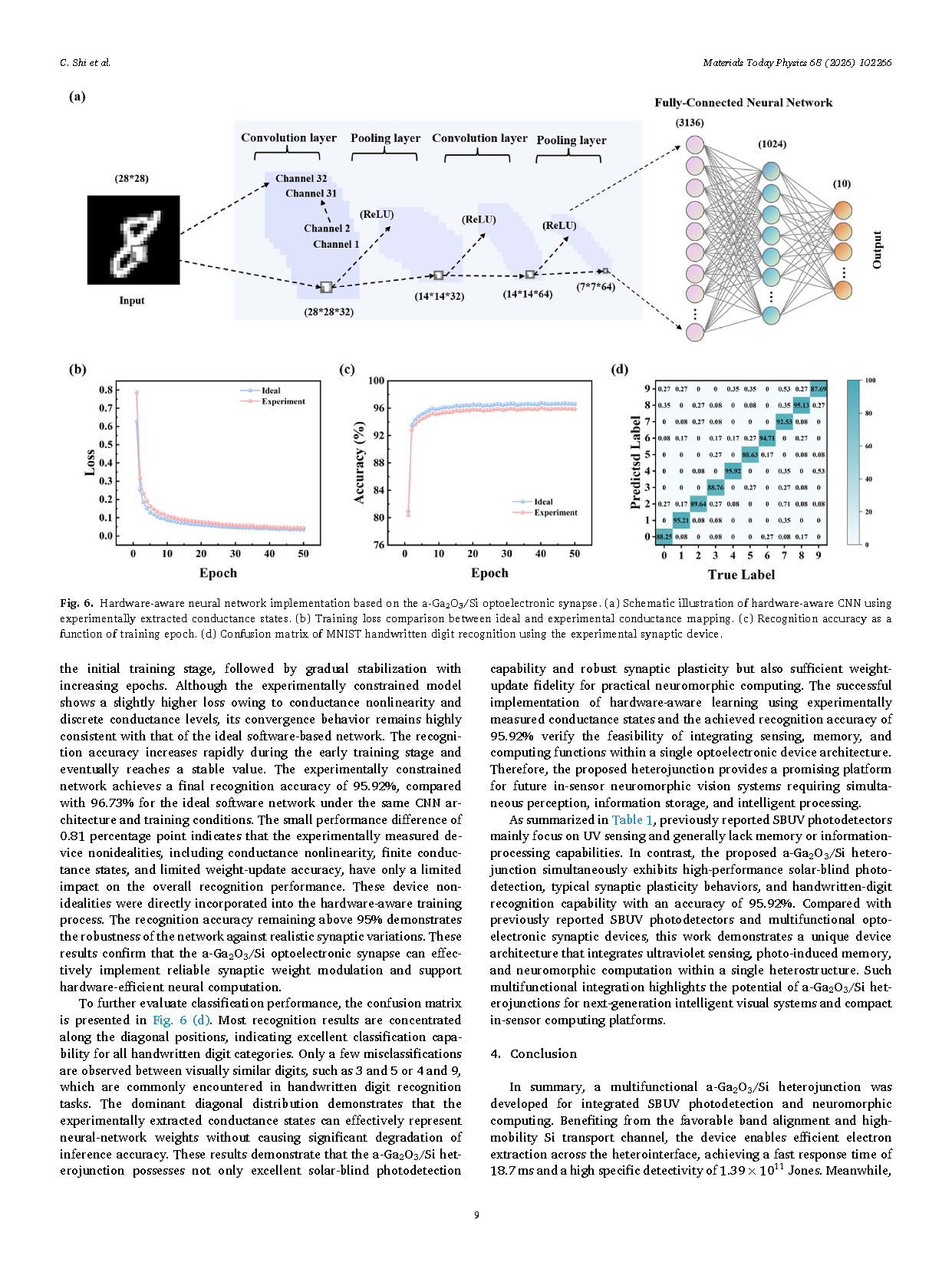
Figure 6. Hardware-aware neural network implementation based on the a-Ga2O3/Si optoelectronic synapse. (a) Schematic illustration of hardware-aware CNN using experimentally extracted conductance states. (b) Training loss comparison between ideal and experimental conductance mapping. (c) Recognition accuracy as a function of training epoch. (d) Confusion matrix of MNIST handwritten digit recognition using the experimental synaptic device.
DOI:
doi.org/10.1016/j.mtphys.2026.102266

Instruction
Official Account

Cooperation
Top
