


In March 2026, Hangzhou Garen Semiconductor Co., Ltd. (hereinafter referred to as “Garen Semiconductor”) announced the development of an 8-inch gallium oxide homoepitaxial wafer. Recently, this achievement passed a scientific and technological achievement evaluation conducted by the China Electronic Materials Industry Association (CEMIA). According to the evaluation certificate, the achievement’s key performance indicators are internationally leading, filling an international gap. It provides a foundation for research on large-diameter gallium oxide epitaxial materials and devices.
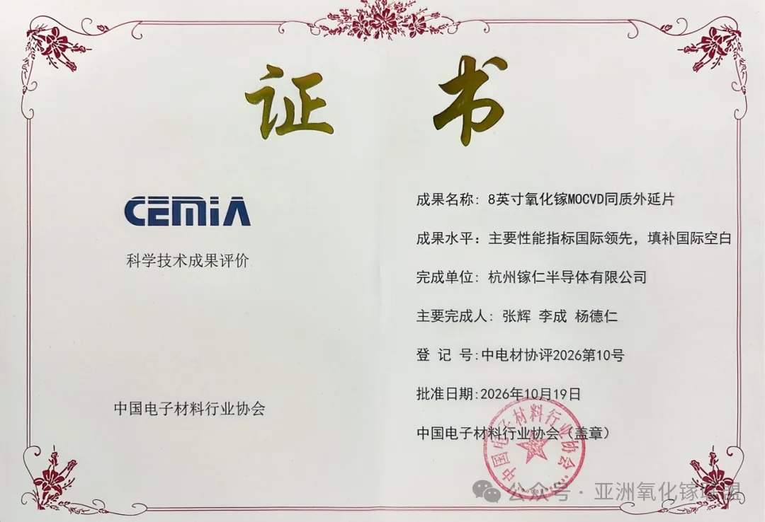
Figure 1. Scientific and Technological Achievement Evaluation Certificate
Technical Requirements for Large-Diameter Homoepitaxy
As epitaxial wafer size increases, variations in growth conditions across the wafer have a greater impact on the uniformity of film thickness, carrier concentration, and defect distribution. Therefore, evaluating the performance of an 8-inch epitaxy process requires more than simply considering wafer size; it also involves a comprehensive assessment of epitaxial uniformity, crystal quality, and electrical parameters.
Homoepitaxy involves growing an epitaxial layer of the same material on a gallium oxide substrate. This approach helps mitigate certain issues associated with lattice mismatch and thermal expansion mismatch in heteroepitaxy. However, homoepitaxy does not completely eliminate defects. Defects inherited from the substrate, as well as new defects introduced during epitaxial growth, must still be controlled through process optimization. The key to achieving 8-inch homoepitaxy lies in balancing wafer size scaling with rigorous quality control.
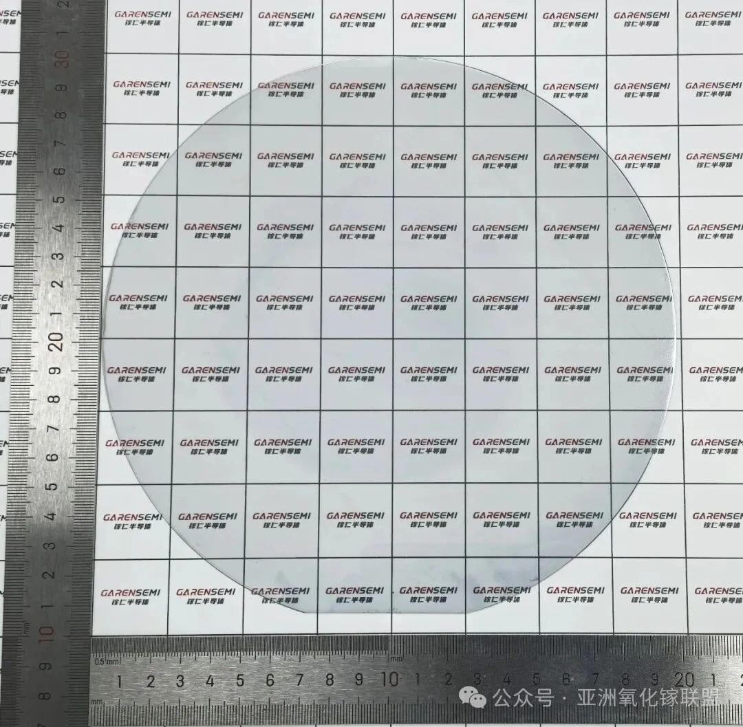
Figure 2. Garen Semiconductor’s 8-Inch Gallium Oxide Homoepitaxial Wafer
Multiple Parameters Characterize Epitaxial Quality
A previous third-party test report showed that Garen Semiconductor’s 8-inch gallium oxide homoepitaxial wafer had an average epitaxial layer thickness of 13.05 μm and a film thickness uniformity (σ) of 0.58%. The average carrier concentration of the epitaxial layer, measured using the capacitance–voltage (C–V) method, was 1.79 × 10¹⁶ cm⁻³.
X-ray diffraction (XRD) rocking curve measurements showed full widths at half maximum (FWHM) ranging from 21.1 to 46 arcsec across five measurement points. In atomic force microscopy (AFM) surface roughness measurements, the root mean square roughness (Rq) at the left and upper measurement points was 0.144 nm and 0.168 nm, respectively, while the corresponding arithmetic average roughness (Ra) was 0.115 nm and 0.134 nm, respectively.
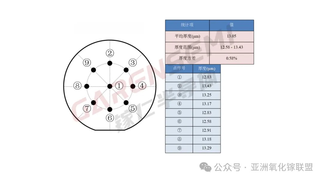
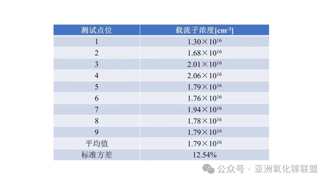
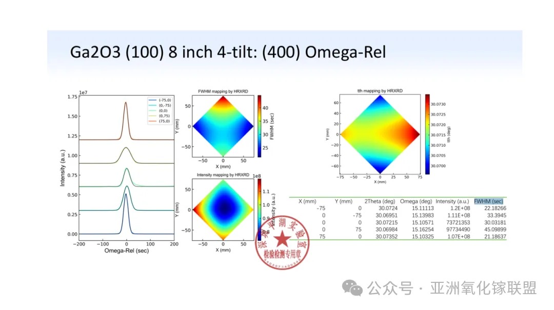
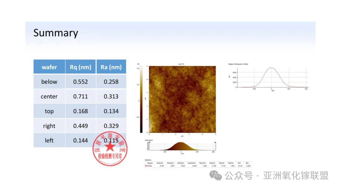
Test Results for Garen Semiconductor’s 8-Inch Gallium Oxide Homoepitaxial Wafer
The above tests characterized the epitaxial wafer in terms of film thickness, electrical properties, crystal quality, and surface morphology. The wafer achieved approximately 13 μm-thick epitaxial growth and carrier concentration control in the 1016cm-3 range on an 8-inch substrate. The overall crystal lattice exhibited an orderly arrangement, with an extremely low defect density and excellent surface flatness in the core region, meeting the standards for high-end gallium oxide epitaxial wafers.
Continued Batch Testing and Device Validation
The scientific and technological achievement evaluation assesses the progress made in research and development to date. Going forward, Garen Semiconductor will continue conducting tests across multiple batches to evaluate the stability and reproducibility of film thickness, carrier concentration, and crystal quality. The company will also advance validation of different device structures and reliability testing, while investigating the relationship between epitaxial parameters and device performance. In parallel, it will further refine testing methods and quality assessment systems to provide stable, traceable epitaxial materials for gallium oxide device research.
About Garen Semiconductor
Hangzhou Garen Semiconductor Co., Ltd. is a world-leading provider of gallium oxide materials and equipment solutions, focusing on R&D and industrial implementation for ultra-wide-bandgap semiconductors. Its core products cover: 2-inch to 12-inch gallium-oxide single crystals and substrates (world’s first constant-diameter growth for 8-inch and 12-inch specifications), gallium-oxide crystal-growth equipment adopting the Vertical Bridgman (VB) method, as well as 2-inch to 8-inch gallium-oxide homoepitaxial wafers (the 8-inch version is a world premiere). The company is committed to building a full-chain product ecosystem of "Equipment-Crystal-Substrate-Epitaxy" and delivering systematic solutions for customers worldwide. Its achievements in gallium-oxide technologies have been covered in special reports by authoritative media outlets including People’s Daily, Xinhua News Agency, Science and Technology Daily, Sina Finance, China Blue News, and The Paper.
For more information, please visit the official website: http://garen.cc/
Or contact us:
Mr. Jiang
Phone: +86 159 1871 9807
Email: jiangjiwei@garen.cc
Mr. Xia
Phone: +86 190 1127 8792
Email: xianing@garen.cc
Instruction
Official Account

Cooperation
Top