


Researchers from Seoul National University have published a dissertation titled " Charge-mediated remote epitaxy of Ga₂O₃ via MoS₂ " in Science Advances.
Background
Since the inception in 2017, remote epitaxy has emerged as a transformative growth technique, rapidly expanding from initial demonstrations on III- V arsenide and nitride materials to encompass complex oxides and other materials. This advancement has enabled novel device architectures through heterogeneous integration, showcasing the technique’s versatility and potential.
Abstract
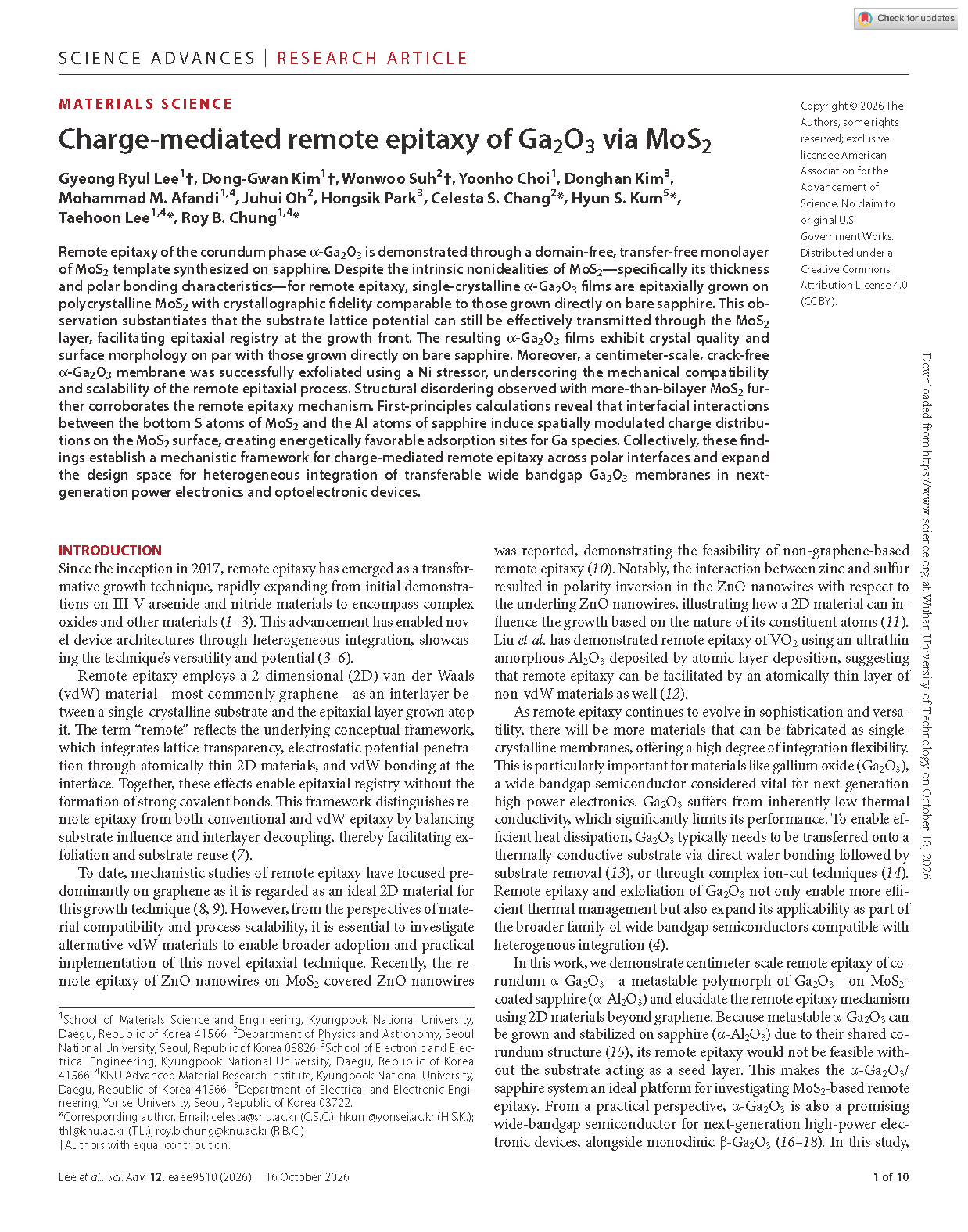
Remote epitaxy of the corundum phase α-Ga₂O₃ is demonstrated through a domain- free, transfer- free monolayer of MoS₂ template synthesized on sapphire. Despite the intrinsic nonidealities of MoS₂—specifically its thickness and polar bonding characteristics—for remote epitaxy, single-crystalline α- Ga₂O₃ films are epitaxially grown on polycrystalline MoS₂ with crystallographic fidelity comparable to those grown directly on bare sapphire. This observation substantiates that the substrate lattice potential can still be effectively transmitted through the MoS₂ layer, facilitating epitaxial registry at the growth front. The resulting α-Ga₂O₃ films exhibit crystal quality and surface morphology on par with those grown directly on bare sapphire. Moreover, a centimeter-scale, crack-free α-Ga₂O₃ membrane was successfully exfoliated using a Ni stressor, underscoring the mechanical compatibility and scalability of the remote epitaxial process. Structural disordering observed with more-than- bilayer MoS₂ further corroborates the remote epitaxy mechanism. First-principles calculations reveal that interfacial interactions between the bottom S atoms of MoS₂ and the Al atoms of sapphire induce spatially modulated charge distributions on the MoS₂ surface, creating energetically favorable adsorption sites for Ga species. Collectively, these findings establish a mechanistic framework for charge-mediated remote epitaxy across polar interfaces and expand the design space for heterogeneous integration of transferable wide bandgap Ga₂O₃ membranes in next-generation power electronics and optoelectronic devices.
Highlights
Process innovation: A solution method is employed to fabricate domain-free, large-area polycrystalline single-layer MoS₂templates on sapphire. Combined with atmospheric pressure mist CVD, centimeter-scale crack-free single-crystal α-Ga₂O₃ remote epitaxy is achieved, eliminating the need for expensive high-vacuum epitaxy equipment. However, when the number of MoS₂ layers increases to two or more, the quality of the Ga₂O₃ crystal deteriorates rapidly, and even ε-Ga₂O₃ impurities may be generated.
Proposing a new mechanism of charge-mediated long-range epitaxy: DFT first-principles calculations indicate that the interaction between Al atoms on the surface layer of sapphire and S atoms on the bottom layer of single-layer MoS₂can form spatially modulated charge depletion sites on the MoS₂ Ga atoms preferentially adsorb and nucleate at these sites, transferring the substrate crystal information to the upper film. This charge modulation effect only exists under the condition of single-layer MoS₂, explaining why polar MoS₂ can also achieve long-range epitaxy, which is different from the classical "lattice transparency" mechanism of graphene.
Thin Film Performance and Peeling Verification: The quality and surface morphology of α-Ga₂O₃crystals grown on a single layer of MoS₂ are comparable to those grown directly on sapphire. The interface undergoes stress relaxation due to van der Waals interactions, resulting in almost no residual strain. With the help of a Ni stress layer, complete mechanical peeling of centimeter-scale α-Ga₂O₃ films is achieved, yielding transferable self-supporting gallium oxide single crystal films. The substrate can be reused, facilitating subsequent hetero-integration and thermal management optimization.
Mechanism corroboration experiment: Oxygen plasma treatment of sapphire induces S-O covalent bonding, which completely inhibits the nucleation and growth of α-Ga₂O₃. This indirectly confirms that the interface charge effect is the core of remote epitaxy in this system, providing a theoretical framework and new ideas for the design of remote epitaxial materials for other polar interfaces.
Conclusion
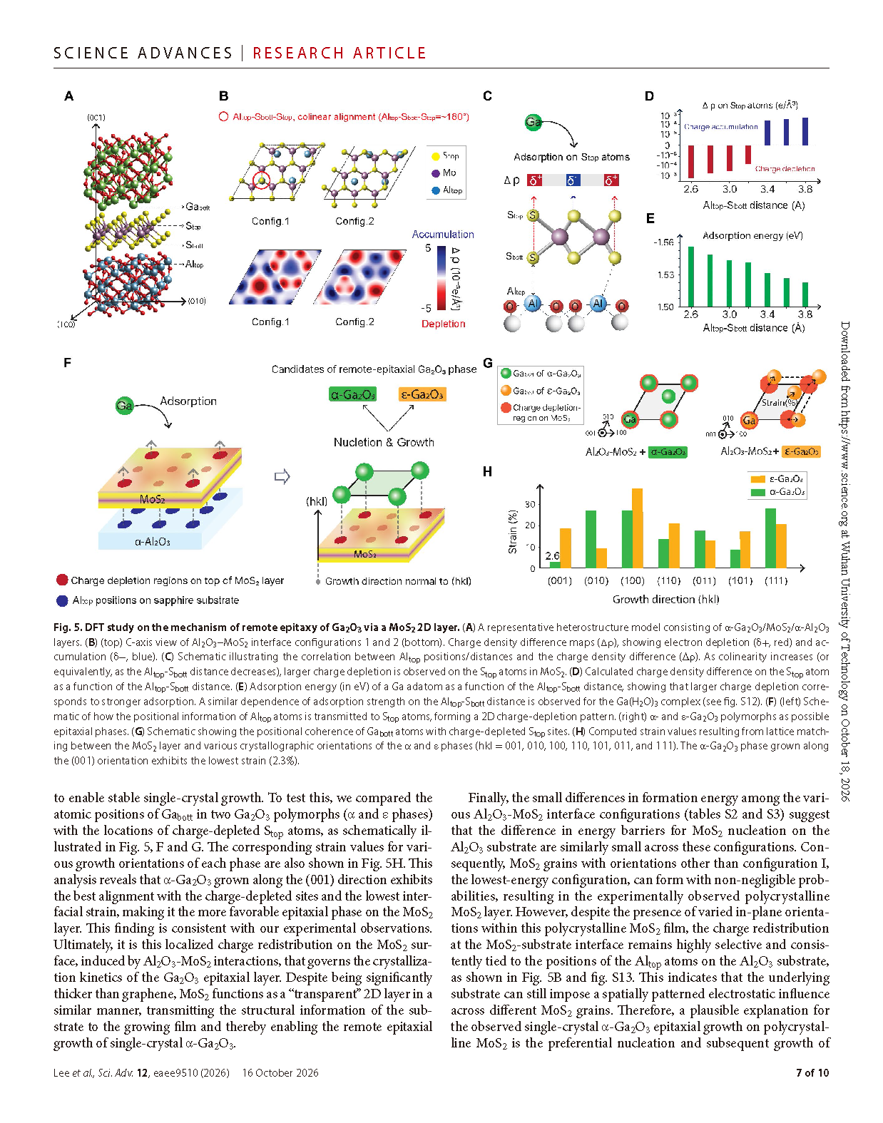
Finally, the small differences in formation energy among the various Al₂O₃-MoS₂ interface configurations (tables S2 and S3) suggest that the difference in energy barriers for MoS₂ nucleation on the Al₂O₃ substrate are similarly small across these configurations. Consequently, MoS₂ grains with orientations other than configuration I, the lowest-energy configuration, can form with non-negligible prob abilities, resulting in the experimentally observed polycrystalline MoS₂ layer. However, despite the presence of varied in-plane orientations within this polycrystalline MoS₂ film, the charge redistribution at the MoS₂-substrate interface remains highly selective and consistently tied to the positions of the Altop atoms on the Al₂O₃ substrate, as shown in Fig. 5B and fig. S13. This indicates that the underlying substrate can still impose a spatially patterned electrostatic influence across different MoS₂ grains. Therefore, a plausible explanation for the observed single-crystal α-Ga₂O₃ epitaxial growth on polycrystal line MoS₂ is the preferential nucleation and subsequent growth of Ga₂O₃ at these substrate-imprinted, charge-depleted sites, regardless of the grain orientation of the underlying MoS₂.
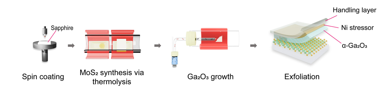
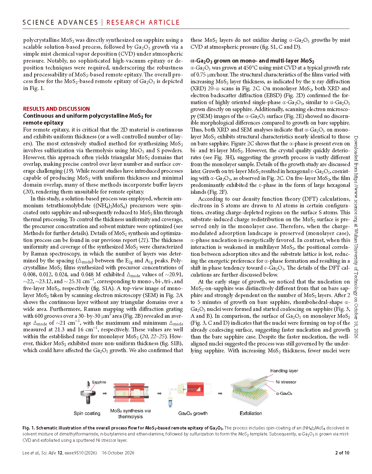
Fig. 1. Schematic illustration of the overall process flow for MoS₂-based remote epitaxy of Ga₂O₃. the process includes spin-coating of an (NH₄)₂MoS₄ dissolved in solvent mixture of dimethylformamide, n-butylamine and ethanolamine, followed by sulfurization to form the MoS₂ template. Subsequently, α-Ga₂O₃ is grown via mist-CVD and exfoliated using a sputtered Ni stressor layer.
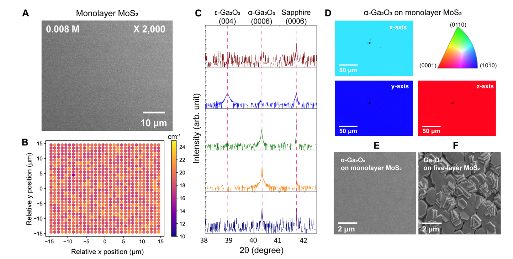
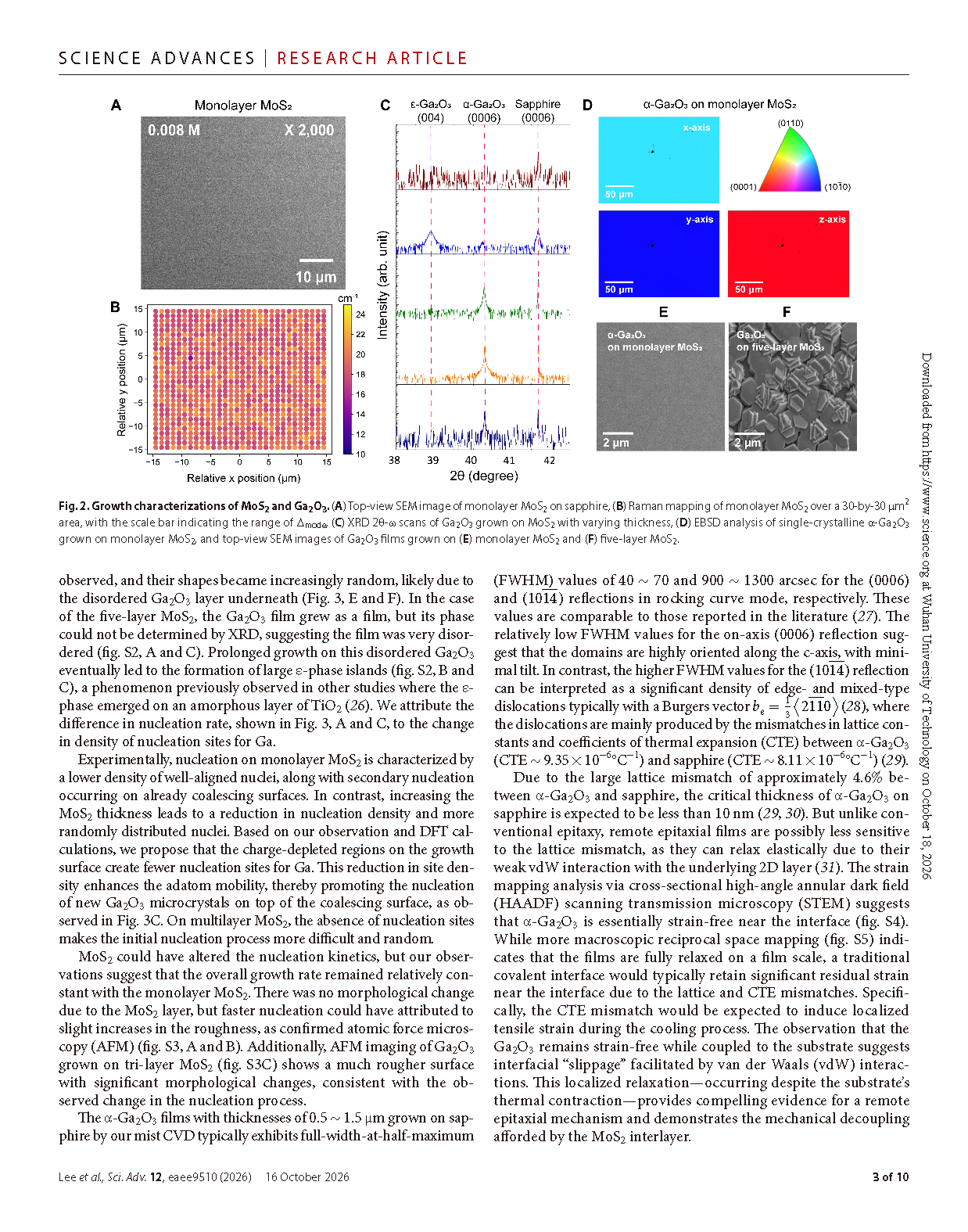
Fig. 2. Growth characterizations of MoS₂ and Ga₂O₃. (A) top-view SeM image of monolayer MoS₂ on sapphire, (B) Raman mapping of monolayer MoS₂ over a 30-by-30 μm2 area, with the scale bar indicating the range of ∆mode, (C) XRD 2θ-ω scans of Ga₂O₃ grown on MoS₂ with varying thickness, (D) EBSD analysis of single-crystalline α-Ga₂O₃ grown on monolayer MoS₂, and top-view SeM images of Ga₂O₃ films grown on (E) monolayer MoS₂ and (F) five-layer MoS₂.
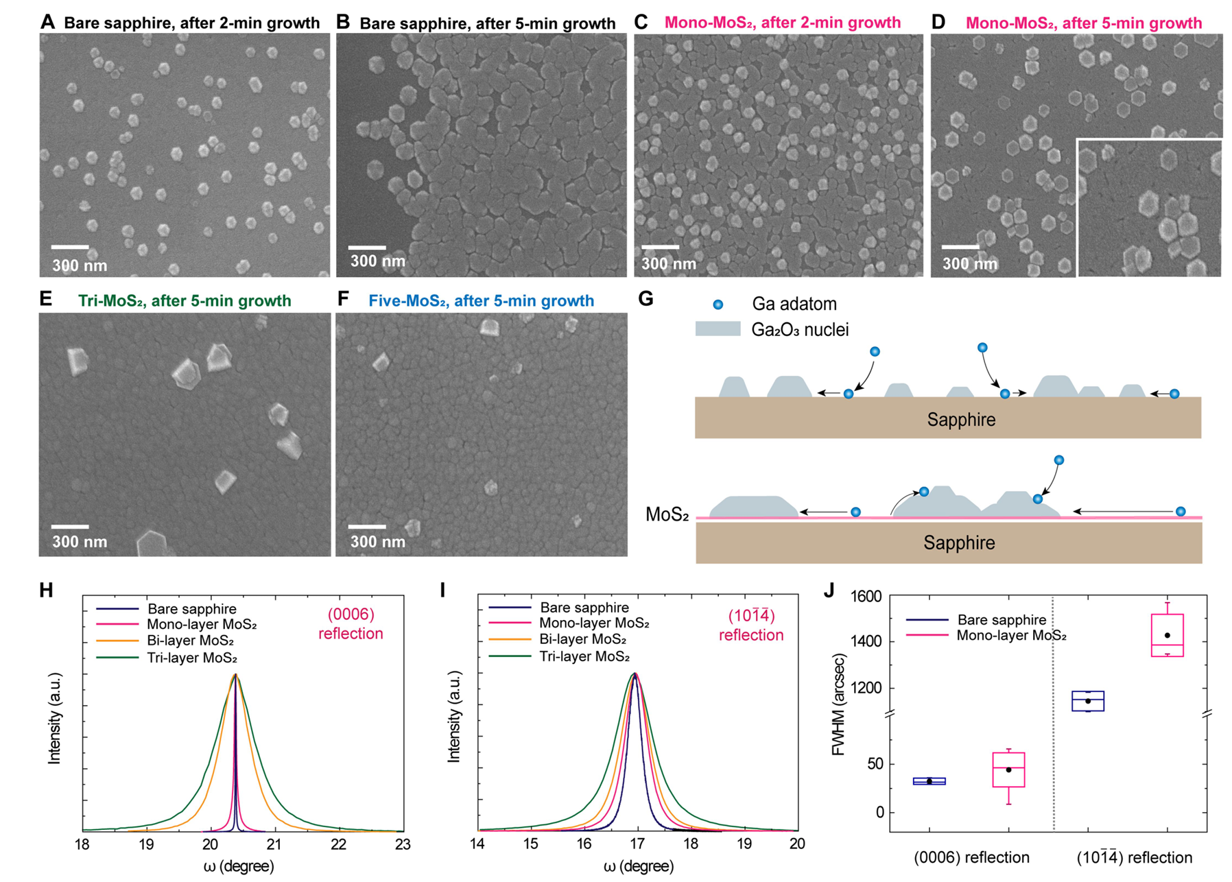
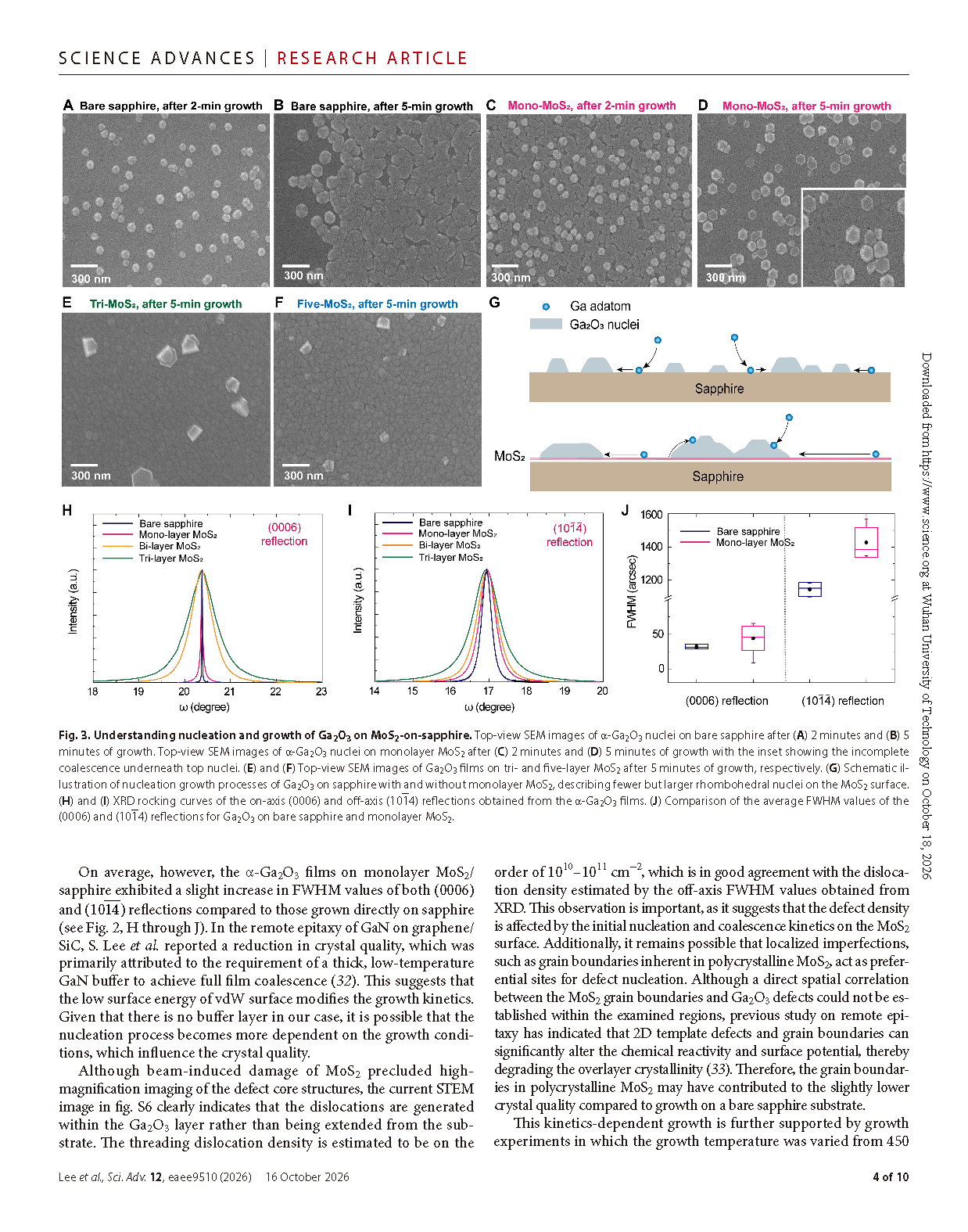
Fig. 3. Understanding nucleation and growth of Ga₂O₃ on MoS₂-on-sapphire. top-view SEM images of α-Ga₂O₃ nuclei on bare sapphire after (A) 2 minutes and (B) 5 minutes of growth. top-view SEM images of α-Ga₂O₃ nuclei on monolayer MoS₂ after (C) 2 minutes and (D) 5 minutes of growth with the inset showing the incomplete coalescence underneath top nuclei. (E) and (F) top- view SEM images of Ga₂O₃ films on tri-and five-layer MoS₂ after 5 minutes of growth, respectively. (G) Schematic il lustration of nucleation growth processes of Ga₂O₃ on sapphire with and without monolayer MoS₂, describing fewer but larger rhombohedral nuclei on the MoS₂ surface. (H) and (I) XRD rocking curves of the on-axis (0006) and off-axis (10-14) reflections obtained from the α-Ga₂O₃ films. (J) comparison of the average FWHM values of the (0006) and (10-14) reflections for Ga₂O₃ on bare sapphire and monolayer MoS₂.
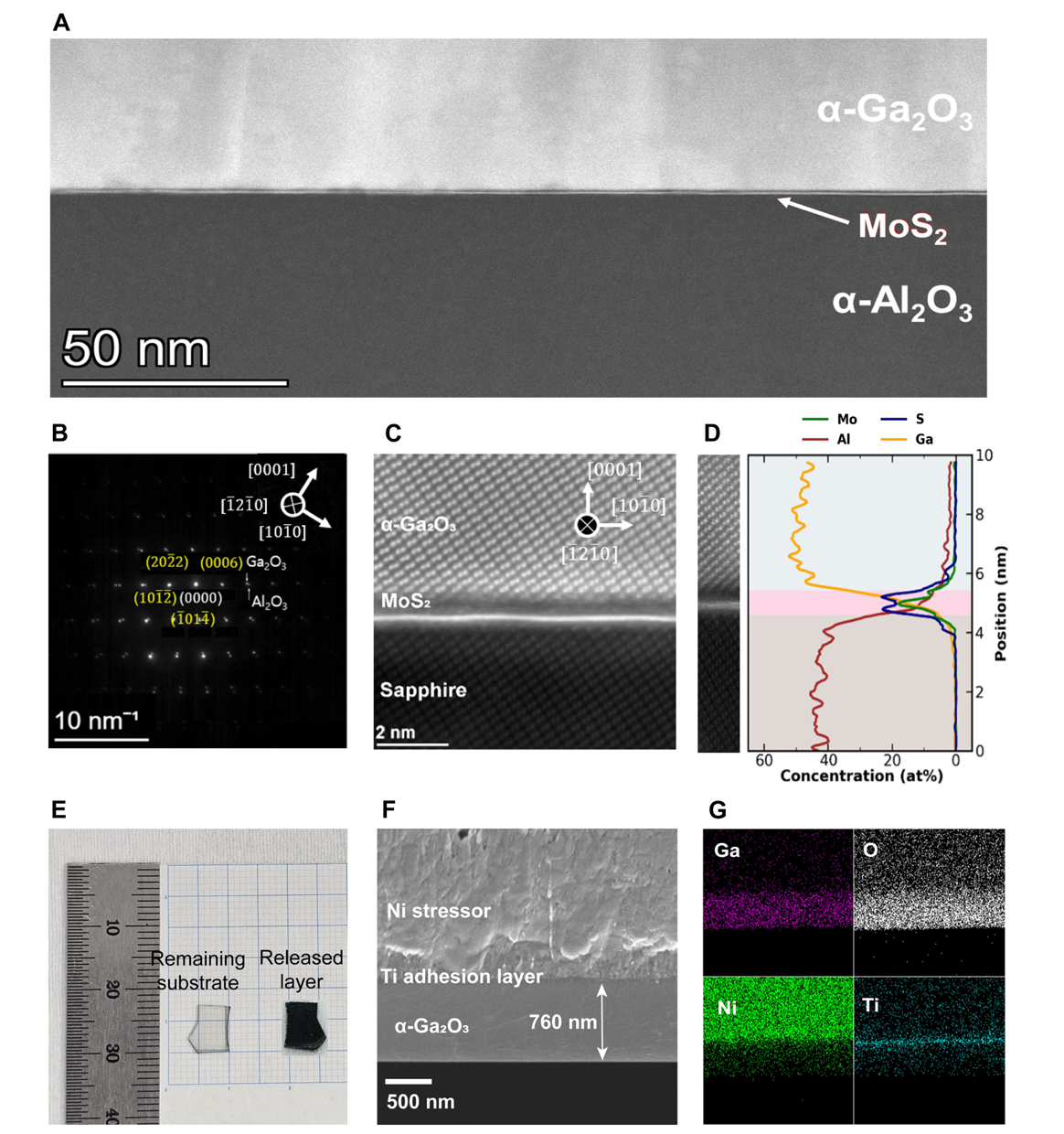
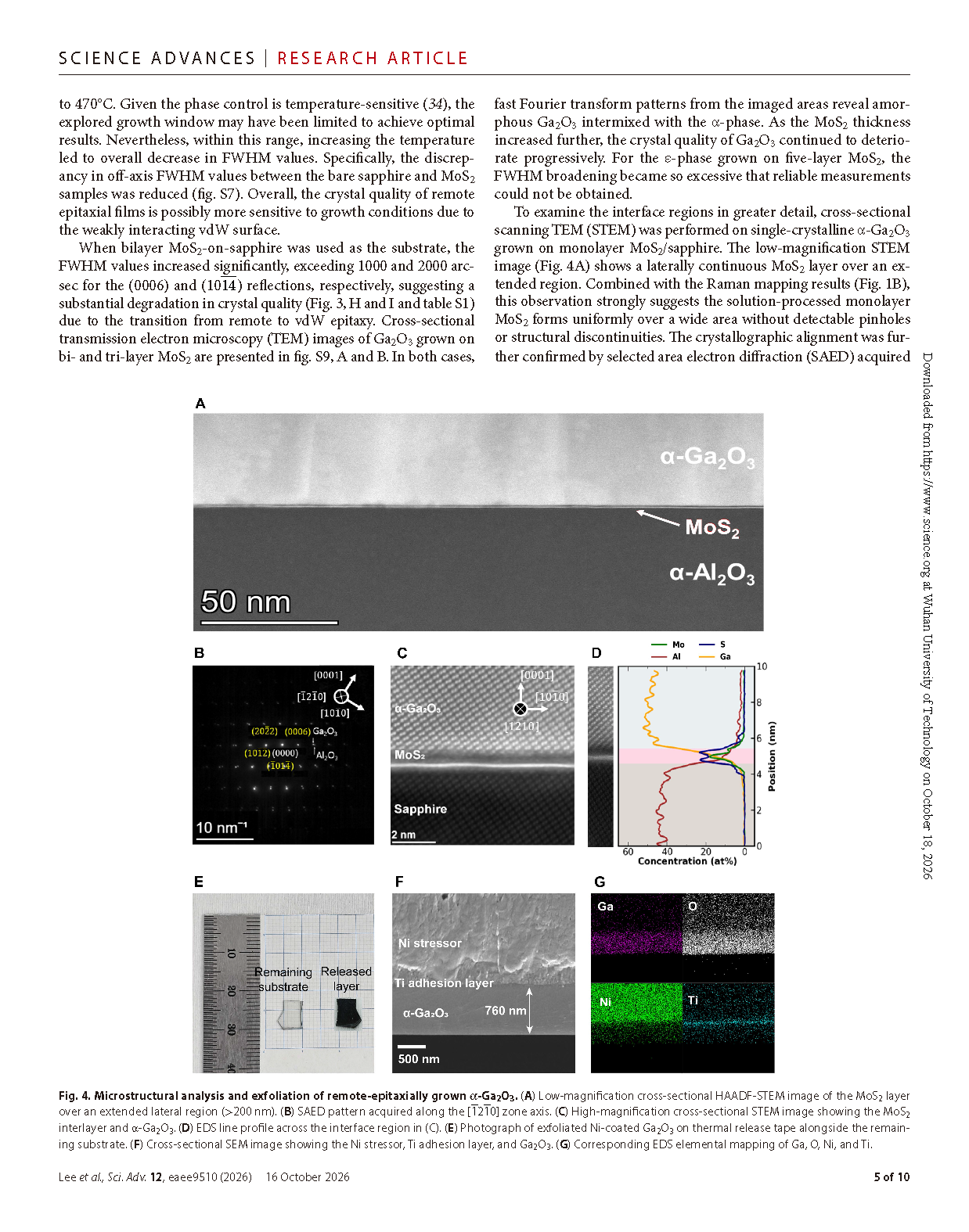
Fig. 4. Microstructural analysis and exfoliation of remote-epitaxially grown α-Ga₂O₃. (A) Low-magnification cross-sectional HAADF-STEM image of the MoS₂ layer over an extended lateral region (>200 nm). (B) SAED pattern acquired along the [-12-10] zone axis. (C) high-magnification cross-sectional STEM image showing the MoS₂ interlayer and α-Ga₂O₃. (D) EDS line profile across the interface region in (c). (E) Photograph of exfoliated Ni-coated Ga₂O₃ on thermal release tape alongside the remaining substrate. (F) cross- sectional SEM image showing the Ni stressor, Ti adhesion layer, and Ga₂O₃. (G) corresponding EDS elemental mapping of Ga, O, Ni, and Ti.
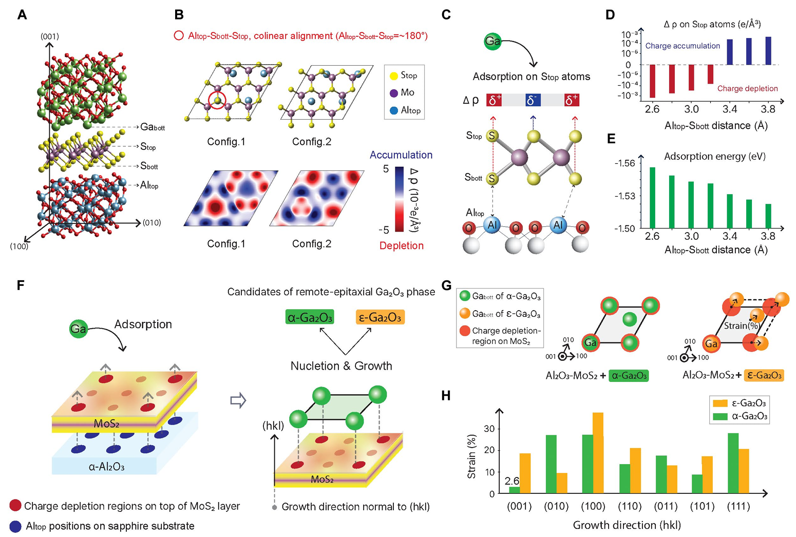
Fig. 5. DFT study on the mechanism of remote epitaxy of Ga₂O₃ via a MoS₂ 2D layer. (A) A representative heterostructure model consisting of α-Ga₂O₃/MoS₂/α-Al₂O₃ layers. (B) (top) c-axis view of Al₂O₃–MoS₂ interface configurations 1 and 2 (bottom). charge density difference maps (Δρ), showing electron depletion (δ+, red) and ac cumulation (δ−, blue). (C) Schematic illustrating the correlation between Altop positions/distances and the charge density difference (Δρ). As colinearity increases (or equivalently, as the Altop- Sbott distance decreases), larger charge depletion is observed on the Stop atoms in MoS₂. (D) calculated charge density difference on the Stop atom as a function of the Altop-Sbott distance. (E) Adsorption energy (in eV) of a Ga adatom as a function of the Altop-Sbott distance, showing that larger charge depletion corresponds to stronger adsorption. A similar dependence of adsorption strength on the Altop-Sbott distance is observed for the Ga(h2O)3 complex (see fig. S12). (F) (left) Schematic of how the positional information of Altop atoms is transmitted to Stop atoms, forming a 2d charge-depletion pattern. (right) α-and ε-Ga₂O₃ polymorphs as possible epitaxial phases. (G) Schematic showing the positional coherence of Gabott atoms with charge-depleted Stop sites. (H) computed strain values resulting from lattice matching between the MoS₂ layer and various crystallographic orientations of the α and ε phases (hkl=001, 010, 100, 110, 101, 011, and 111). the α-Ga₂O₃ phase grown along the (001) orientation exhibits the lowest strain (2.3%).
DOI:
10.1126/sciadv.aee9510
Instruction
Official Account

Cooperation
Top
