


Researchers from Novel Crystal Technology have published a dissertation titled "Growth of 2-inch n-type β-Ga₂O₃ (011) single crystal by vertical Bridgman method" in Japanese Journal of Applied Physics.
Background
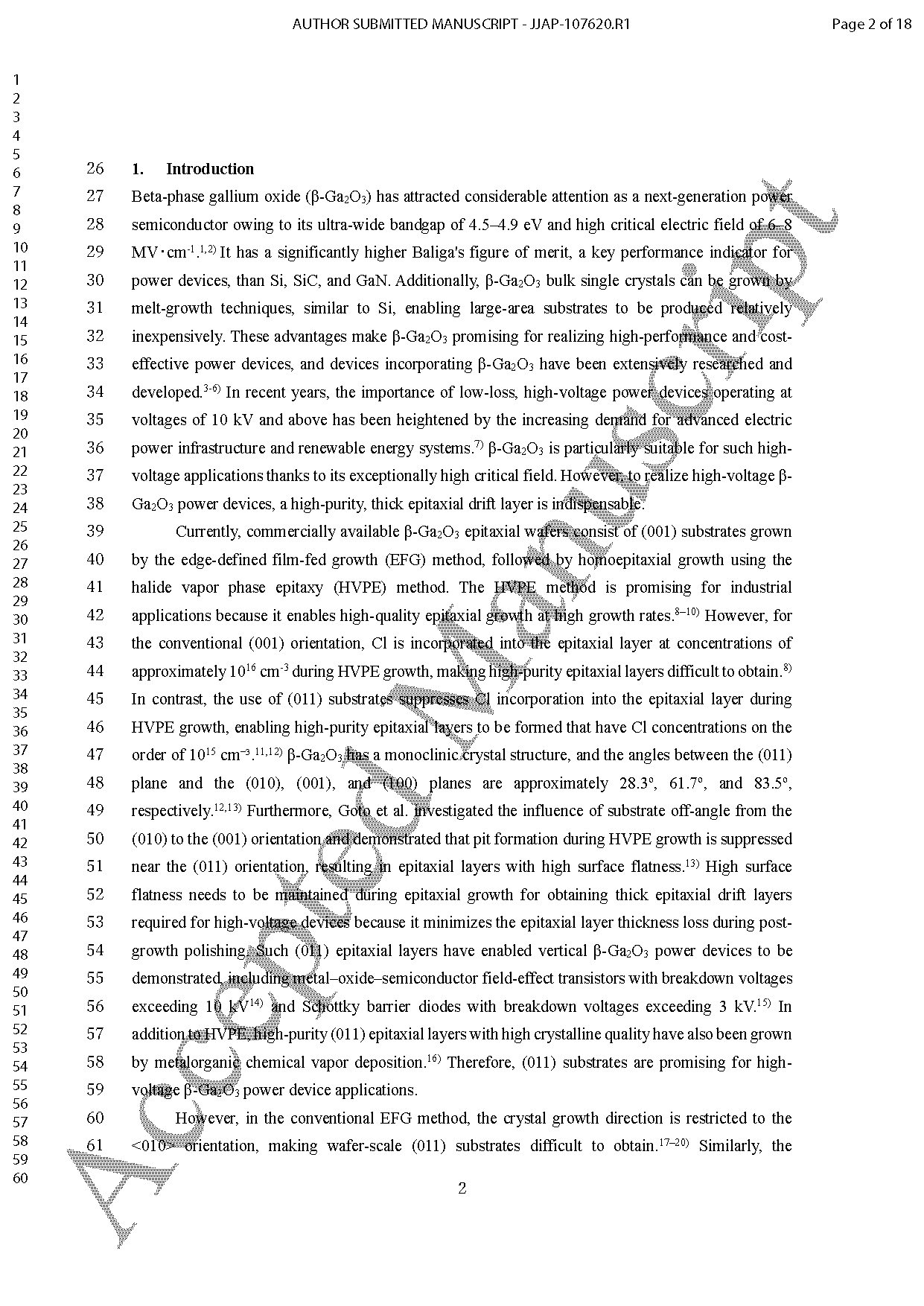
β-Ga₂O₃ is an important candidate for high-voltage power semiconductors owing to its ultra-wide bandgap and extremely high theoretical breakdown field. It possesses much higher Baliga's figure-of-merit than Si, SiC and GaN. Bulk single crystals can be obtained via melt-growth techniques, which is suitable for low-cost high-power device fabrication. For high-voltage power equipment above 10 kV, high-purity thick drift epitaxial layers are required. The (011)-oriented substrate can suppress Cl impurity incorporation during HVPE epitaxy and avoid pit defects on epitaxial surfaces, making it a promising substrate for high-voltage devices. Nevertheless, mainstream melt-growth techniques such as EFG, CZ and casting are restricted by crystal growth orientation, and it is difficult to directly fabricate wafer-scale (011) β-Ga₂O₃ single-crystal substrates. The vertical Bridgman method has realized large-size β-Ga₂O₃ single crystals of (100), (010) and (001) orientations. However, whether 2-inch single crystals can be grown along the normal direction of (011), as well as its crystal quality and electrical uniformity, have not been verified, which restricts further development of (011)-based Ga₂O₃ power devices.
Abstract
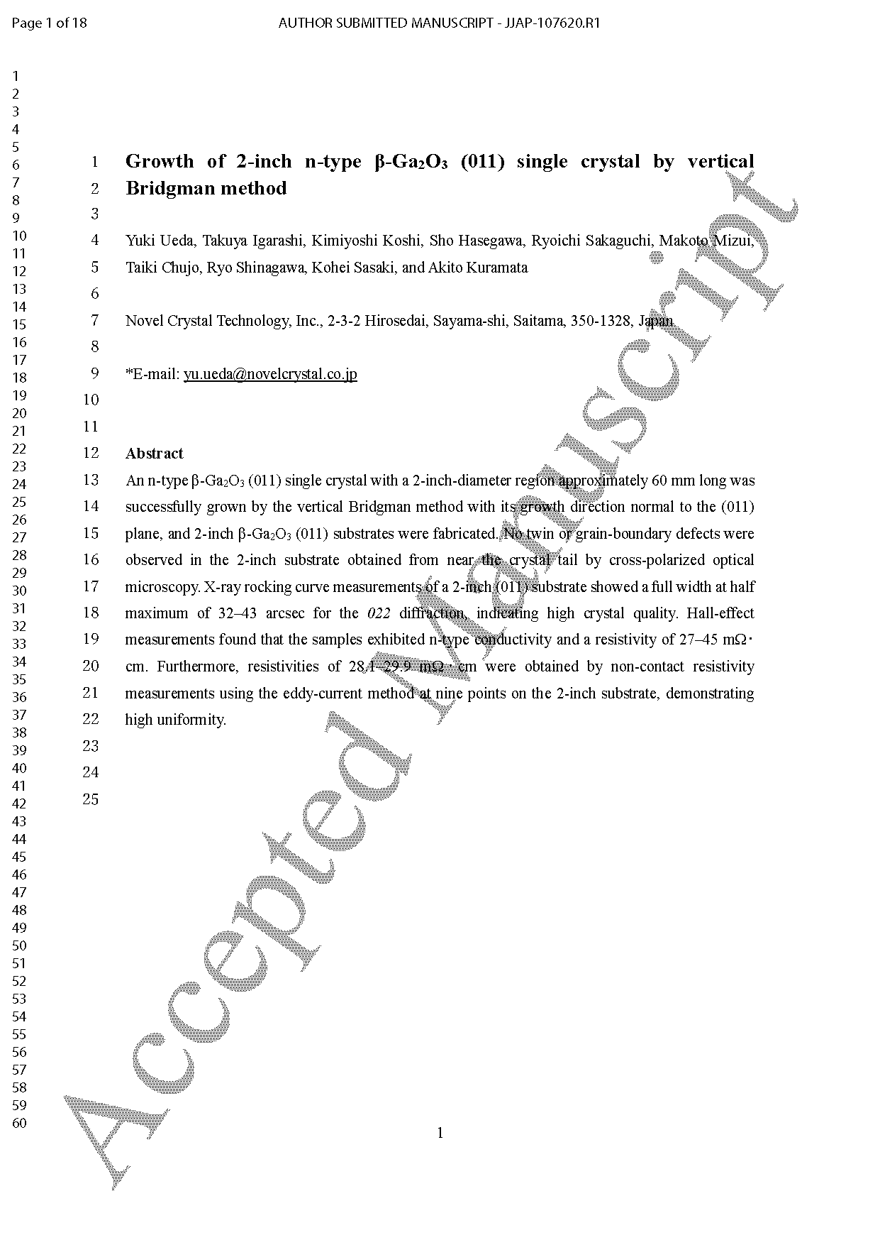
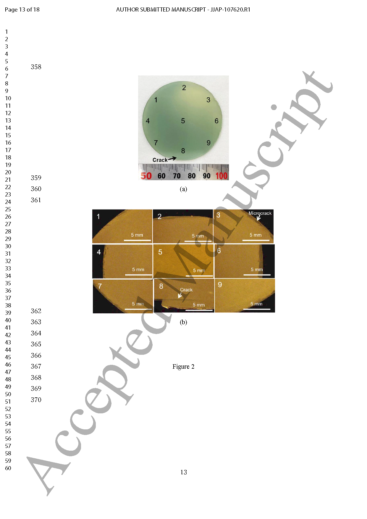
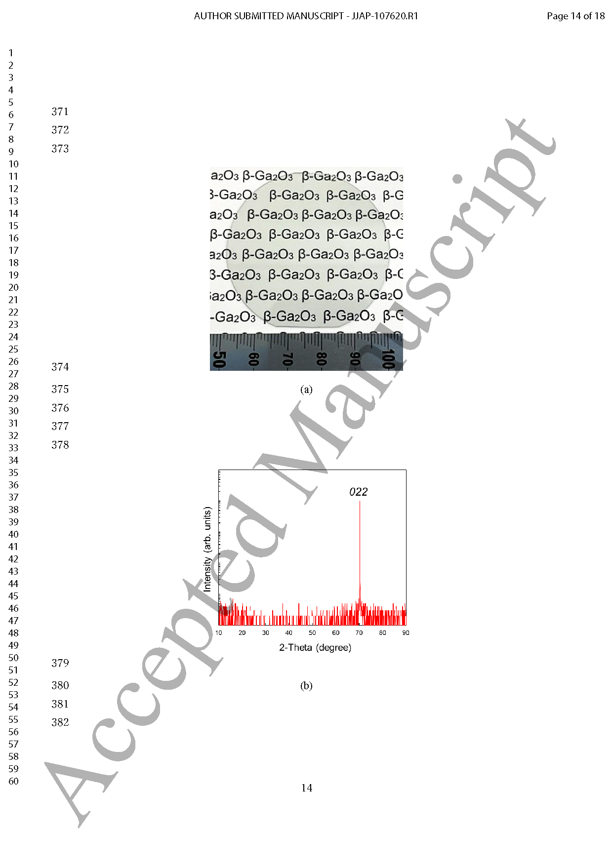
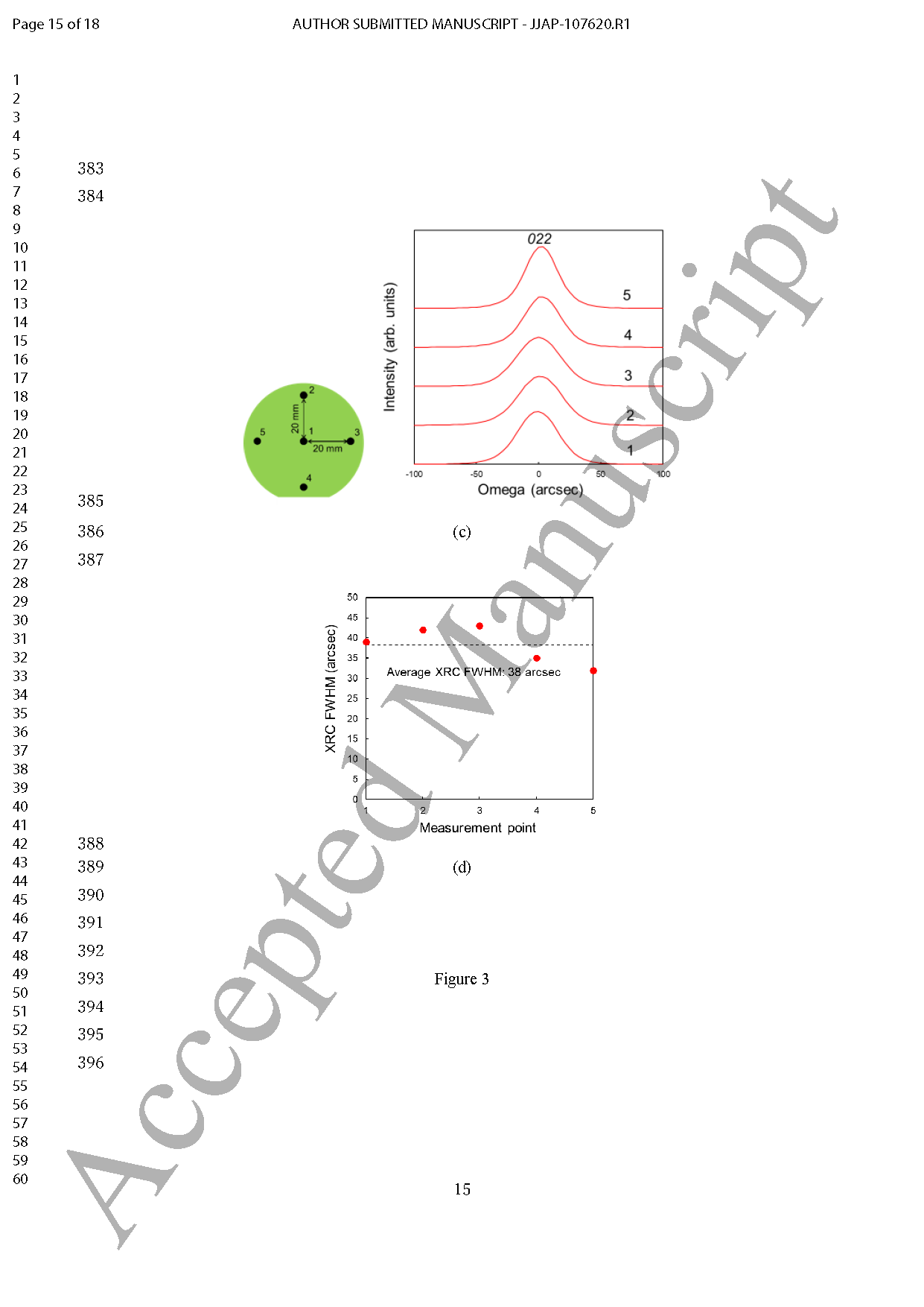
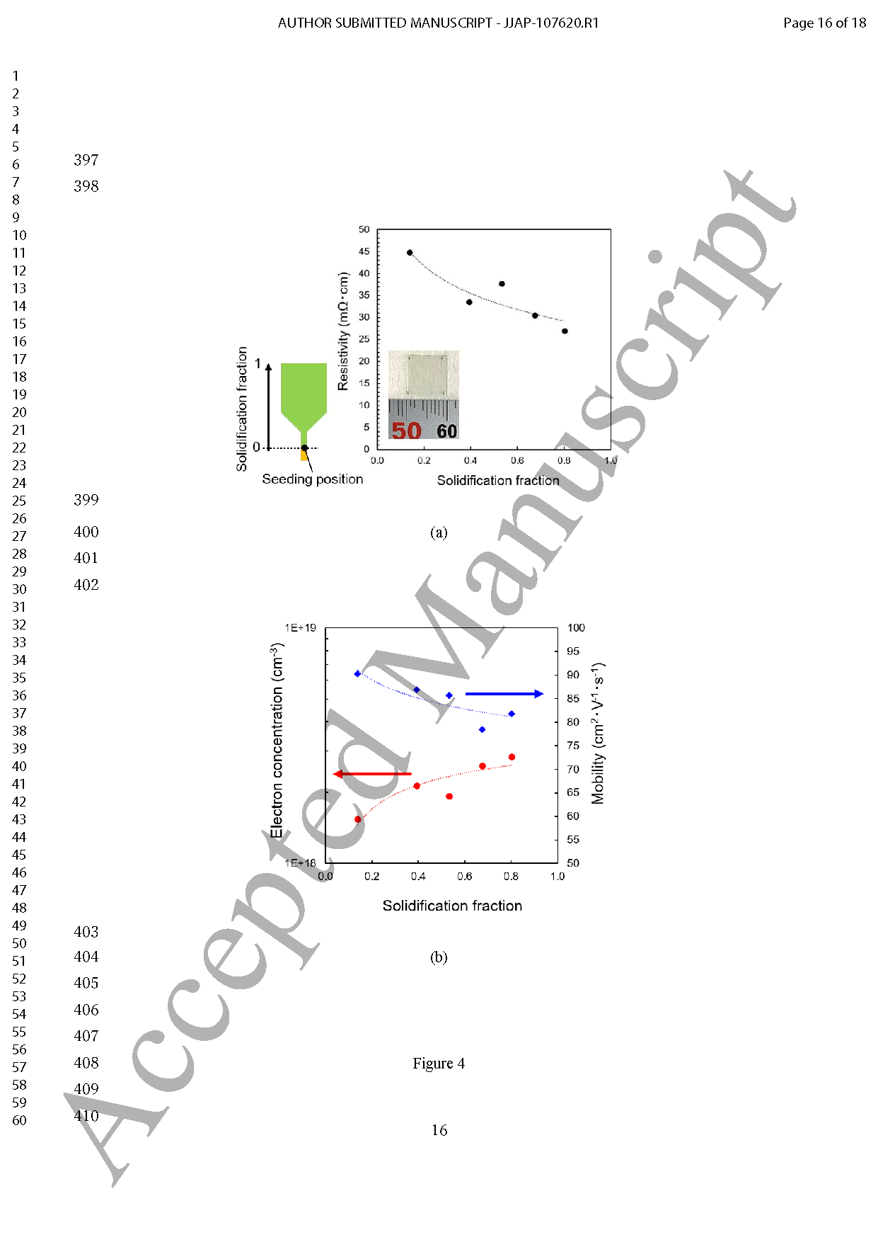
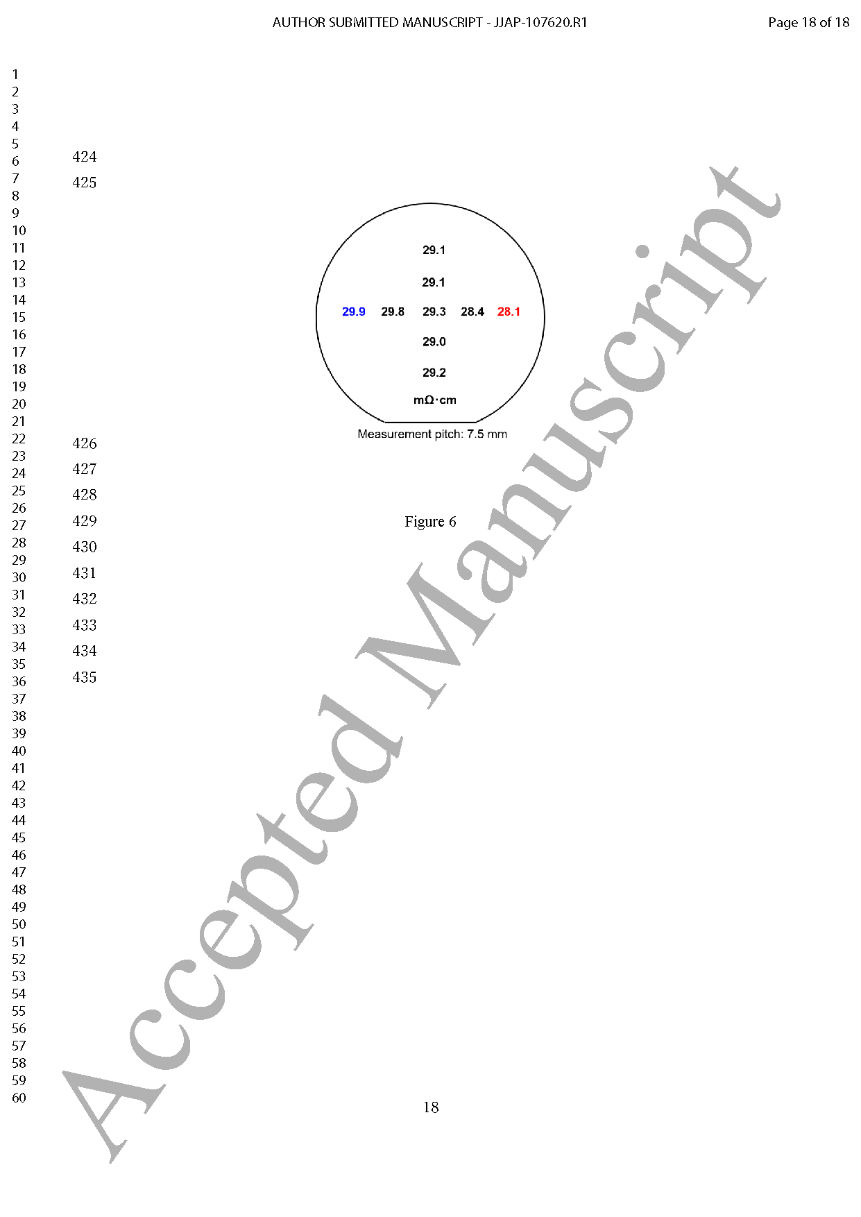
An n-type β-Ga₂O₃ (011) single crystal with a 2-inch-diameter region approximately 60 mm long was successfully grown by the vertical Bridgman method with its growth direction normal to the (011) plane, and 2-inch β-Ga₂O₃ (011) substrates were fabricated. No twin or grain-boundary defects were observed in the 2-inch substrate obtained from near the crystal tail by cross-polarized optical microscopy. X-ray rocking curve measurements of a 2-inch (011) substrate showed a full width at half maximum of 32–43 arcsec for the 022 diffraction, indicating high crystal quality. Hall-effect measurements found that the samples exhibited n-type conductivity and a resistivity of 27–45 mΩ·cm. Furthermore, resistivities of 28.1–29.9 mΩ·cm were obtained by non-contact resistivity measurements using the eddy-current method at nine points on the 2-inch substrate, demonstrating high uniformity.
Highlights
Realize 2-inch n-type β-Ga₂O₃(011) single-crystal growth with growth direction normal to (011) plane by vertical Bridgman method, and fabricate corresponding substrates.
Near-tail substrate is free of twin and grain-boundary defects, and 022 rocking-curve FWHM reaches 32-43 arcsec with high crystalline quality.
Obtain n-type conductive substrates with resistivity of 27-45 mΩ·cm; eddy-current test shows excellent in-plane electrical uniformity across 2-inch wafer.
Demonstrate orientation flexibility of vertical Bridgman method for β-Ga₂O₃ bulk crystal, providing new route for (011) large-area substrate manufacturing.
Conclusion
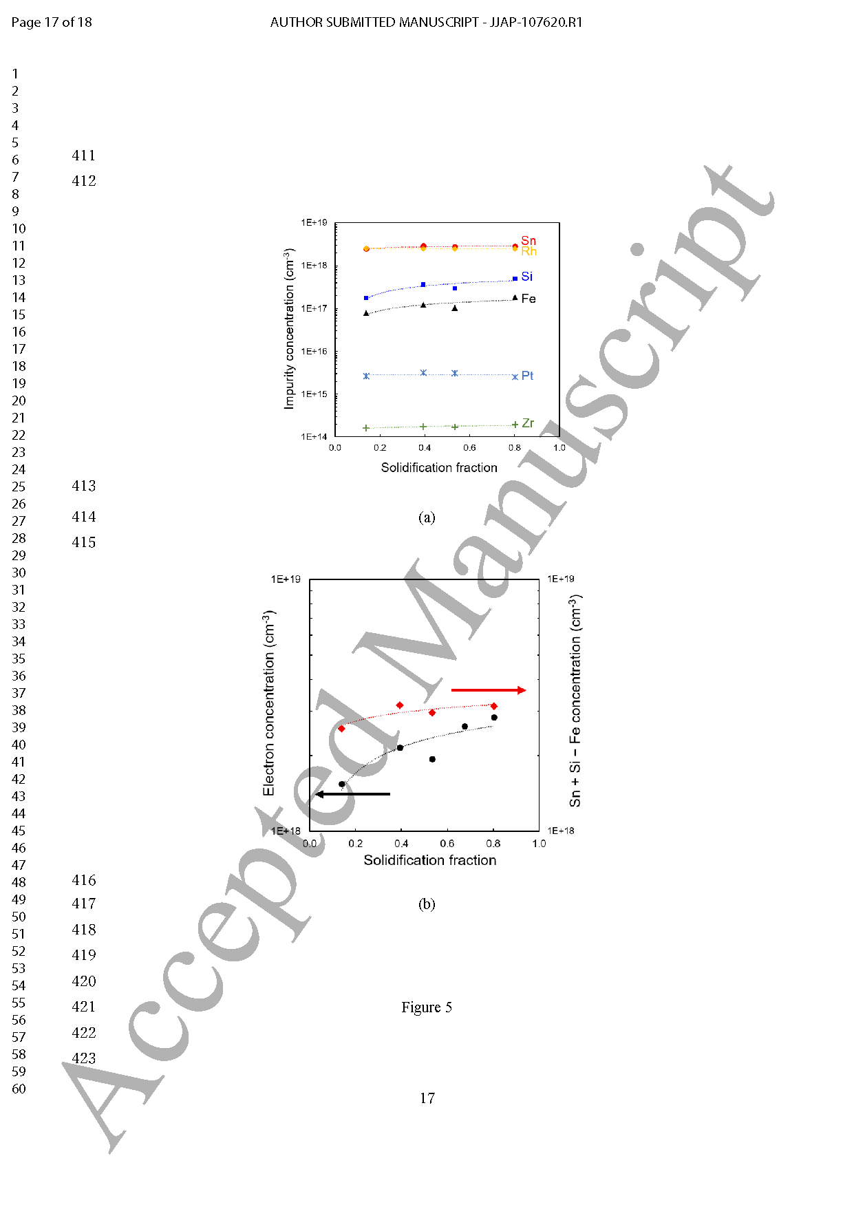
An n-type β-Ga₂O₃ (011) single crystal with a 2-inch-diameter region approximately 60 mm long was successfully grown by the resistance-heated vertical Bridgman (VB) method with its growth direction normal to the (011) plane using a Pt–Rh alloy crucible. Additionally, 2-inch β-Ga₂O₃ (011) substrates were successfully fabricated from the grown crystal. No twin or grain-boundary defects were observed in the 2-inch substrate obtained from near the crystal tail by cross-polarized optical microscopy. Rocking curve (XRC) measurements of a 2-inch (011) substrate after chemical-mechanical polishing (CMP) showed a full width at half maximum (FWHM) of 32–43 arcsec for the 022 diffraction, indicating high crystal quality. Hall-effect measurements found that the samples exhibited n-type conductivity and a resistivity of 27–45 mΩ·cm. The electron concentration and mobility were 1.5 × 10¹⁸-2.8 × 10¹⁸ cm⁻³ and 78-90 cm²·V⁻¹·s⁻¹. The electron concentration increased as the solidification fraction of the melt increased. For the sample corresponding to the melt solidification fraction of 0.8, the electron concentration measured by Hall-effect measurements agreed well with that estimated from the concentrations of the electrically active impurities (Sn, Si, and Fe) determined by secondary ion mass spectrometry (SIMS). Furthermore, resistivities of 28.1–29.9 mΩ·cm were obtained by noncontact resistivity measurements using the eddy-current method at nine points on the 2-inch substrate, demonstrating high uniformity. These results suggest that the solid-liquid interface was nearly flat during crystal growth and that the impurity concentration was highly uniform across the growth cross section. Further investigation is required, however, to elucidate the actual crystal growth behavior during crucible descent. The demonstration of wafer-scale β-Ga₂O₃ (011) substrates grown by the VB method is expected to accelerate the development of high-voltage β-Ga₂O₃ power devices.
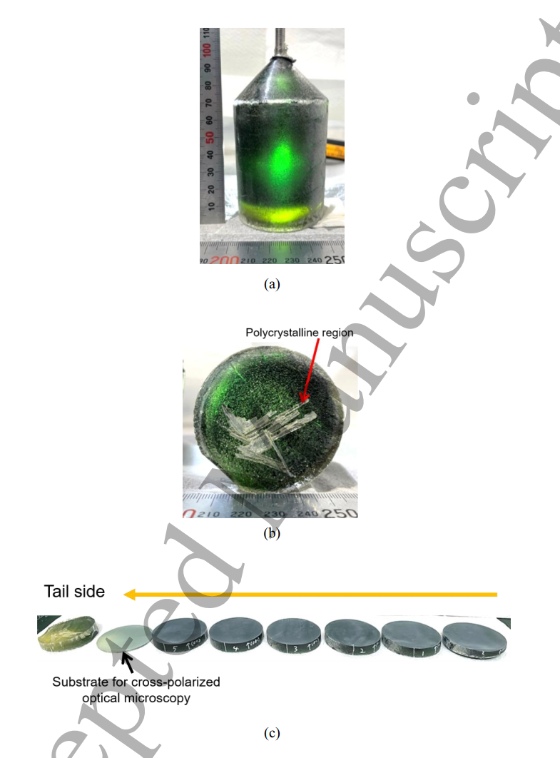
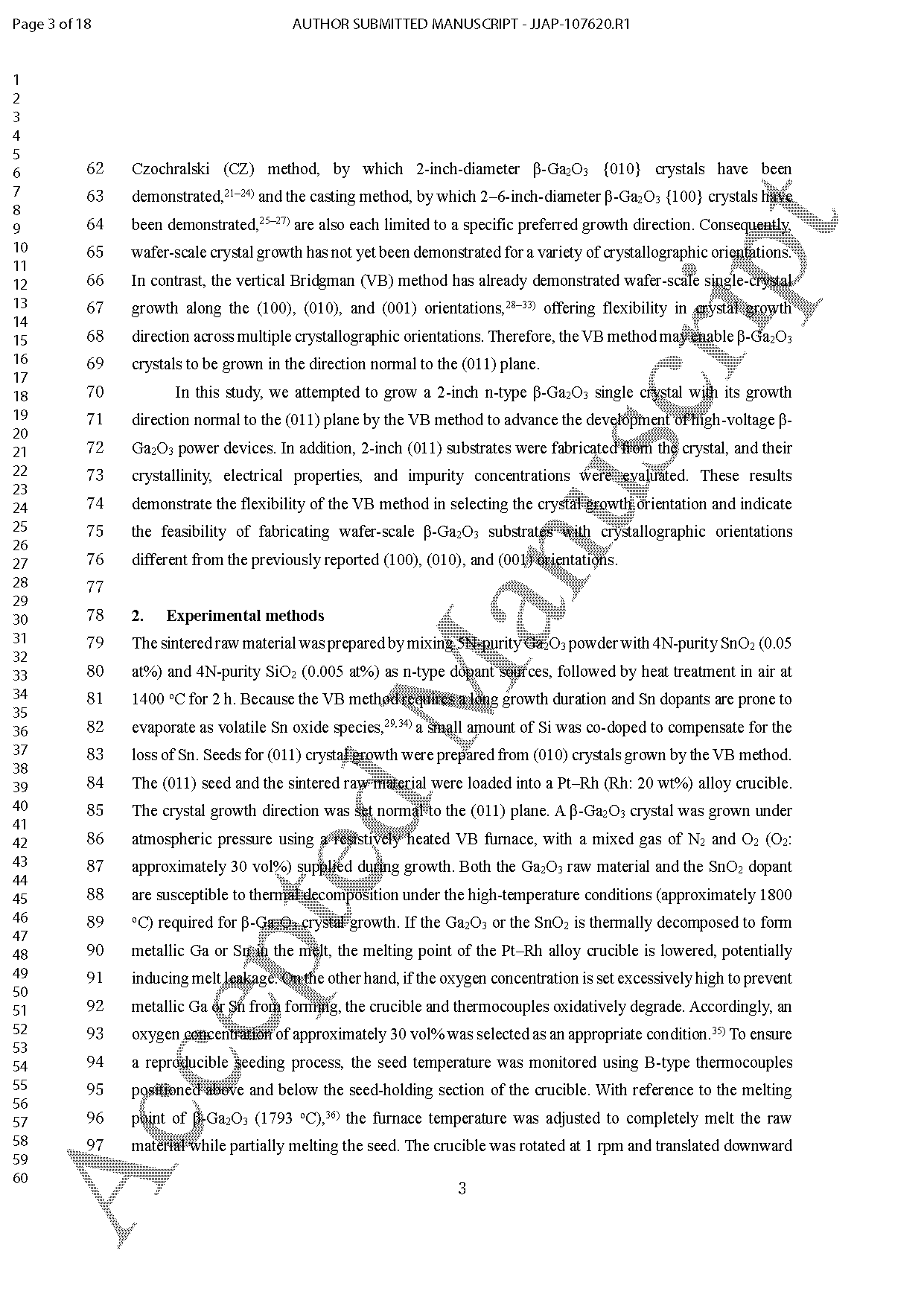
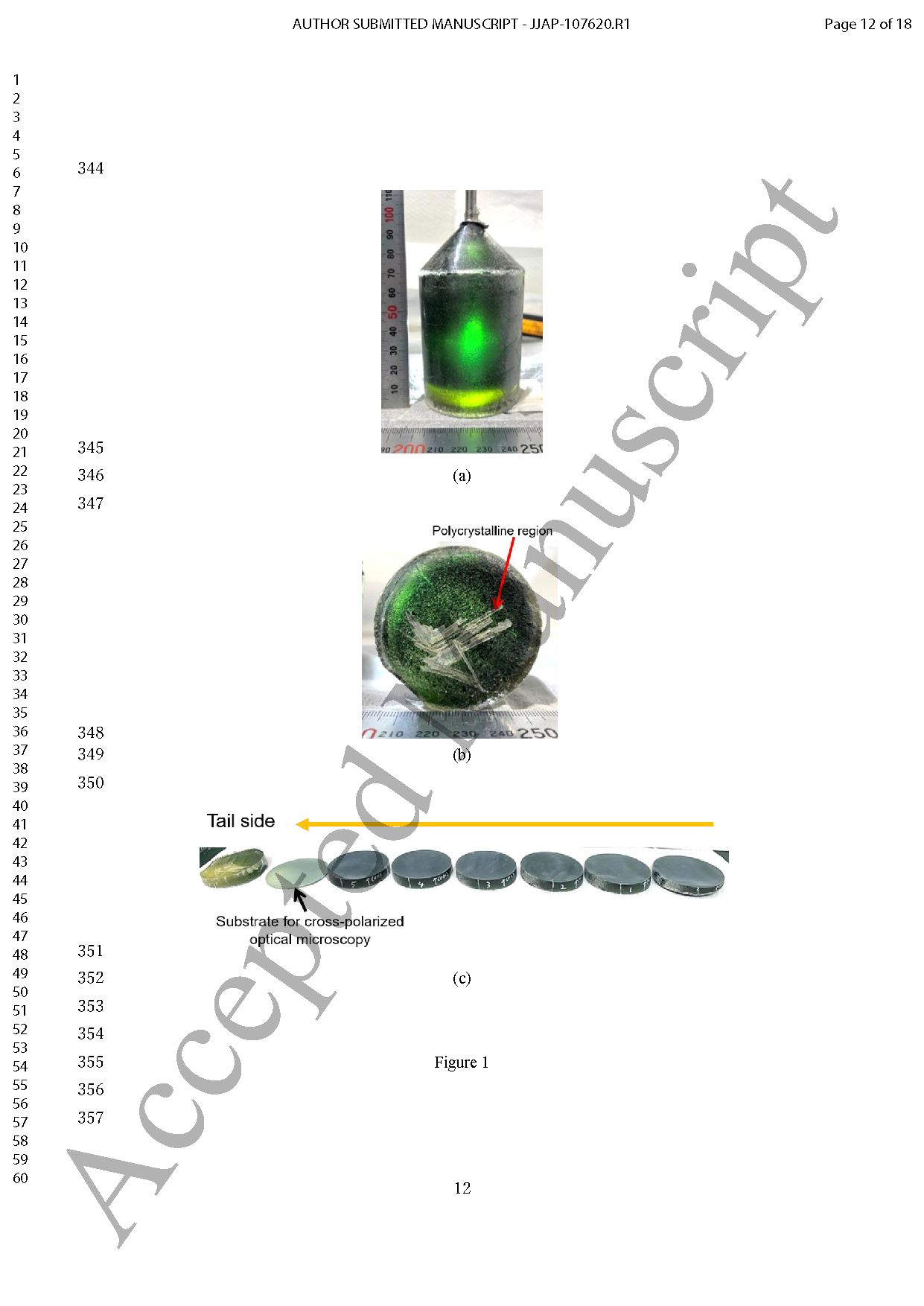
Figure 1. Photographs of (a) a 2-inch n-type β-Ga₂O₃ (011) crystal grown by the VB method, (b) the final solidification region, and (c) the sectioned crystal.
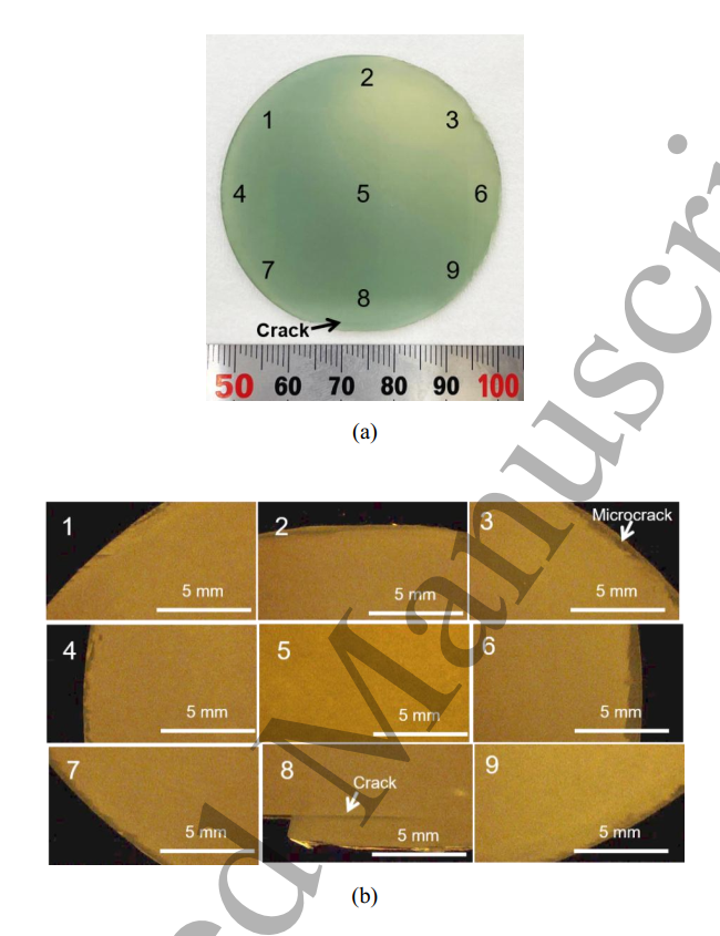
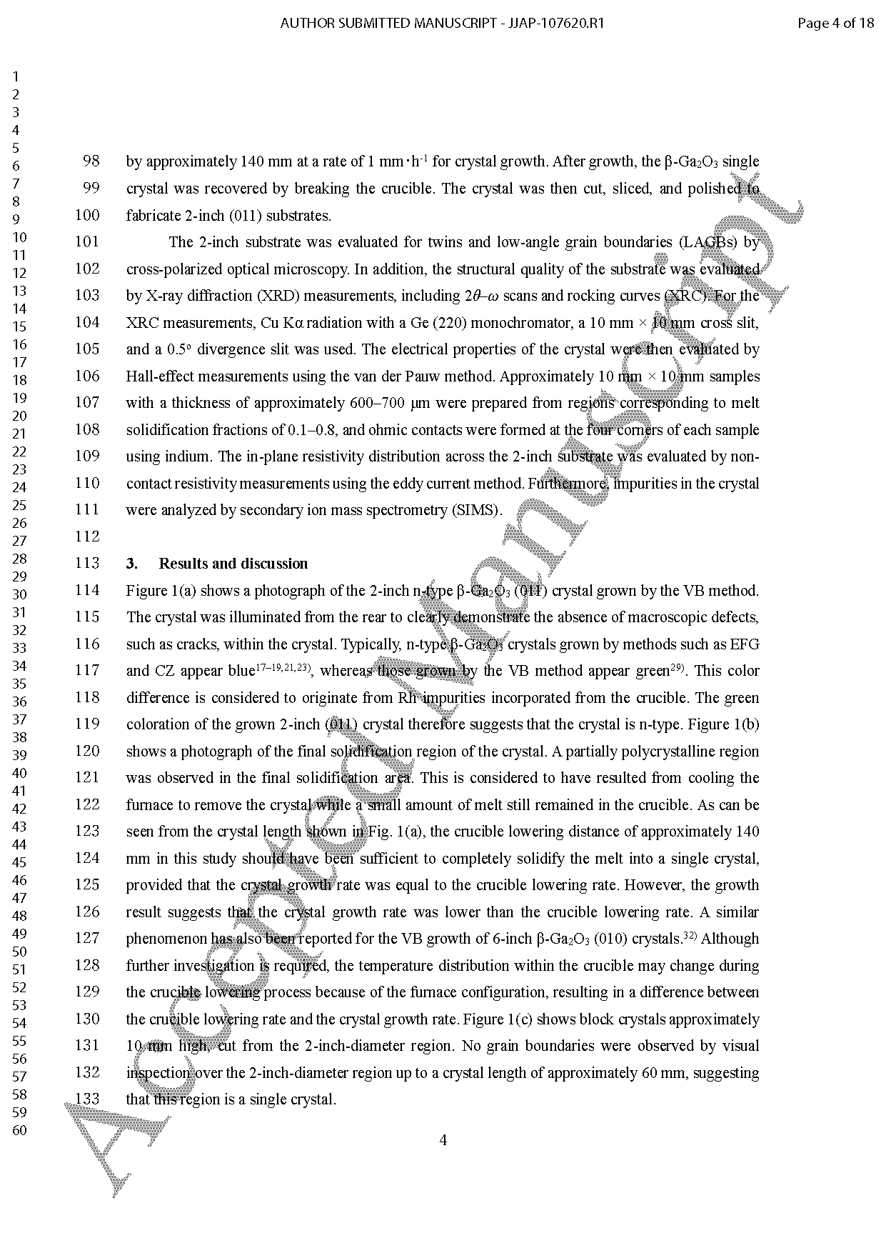
Figure 2. (a) 2-inch β-Ga₂O₃ (011) substrate obtained from near the crystal tail and (b) cross-polarized optical microscopy images acquired at the indicated locations.
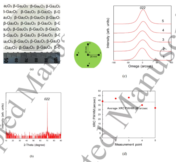
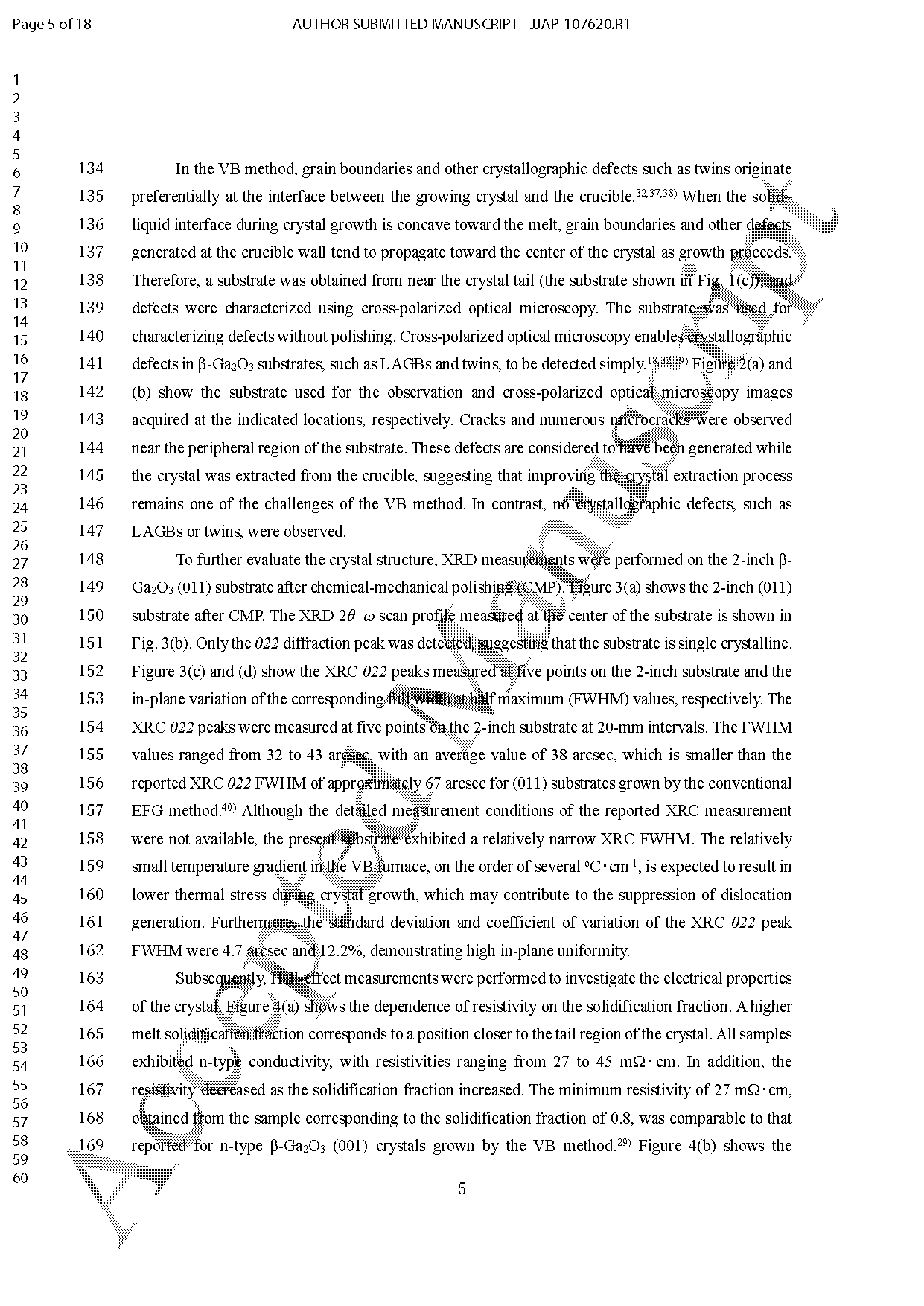
Figure 3. (a) 2-inch β-Ga₂O₃ (011) substrate after CMP, (b) XRD 2θ–ω scan profile measured near the wafer center, (c) XRC peaks of the 022 diffraction measured at five points on the 2-inch substrate, and (d) in-plane variation of the FWHM values.
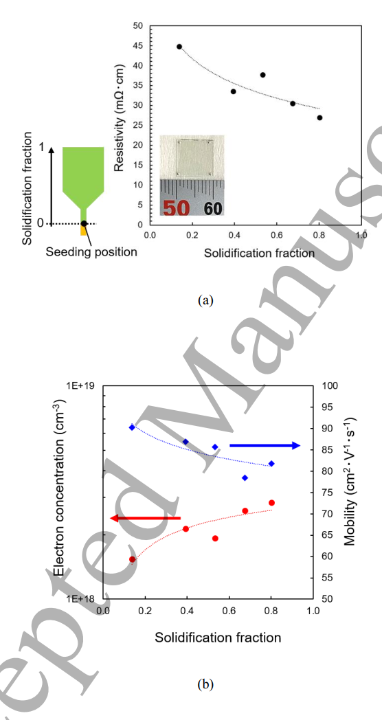
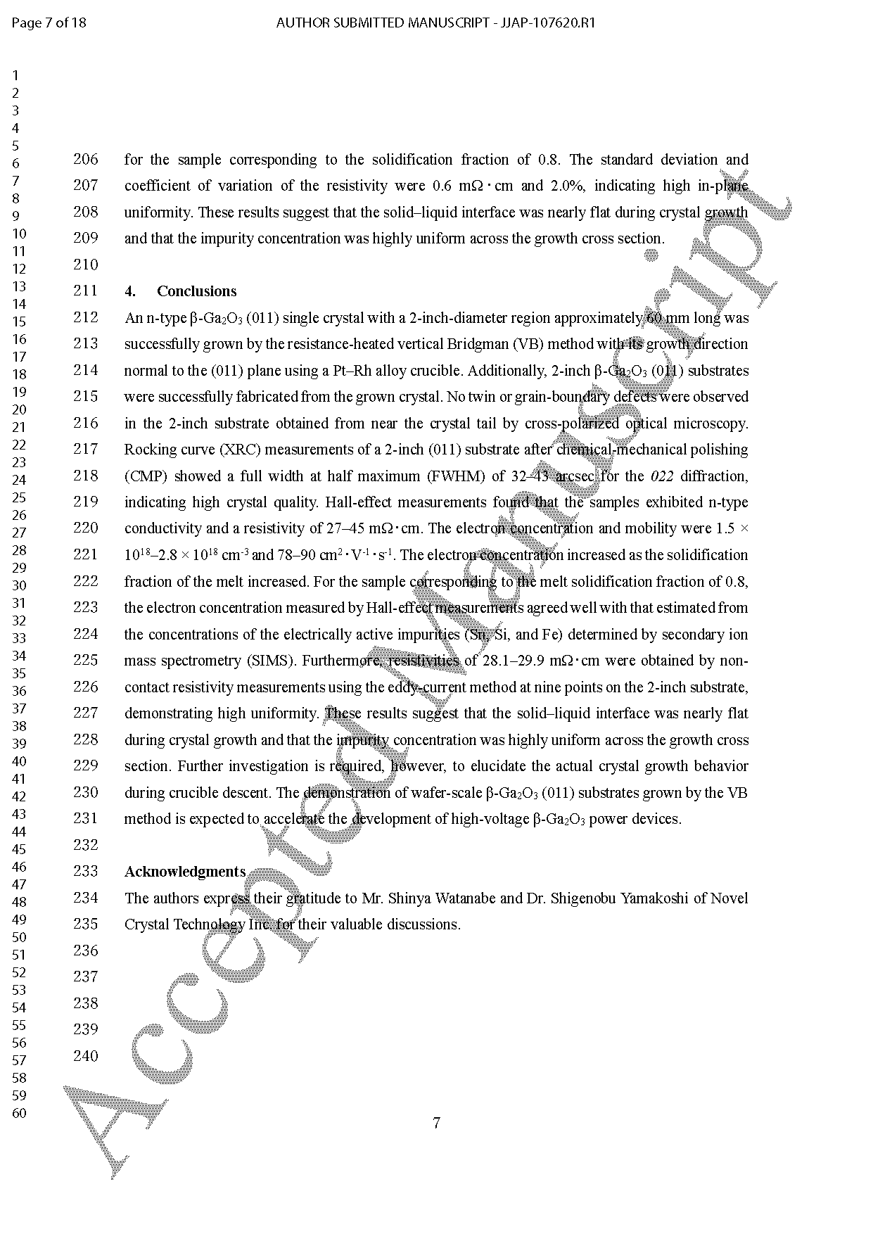
Figure 4. (a) Dependence of resistivity on the solidification fraction and (b) dependence of electron concentration and mobility on the solidification fraction.
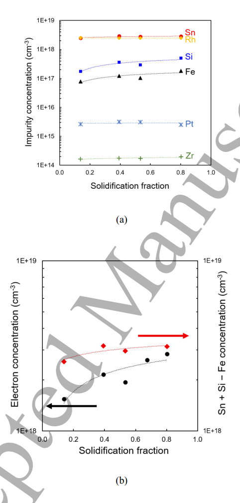
Figure 5. (a) Dependence of impurity concentration on the solidification fraction and (b) comparison of electron concentration with the calculated Sn + Si − Fe concentration.
DOI:
doi.org/10.35848/1347-4065/aeaf30


Instruction
Official Account

Cooperation
Top
