


Researchers from Xiamen University have published a research article titled "High-performance large-area β-Ga2O3 MIS trench Schottky barrier diodes with Al2O3/GaON interfacial insulators" in Applied Physics Letters. By in-situ forming an ultrathin GaON layer on the trench sidewalls via an atomic nitrogen beam treatment, and combining 60°-tilted fins with an Al2O3/GaON interfacial double layer, the team achieved a low specific on-resistance of 7.3 mΩ·cm2 with a high current/voltage capability of 10 A/670 V on a 1×2 mm2 large-area device, while reducing the interface trap density by one order of magnitude.
Background
β-Ga2O3 has emerged as a pivotal material for kilovolt-class power devices owing to its ultra-wide bandgap (~4.9 eV), high theoretical critical breakdown field (~8 MV/cm) and controllable n-type doping. Among β-Ga2O3 devices, vertical Schottky barrier diodes (SBDs) are highly competitive for high-power applications because of low conduction losses, high breakdown voltages and fast switching. However, conventional vertical SBDs suffer from localized breakdown caused by electric-field crowding at edges/corners and increased reverse leakage due to thermionic field emission at the Schottky contact. Trench MIS SBDs divert the peak field into the bulk semiconductor via a dielectric layer, yet local electric-field crowding still occurs at trench bottom corners, and sub-surface defects introduced during fin etching exacerbate dielectric leakage. For switch devices requiring both high current and high voltage, scaling up the active area inevitably introduces more defects. Therefore, suppressing dielectric leakage at trench sidewalls and reducing interface defect density in large-area devices remain critical challenges.
Abstract
In this work, the team fabricated a 1×2 mm2 large-area Ni/Al2O3/GaON/β-Ga2O3 MIS trench SBD on a HVPE-grown β-Ga₂O₃ epitaxial wafer (550 μm (001) substrate with 5×10¹⁸ cm-3 doping and a 10 μm drift layer with 2×10¹⁶ cm-3 doping. An atomic nitrogen beam (OXFORD HD25; 300 W, 4 sccm N₂, 10-2 Pa) was then irradiated onto the exposed trench sidewalls at room temperature for 2 h, in-situ forming an ultrathin GaON layer confirmed by HRTEM. The device with the GaON layer delivered a maximum forward current of ~10 A at V_F=9.5 V with Ron,sp of 7.3 mΩ·cm2 (comparable to 6.7 mΩ·cm2 for the reference), an ideality factor of 1.02, and a slightly increased turn-on voltage (0.72 to 0.75 V). Its breakdown voltage was 612–670 V, versus 365–407 V for the reference, with an I_on/I_off ratio above 10⁶ and a power figure of merit (VBR²/Ron,sp) of 61.5 MW/cm2, outperforming reported large-area (≥1×10⁻² cm2) β-Ga₂O₃ SBDs. Bias-stress measurements at -100 V for 1000 s confirmed stable operation. Temperature-dependent J-V-T analysis revealed that the reference device followed the Poole-Frenkel (PF) emission model, whereas the GaON-capped device showed weak temperature dependence and agreed well with the Fowler-Nordheim tunneling (FNT) model, indicating a leakage-mechanism transition from trap-assisted emission to tunneling. C-V measurements showed a positive flat-band shift from -0.2 to +5.6 V (Nox ≈ 2.9×1012 cm-2), and the interface trap density Dit was reduced from 2×10¹² to 1.5×10¹¹ eV-1·cm-2,about one order of magnitude lower.
Highlights
An in-situ trench-sidewall nitridation strategy using an atomic nitrogen beam: with the photoresist mask retained, only the trench inner walls are nitrided at room temperature to form an ultrathin GaON layer, without affecting the fin-top Schottky contact; the process is compatible with existing ICP etching and ALD.
An Al2O3/GaON double-layer interfacial insulator: inserted between Al₂O₃ and β-Ga2O3, the GaON layer broadens the depletion region, suppresses trap-related charging, and reduces Dit from 2×10¹² to 1.5×10¹¹ eV-1·cm-2 (one order of magnitude).
Co-optimized low conduction loss and high breakdown on a large area: a 1×2 mm2 device achieves Ron,sp of 7.3 mΩ·cm2, 10 A/670 V, an ideality factor of 1.02, and a PFOM of 61.5 MW/cm2, outperforming reported large-area β-Ga2O3 SBDs.
A reverse-leakage mechanism transition: the dominant leakage switches from temperature-sensitive Poole-Frenkel emission to weakly temperature-dependent Fowler-Nordheim tunneling, explaining the suppressed dielectric leakage and elevated breakdown voltage.
Conclusion
In summary, large-area (1×2 mm2) high-performance β-Ga₂O₃ trench SBDs featuring 60°-tilted fins and an ultrathin GaON interlayer have been demonstrated. The devices exhibit an ideality factor of 1.02, a low Ron,sp of 7.3 mΩ·cm2, and a high current/voltage of 10 A/670 V. The GaON interlayer optimizes the trench MIS interface by passivating oxygen vacancies, introducing favorable fixed charge, and modifying the dominant leakage mechanism-collectively reducing dielectric leakage under reverse bias and raising the breakdown voltage. These results demonstrate that the GaON layer is an effective approach for realizing next-generation β-Ga2O3 SBDs toward high-voltage power rectification.
Project Support
This work was supported by the Shenzhen Science and Technology Program (Grant No. JCJYJ20240813145617023) and the National Natural Science Foundation of China (Grant No. 62171396).
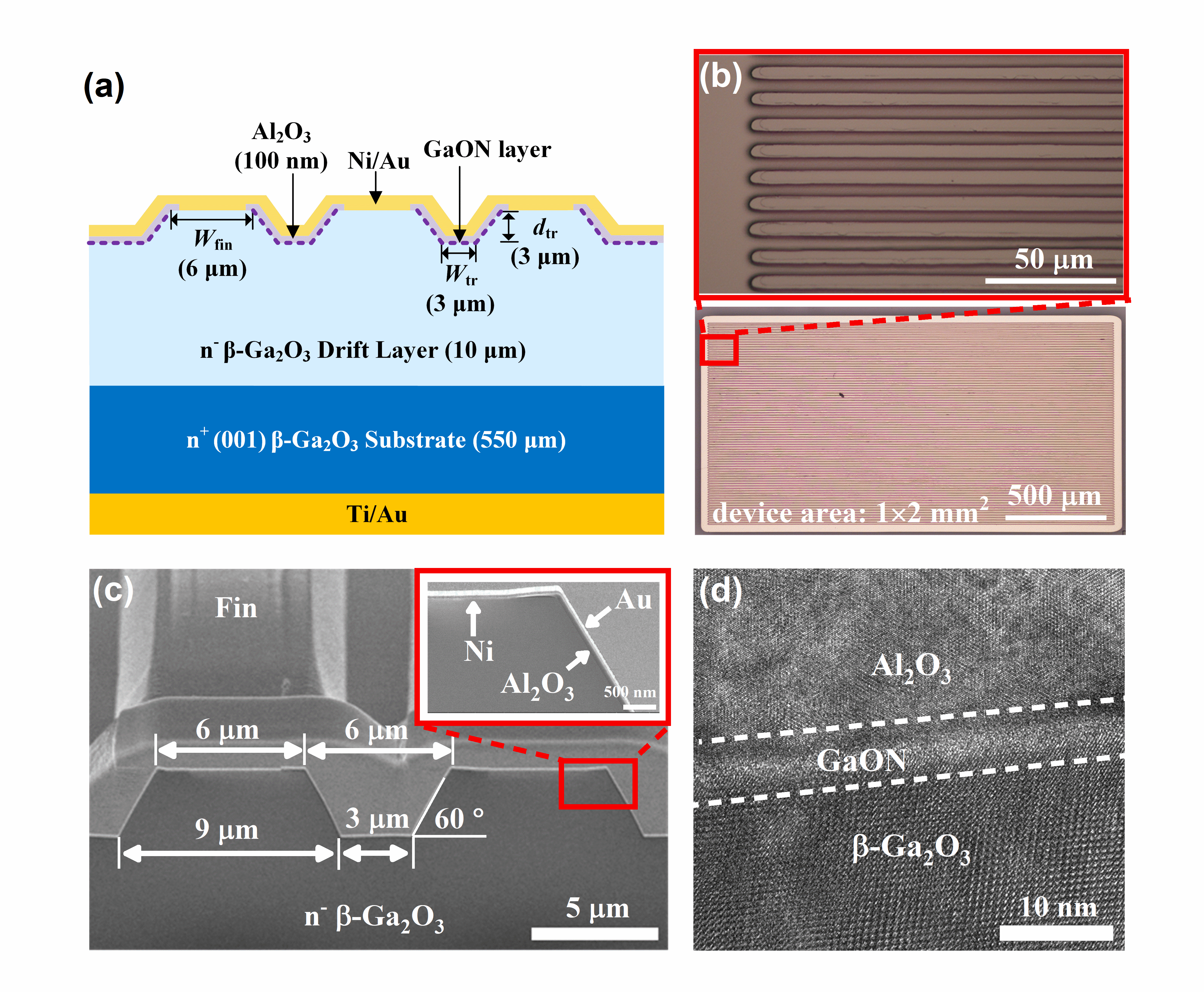
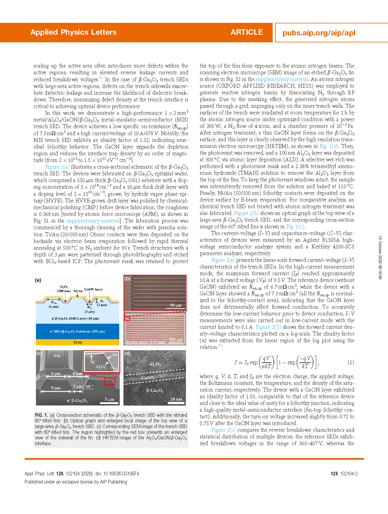
Figure 1. Cross-sectional schematic and morphology of the β-Ga₂O₃ trench SBD:(a) Cross-section schematic of the trench SBD with nitrided 60°-tilted fins. (b) Optical graph and enlarged SEM image of the top view of a large-area (1×2 mm²) device. (c) Cross-sectional SEM image of the trench Fin structure; the red-boxed region shows an enlarged view of the sidewall. (d) HRTEM image of the Al₂O₃/GaON/β-Ga₂O₃ interface.
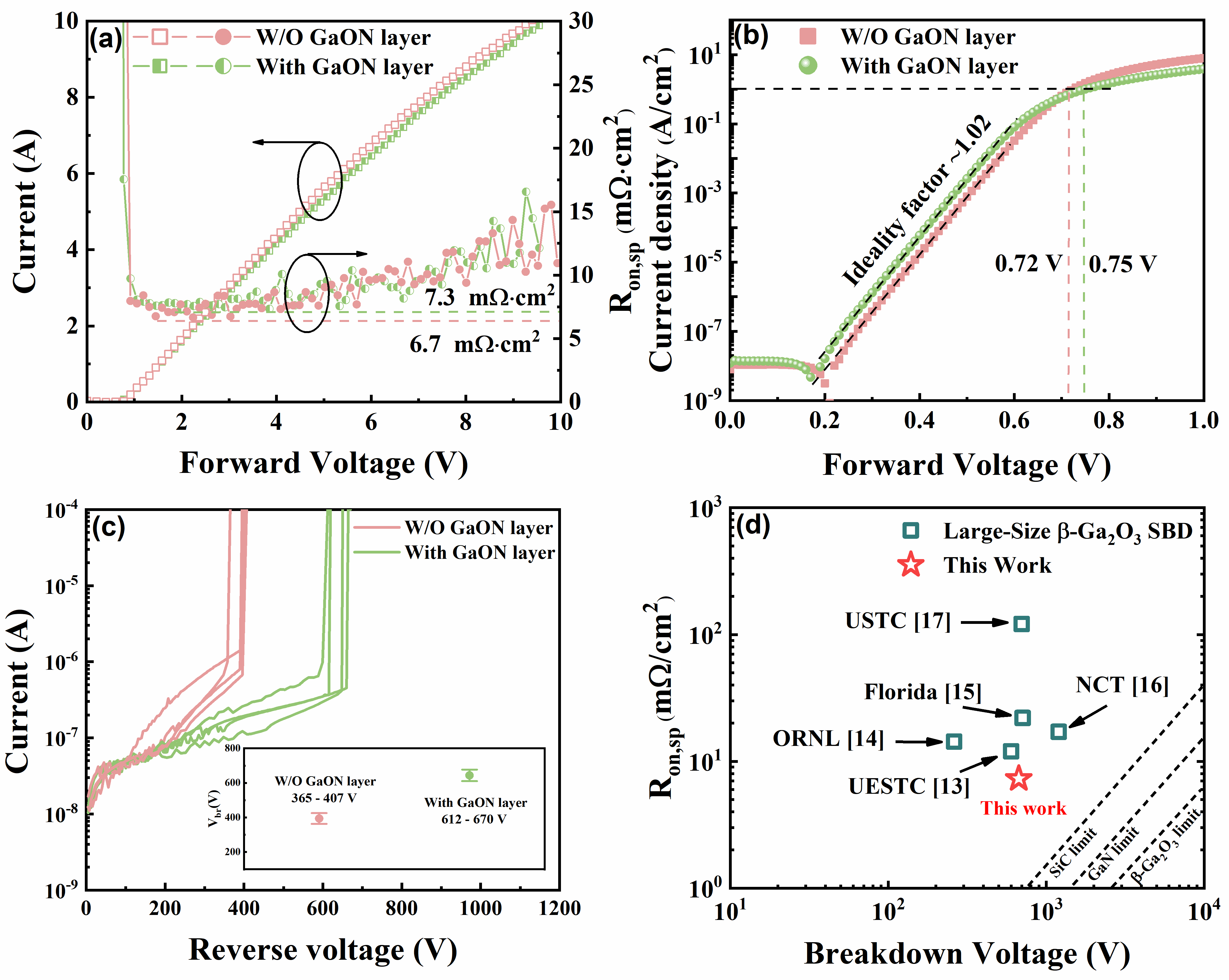
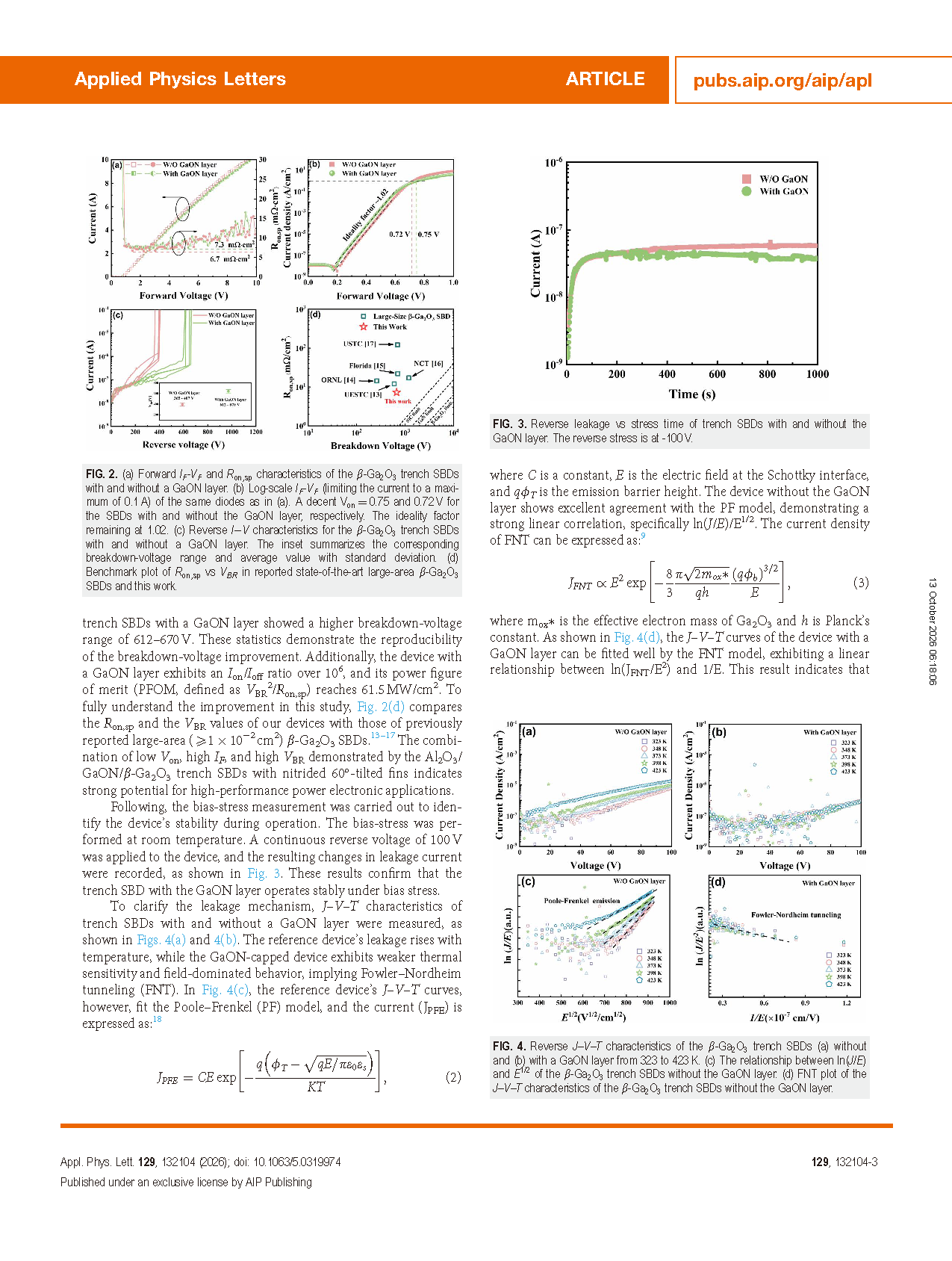
Figure 2. (a) Forward IF-VF and Ron,sp characteristics of the β-Ga2O3 trench SBDs with and without a GaON layer. (b) Log-scale IF-VF (limiting the current to a maximum of 0.1A) of the same diodes as in (a). A decent Von=0.75 and 0.72 V for the SBDs with and without the GaON layer, respectively. The ideality factor remaining at 1.02. (c) Reverse I-V characteristics for the β-Ga2O3 trench SBDs with and without a GaON layer. The inset summarizes the corresponding breakdown-voltage range and average value with standard deviation. (d) Benchmark plot of Ron,sp vs VBR in reported state-of-the-art large-area β-Ga2O3 SBDs and this work.
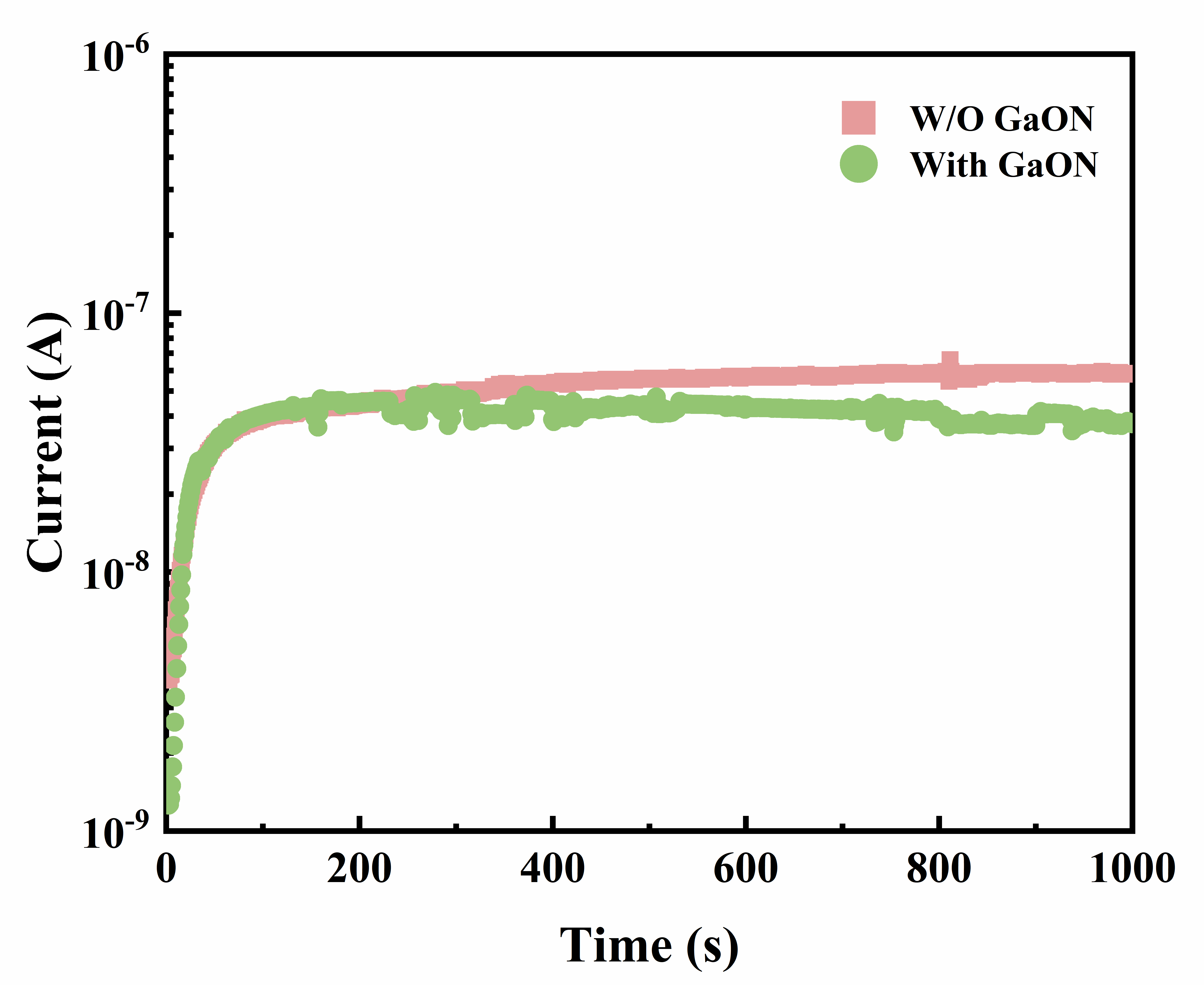
Figure 3. Reverse leakage vs stress time of trench SBDs with and without the GaON layer. The reverse stress is at -100V.
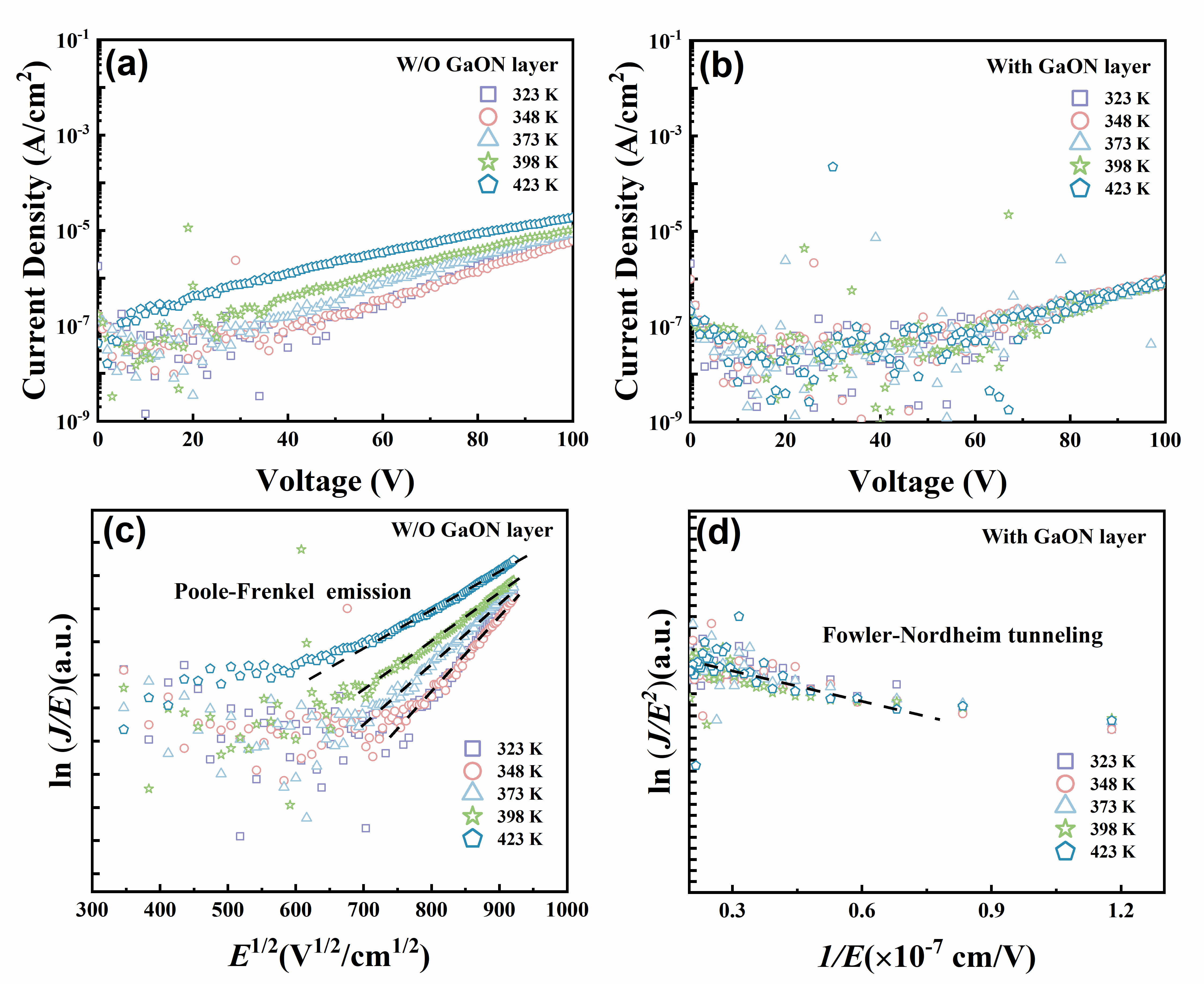
Figure 4. Reverse J-V-T characteristics (323-423 K) and leakage-mechanism fitting: J-V-T curves of devices (a) without and (b) with the GaON layer. (c) Poole-Frenkel (PF) plot of the reference device. (d) Fowler-Nordheim tunneling (FNT) plot of the GaON-capped device.
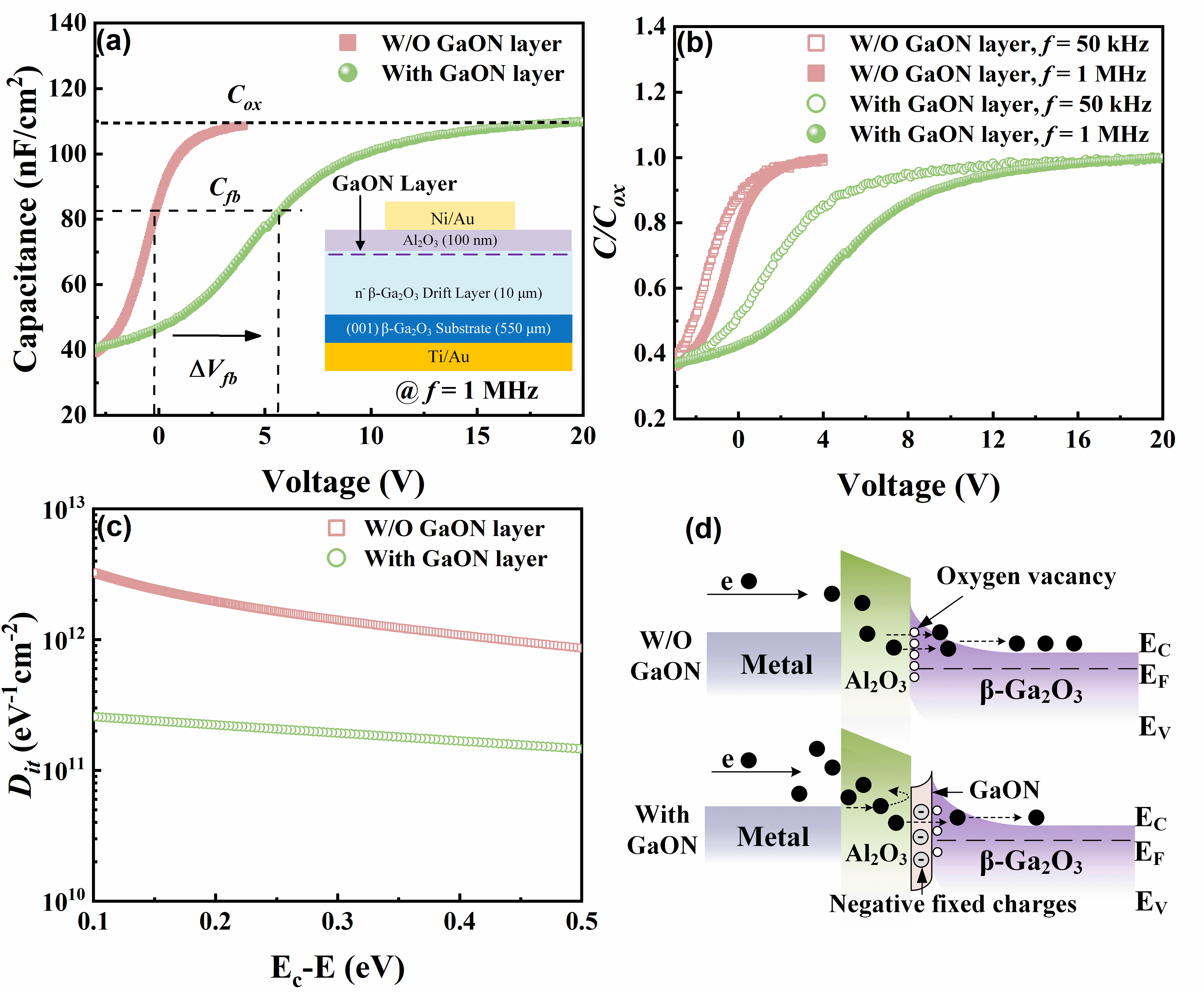
Figure 5. (a) C-V characteristics of the Al2O3/β-Ga2O3 MOSCAPs with and without a GaON layer, both measured at a frequency of 1MHz. (b) High-frequency and low-frequency C/Cox vs V of MOSCAPs with and without a GaON layer. (c) Dit distributions for Al2O3/β-Ga2O3 with and without a GaON layer when the conduction band minimum (Ec) of β-Ga2O3 ranges from 0.1 to 0.5 eV. (d) The electron transport process of MIS interfaces with and without a GaON layer at reverse bias. The black solid dots denote free electrons, and the white hollow dots denote oxygen vacancy.
Author Profiles

Zifan Hong, First Author. He received his PhD in Microelectronics and Solid-State Electronics from the School of Electronic Science and Engineering, Xiamen University. His research mainly focuses on Ga2O3 material growth and the design and fabrication of power devices.

Weifeng Yang, Corresponding Author. He is a Minjiang Scholar Distinguished Professor and PhD supervisor at Xiamen University. He was selected into the Fujian Provincial “Hundred Talents Program for Foreign Experts” and Xiamen “Double Hundred Program” for innovative talents. He previously conducted research at Nanyang Technological University, National University of Singapore, and A*STAR, Singapore. His long-term research interests include epitaxial growth and doping mechanisms of wide-bandgap and ultra-wide-bandgap semiconductors, device design and simulation, chip fabrication and module integration. He has published more than 100 academic papers in renowned international journals and conferences including Nature Physics, Energy Materials Storage, Advanced Science, Applied Physics Letters, IEEE Electron Device Letters, and IEEE Transactions on Electron Devices, and has filed/authorized over 20 invention patents.
DOI:
doi.org/10.1063/5.0319974
Instruction
Official Account

Cooperation
Top
