


Recently, GaFuture Semiconductor Technology (Jinjiang) Co., Ltd. (hereinafter referred to as "GaFuture Semiconductor") has made new progress in the development of α-gallium oxide (α-Ga₂O₃) epitaxial materials, successfully achieving wafer-scale epitaxial growth of 2-inch α-Ga₂O₃ on sapphire substrates. The company has made phased progress in key parameters, including crystal quality, epitaxial film thickness, and thickness uniformity.
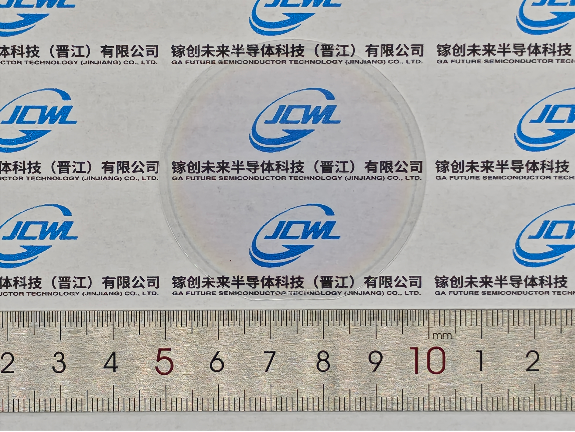
2-Inch Sapphire-Based α-Ga₂O₃ Heteroepitaxial Wafer
Gallium oxide is a next-generation ultra-wide-bandgap semiconductor material. Its metastable α phase (α-Ga₂O₃) offers distinct advantages. With a bandgap of approximately 5.3 eV, α-Ga₂O₃ shares the corundum crystal structure with sapphire, providing good crystallographic compatibility and a favorable foundation for high-quality heteroepitaxial growth. Meanwhile, continued advances in isomorphic alloy systems and p-type materials are creating more possibilities for power device structure design.
Crystal quality, film thickness, and thickness uniformity are key parameters for epitaxial materials intended for device development. Achieving consistent performance across wafer-scale growth requires precise control of the growth process. GaFuture Semiconductor combines customized equipment with in-house process development, carrying out coordinated optimization of the temperature field, flow field, and chamber conditions while continuously refining its growth processes. This latest progress reflects the company's accumulated expertise in epitaxial growth and film thickness control, providing a foundation for further improvements in product performance.
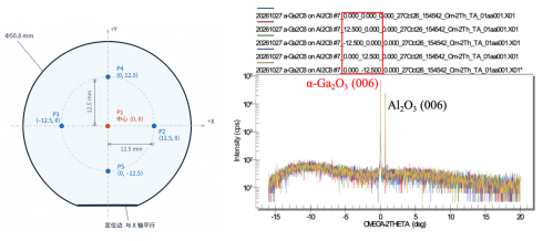
Five-Point Wafer Measurement Locations and X-Ray Diffraction Results
According to a third-party test report, GaFuture Semiconductor's 2-inch sapphire-based α-Ga₂O₃ heteroepitaxial wafer exhibits no detectable secondary phases. The epitaxial film thickness is approximately 3 μm, with thickness non-uniformity of less than 3%. Five-point measurements of the X-ray rocking curve (XRC) for the symmetric α-Ga₂O₃ (0006) reflection yielded a minimum full width at half maximum (FWHM) of 26.85 arcsec and an average of approximately 35.26 arcsec. The FWHM of the rocking curve for the asymmetric (10-14) reflection was 1,483.95 arcsec. These results indicate that GaFuture Semiconductor's α-Ga₂O₃ heteroepitaxial products have reached an internationally advanced level.
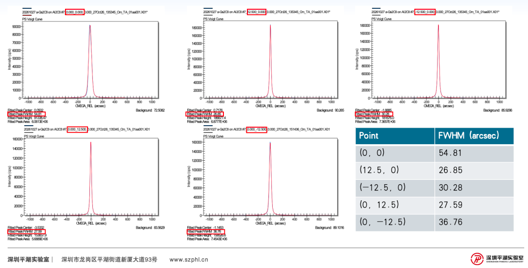
Five-Point X-Ray Rocking Curves and FWHM of the (0006) Reflection for the Epitaxial Wafer
Furthermore, to address the thermal management requirements of gallium oxide power devices, GaFuture Semiconductor has collaborated with universities, including Xidian University and Xi'an University of Technology, to investigate the growth of β-Ga₂O₃ thin films on silicon carbide (SiC), aluminum nitride (AlN), and diamond substrates. Given the intrinsically low thermal conductivity of gallium oxide, the research explores thin-film growth conditions and material properties on highly thermally conductive substrates, providing a reference for subsequent studies of heat transfer at the film–substrate interface.
Preliminary characterization results show that, for a 20 mm × 20 mm SiC-based β-Ga₂O₃ epitaxial sample, the full width at half maximum (FWHM) of the ω-scan rocking curve can be as low as 400 arcsec. For a 2-inch wafer-scale sample, the X-ray diffraction (XRD) pattern exhibits the (−201), (−402), and (−603) diffraction peaks, with an ω-scan rocking curve FWHM of approximately 0.95°. Under the investigated process conditions, β-Ga₂O₃ thin films grown on AlN substrates achieved a minimum ω-scan rocking curve FWHM of 1.60° and a minimum surface roughness of 1.72 nm. For films grown on diamond substrates, the minimum ω-scan rocking curve FWHM was 1.64°.
These preliminary advances in the growth and characterization of gallium oxide epitaxial films on highly thermally conductive substrates provide a foundation for further optimization of growth processes, investigation of material properties, and exploration of potential device applications.
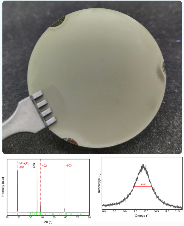
2-Inch SiC-Based β-Ga₂O₃ Epitaxial Wafer and Its X-Ray Diffraction Characterization Results: The upper image shows a photograph of the sample; the lower-left image shows the X-ray diffraction pattern; and the lower-right image shows the ω-scan rocking curve
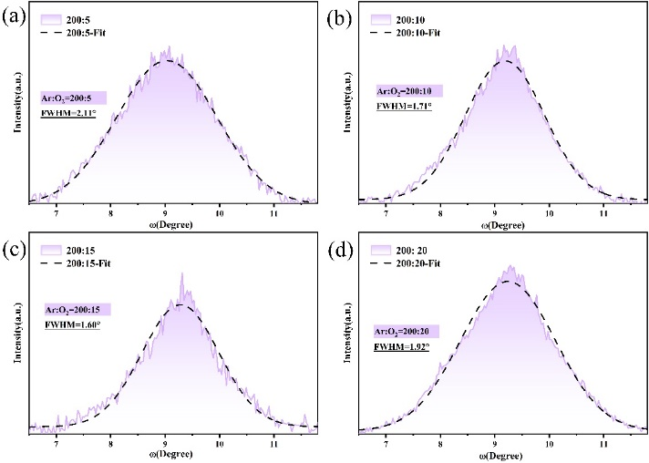
ω-Scan Rocking Curves of β-Ga₂O₃ Epitaxial Films on AlN Substrates under Different Argon-to-Oxygen Ratios
GaFuture Semiconductor continues to advance the performance optimization of gallium oxide heteroepitaxial materials, building process expertise in crystal quality and film thickness control to support the continued iteration and upgrading of its products.
About GaFuture Semiconductor
GaFuture Semiconductor Technology (Jinjiang) Co., Ltd. specializes in the development of gallium oxide semiconductor materials and epitaxial products. Leveraging highly customized equipment and an in-house process development platform, the company provides gallium oxide epitaxial material services tailored to the needs of research institutions, device development teams, and industry customers, supporting the development and application of gallium oxide materials.
For more information about GaFuture Semiconductor's gallium oxide epitaxial products or to discuss potential collaborations, please feel free to contact the company.
Product Inquiries and Business Cooperation
Contact: Mr. Lu
Tel: +86 19503417793 (also available on WeChat)
Email: gaofuture2025@163.com
Instruction
Official Account

Cooperation
Top