


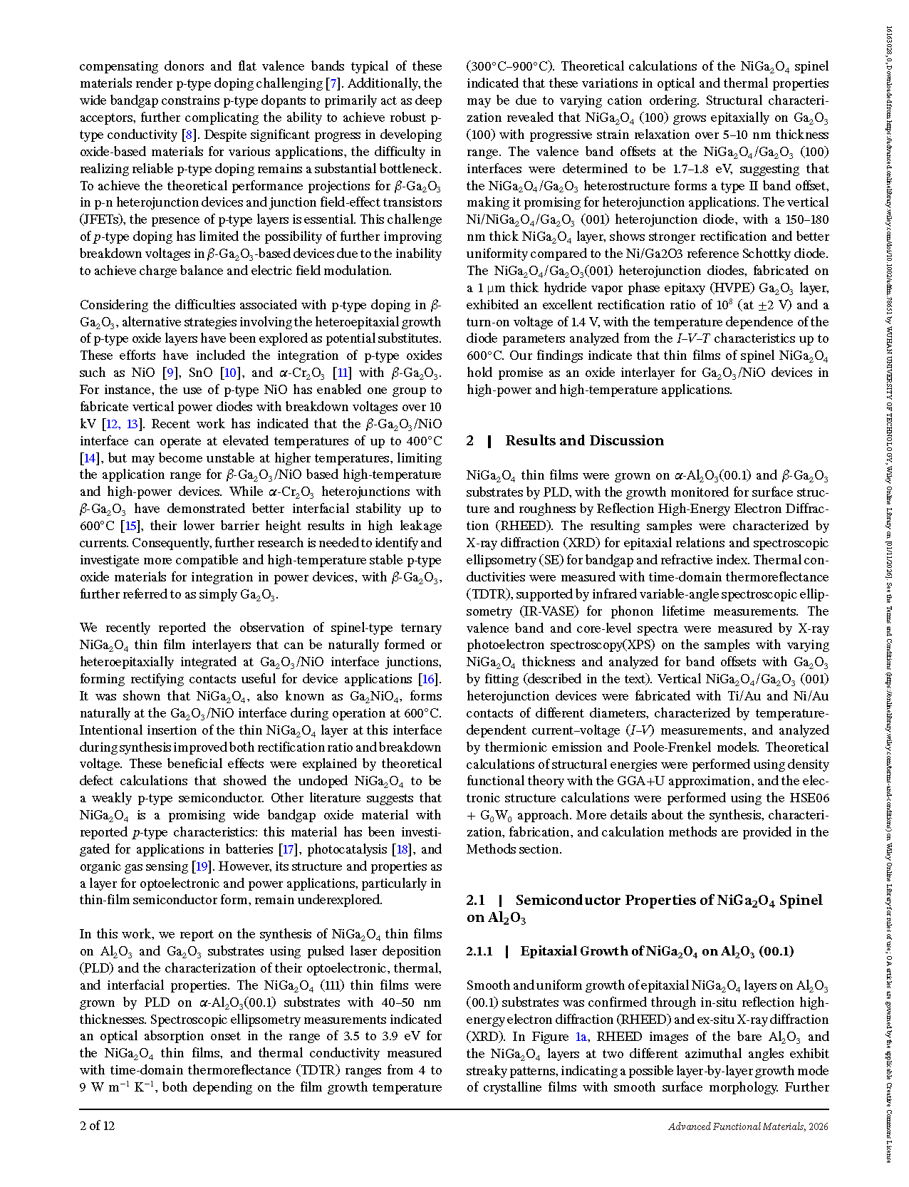
Researchers from the National Laboratory of the Rockies, Colorado School of Mines and University of Virginia have published a paper titled "Epitaxial Growth and Semiconductor Properties of NiGa₂O₄ Spinel and its Interfaces with Ga₂O₃" in Advanced Functional Materials.
Background
Monoclinic gallium oxide (β-Ga₂O₃) is an emerging ultra-wide-bandgap semiconducting oxide, recognized for its promise in electronic and photonic applications. β-Ga₂O₃ is predicted to sustain a critical electric field strength of 8 MV/cm, potentially surpassing the performance of current commercial materials such as SiC and GaN in high-voltage devices and power electronics. With a bandgap of 4.8 eV, β-Ga₂O₃ is also suited for solar-blind detection, sensing, and transparent conductor applications within the deep ultraviolet (UV) spectrum. However, progress in power electronic devices utilizing oxide-based UWBG materials like β-Ga₂O₃ has been constrained by the challenge of ambipolar doping. NiO-based heterojunctions suffer from limited thermal stability above 400 ℃, while α-Cr₂O₃ exhibits high leakage current despite improved temperature tolerance. It has been reported that spinel NiGa₂O₄ interlayer can naturally form at Ga₂O₃/NiO interfaces and improve device performance. Nevertheless, the epitaxial growth, optoelectronic-thermal properties, band offsets and high-temperature device behaviors of NiGa₂O₄ thin films remain poorly understood. In this work, pulsed laser deposition is adopted to fabricate NiGa₂O₄ epitaxial films. Structural, optical and thermal properties are systematically characterized. Valence band offset at NiGa₂O₄/Ga₂O₃ interface is measured, and heterojunction diodes are fabricated to verify its potential for high-temperature power devices.
Abstract
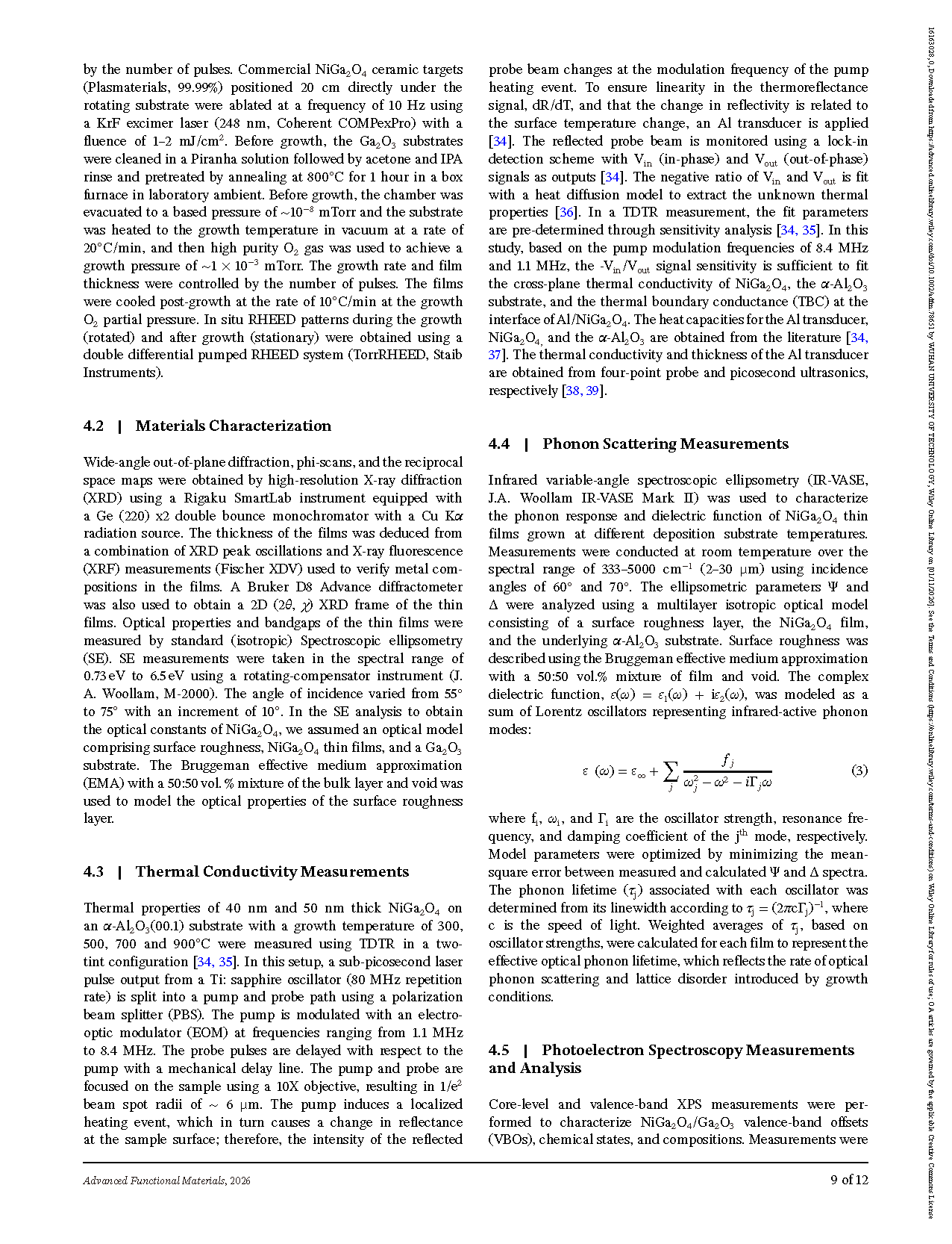
Unintentionally formed interfacial layers are ubiquitous in semiconductor devices that operate at extreme conditions, but their structure and properties remain unknown due to the layer thinness. Here, we present epitaxial growth and semiconductor properties of NiGa₂O₄ spinel and its interfaces with Ga₂O₃ in high-power and high-temperature electronic devices. Cubic spinel NiGa₂O₄ films of 2–200 nm thicknesses and low surface roughness ( ∼ 2 nm) were grown on (0001) α-Al₂O₃ using pulsed laser deposition at substrate temperatures in the 300–900◦C range. The NiGa₂O₄ optical absorption onset (3.6–3.9 eV) and thermal conductivity (4-9 W m⁻¹ K⁻¹) vary systematically with substrate temperature, consistent with theoretical predictions of varying Ni and Ga cation ordering on the spinel lattice. The valence band offset at the epitaxial NiGa₂O₄/Ga₂O₃ interfaces of (100) orientation is determined to be 1.8 eV using a new method that addresses limitations of traditional Kraut analysis. The NiGa₂O₄/Ga₂O₃ heterojunction devices with (001) HVPE drift layers exhibit a rectification ratio of 10⁸ (for ± 2V) and a turn-on voltage of 1.4 V, maintaining diode behavior up to 600◦C. These results highlight the potential of NiGa₂O₄ as a heterojunction partner in β-Ga₂O₃-based devices and show a new approach to investigate such interfacial layers.
Highlights
Epitaxial spinel NiGa₂O₄ thin films are realized on α-Al₂O₃(0001). Optical and thermal properties are demonstrated to be governed by cation ordering within spinel lattice.
NiGa₂O₄ grows epitaxially on Ga₂O₃(100). Coherent strain is preserved below critical thickness of 5-10 nm, and strain relaxation occurs for thicker films.
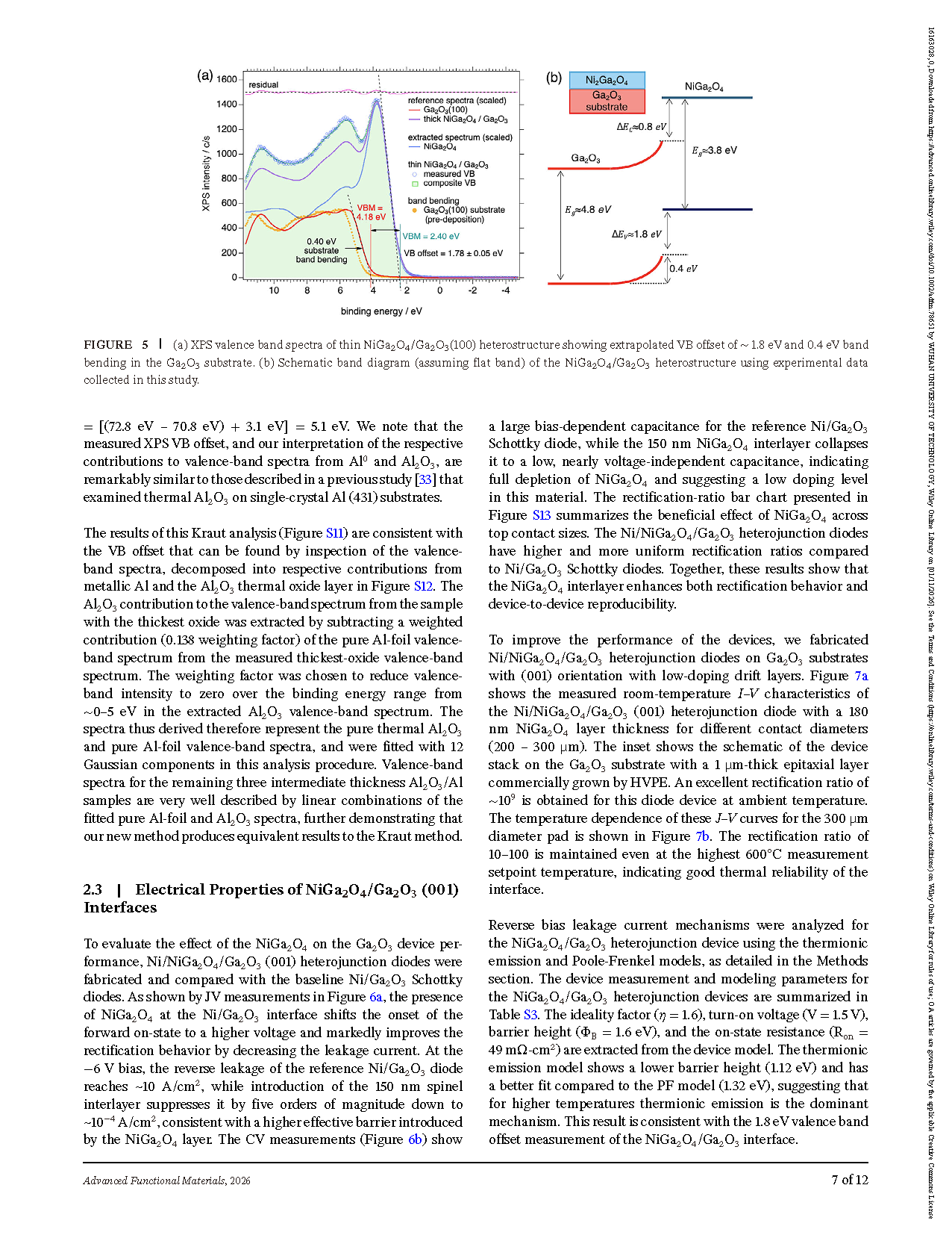
A novel XPS valence-band fitting method is developed to overcome limitations of conventional Kraut approach. Valence band offset of NiGa₂O₄/Ga₂O₃(100) is measured as 1.8 eV, validated by Al₂O₃/Al reference system.
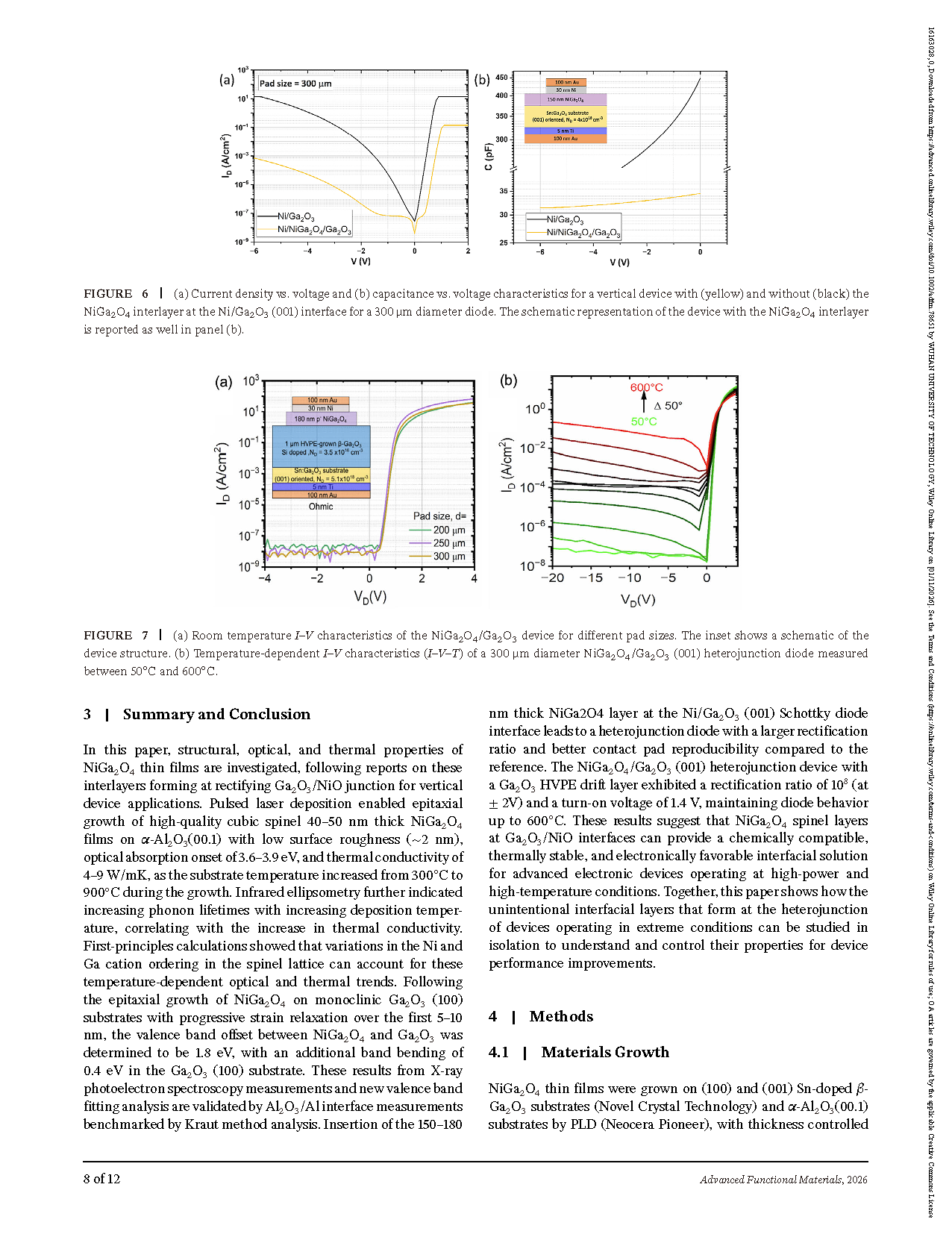
Vertical Ni/NiGa₂O₄/Ga₂O₃ heterojunction diodes are fabricated. Compared with Ni/Ga₂O₃ Schottky reference diodes, reverse leakage is greatly suppressed and device uniformity is improved.
The heterojunction diode delivers rectification ratio of 10⁸ at ± 2 V and turn-on voltage of 1.4 V, retaining diode performance up to 600 ℃. NiGa₂O₄ is verified as promising interfacial candidate for high-temperature high-power Ga₂O₃ devices.
Conclusion
In this paper, structural, optical, and thermal properties of NiGa₂O₄ thin films are investigated, following reports on these interlayers forming at rectifying Ga₂O₃/NiO junction for vertical device applications. Pulsed laser deposition enabled epitaxial growth of high-quality cubic spinel 40–50 nm thick NiGa₂O₄ films on α-Al₂O₃ (00.1) with low surface roughness ( ∼ 2 nm), optical absorption onset of 3.6–3.8 eV, and thermal conductivity of 4–9 W/mK, as the substrate temperature increased from 300◦C to 900◦C during the growth. Infrared ellipsometry further indicated increasing phonon lifetimes with increasing deposition temperature, correlating with the increase in thermal conductivity. First‑principles calculations showed that variations in the Ni and Ga cation ordering in the spinel lattice can account for these temperature‑dependent optical and thermal trends. Following the epitaxial growth of NiGa₂O₄ on monoclinic Ga₂O₃ (100) substrates with progressive strain relaxation over the first 5–10 nm, the valence band offset between NiGa₂O₄ and Ga₂O₃ was determined to be 1.8 eV, with an additional band bending of 0.4 eV in the Ga₂O₃ (100) substrate. These results from X‑ray photoelectron spectroscopy measurements and new valence‑band fitting analysis are validated by Al₂O₃/Al interface measurements benchmarked by Kraut method analysis. Insertion of the 150–180 nm thick NiGa₂O₄ layer at the Ni/Ga₂O₃ (001) Schottky diode interface leads to a heterojunction diode with a larger rectification ratio and better contact‑pad reproducibility compared to the reference. The NiGa₂O₄/Ga₂O₃ (001) heterojunction device with a Ga₂O₃ HVPE drift layer exhibited a rectification ratio of 10⁸ (at ± 2V) and a turn‑on voltage of 1.4 V, maintaining diode behavior up to 600◦C. These results suggest that NiGa₂O₄ spinel layers at Ga₂O₃/NiO interfaces can provide a chemically compatible, thermally stable, and electronically favorable interfacial solution for advanced electronic devices operating at high‑power and high‑temperature conditions. Together, this paper shows how the unintentional interfacial layers that form at the heterojunction of devices operating in extreme conditions can be studied in isolation to understand and control their properties for device performance improvements.
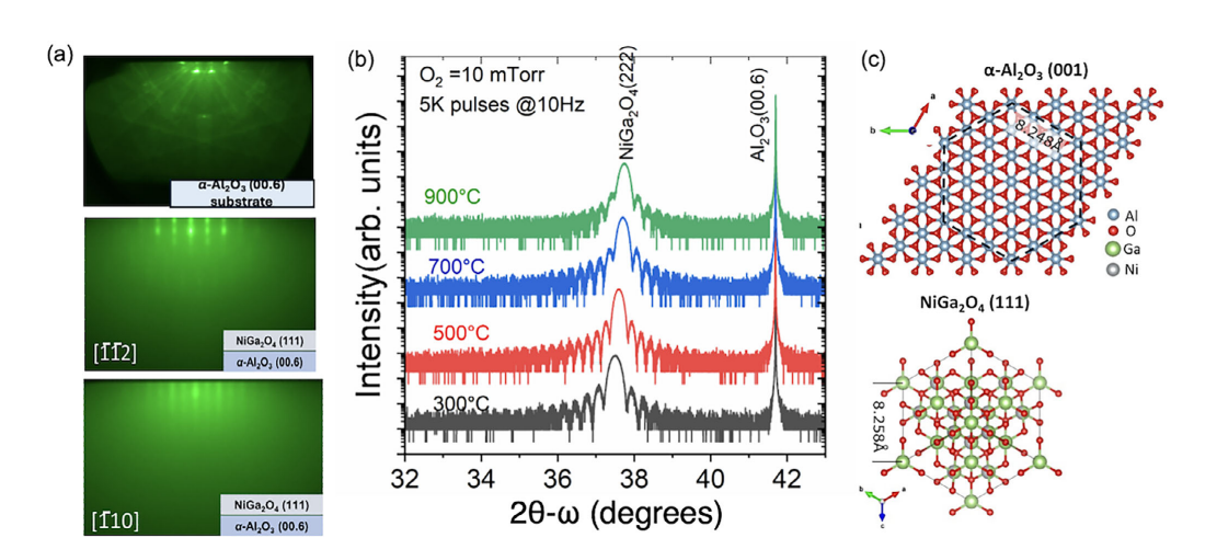
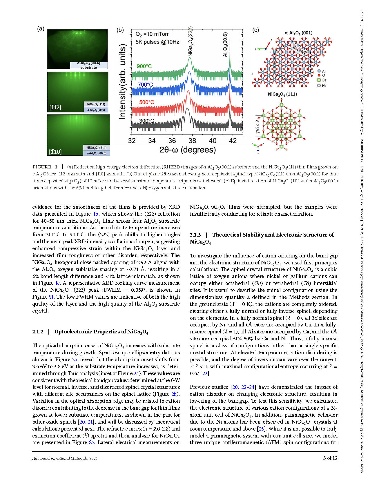
Figure 1. (a) Reflection high‑energy electron diffraction (RHEED) images of α-Al₂O₃ (00.1) substrate and the NiGa₂O₄(111) thin films grown on c-Al₂O₃ for [112]-azimuth and [110]-azimuth. (b) Out‑of‑plane 2 θ‑ ω scan showing heteroepitaxial spinel‑type NiGa₂O₄(111) on α-Al₂O₃(00.1) for thin films deposited at p(O₂) of 10 mTorr and several substrate temperature setpoints as indicated. (c) Epitaxial relation of NiGa₂O₄(111) and α-Al₂O₃(00.1) orientations with the 6 % bond length difference and < 1 % oxygen sublattice mismatch.
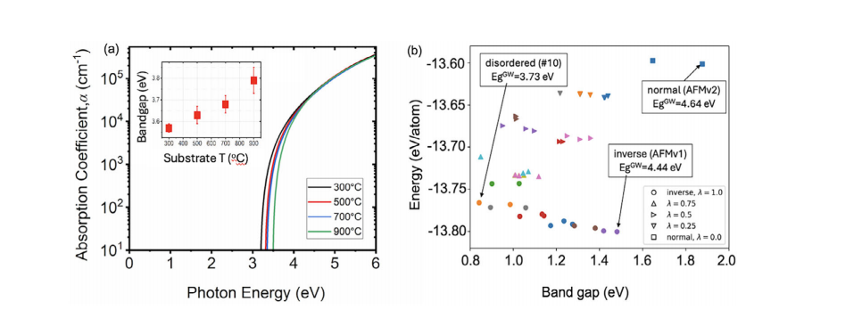
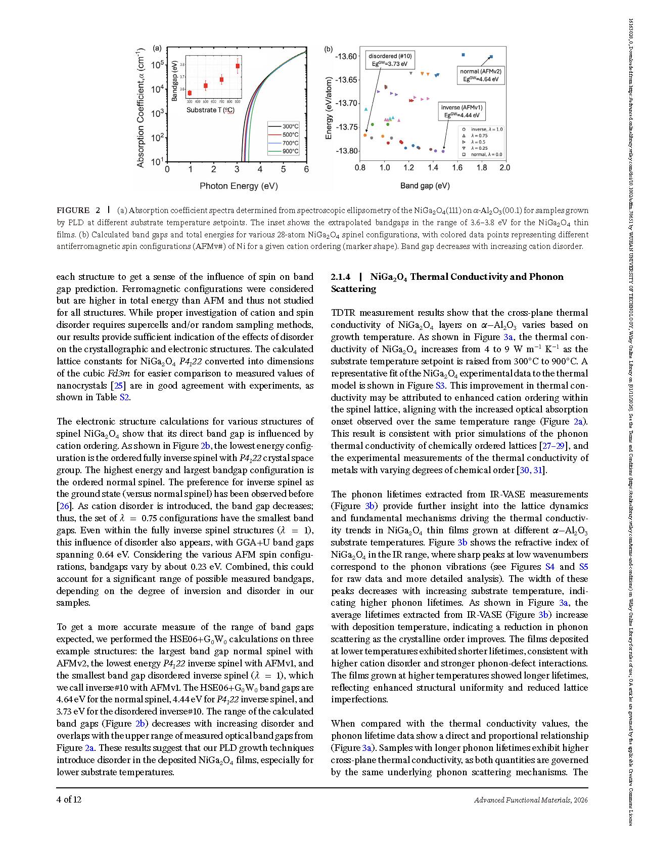
Figure 2. (a) Absorption coefficient spectra determined from spectroscopic ellipsometry of the NiGa₂O₄(111) on α-Al₂O₃ (00.1) for samples grown by PLD at different substrate temperature setpoints. The inset shows the extrapolated bandgaps in the range of 3.6–3.8 eV for the NiGa₂O₄ thin films. (b) Calculated band gaps and total energies for various 28‑atom NiGa₂O₄ spinel configurations, with colored data points representing different antiferromagnetic spin configurations (AFMv#) of Ni for a given cation ordering (marker shape). Band gap decreases with increasing cation disorder.
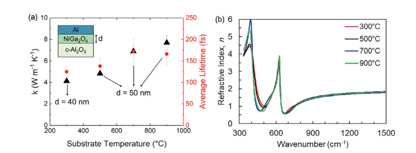
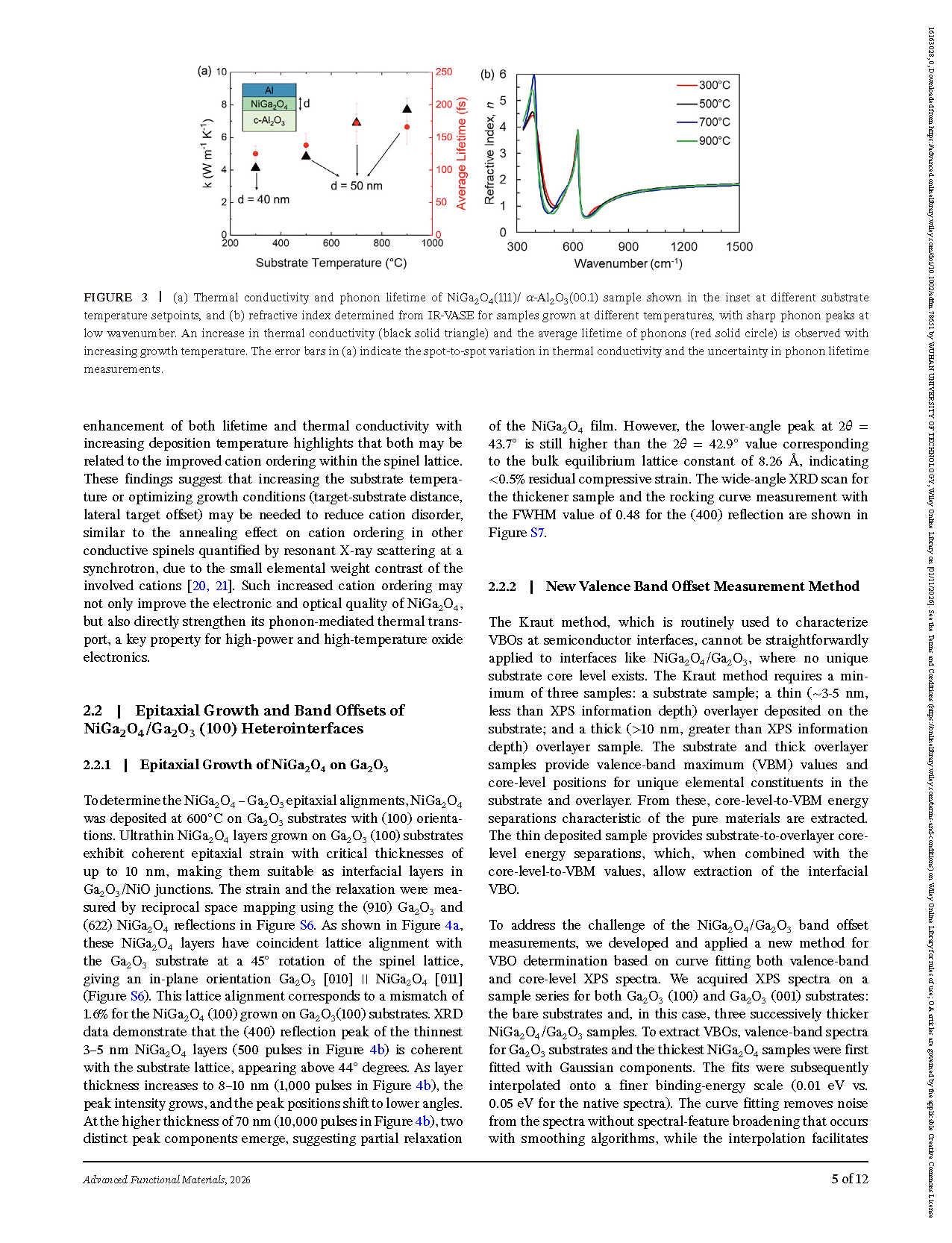
Figure 3. (a) Thermal conductivity and phonon lifetime of NiGa₂O₄(111)/α-Al₂O₃(00.1) sample shown in the inset at different substrate temperature setpoints, and (b) refractive index determined from IR-VASE for samples grown at different temperatures, with sharp phonon peaks at low wavenumber. An increase in thermal conductivity (black solid triangle) and the average lifetime of phonons (red solid circle) is observed with increasing growth temperature. The error bars in (a) indicate the spot‑to‑spot variation in thermal conductivity and the uncertainty in phonon lifetime measurements.
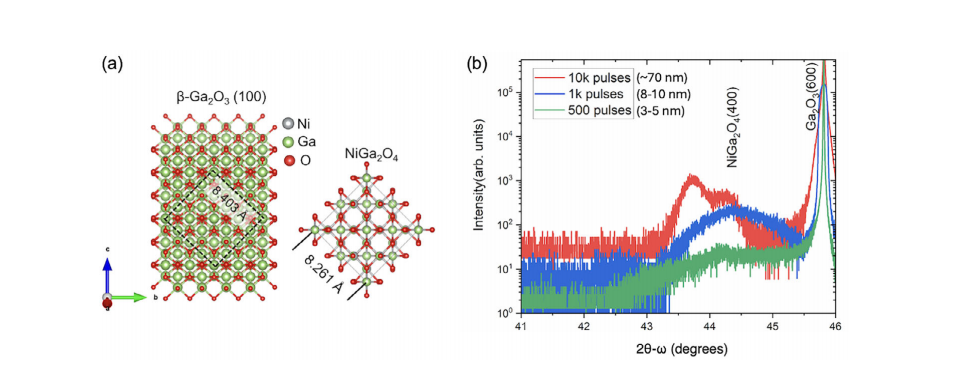
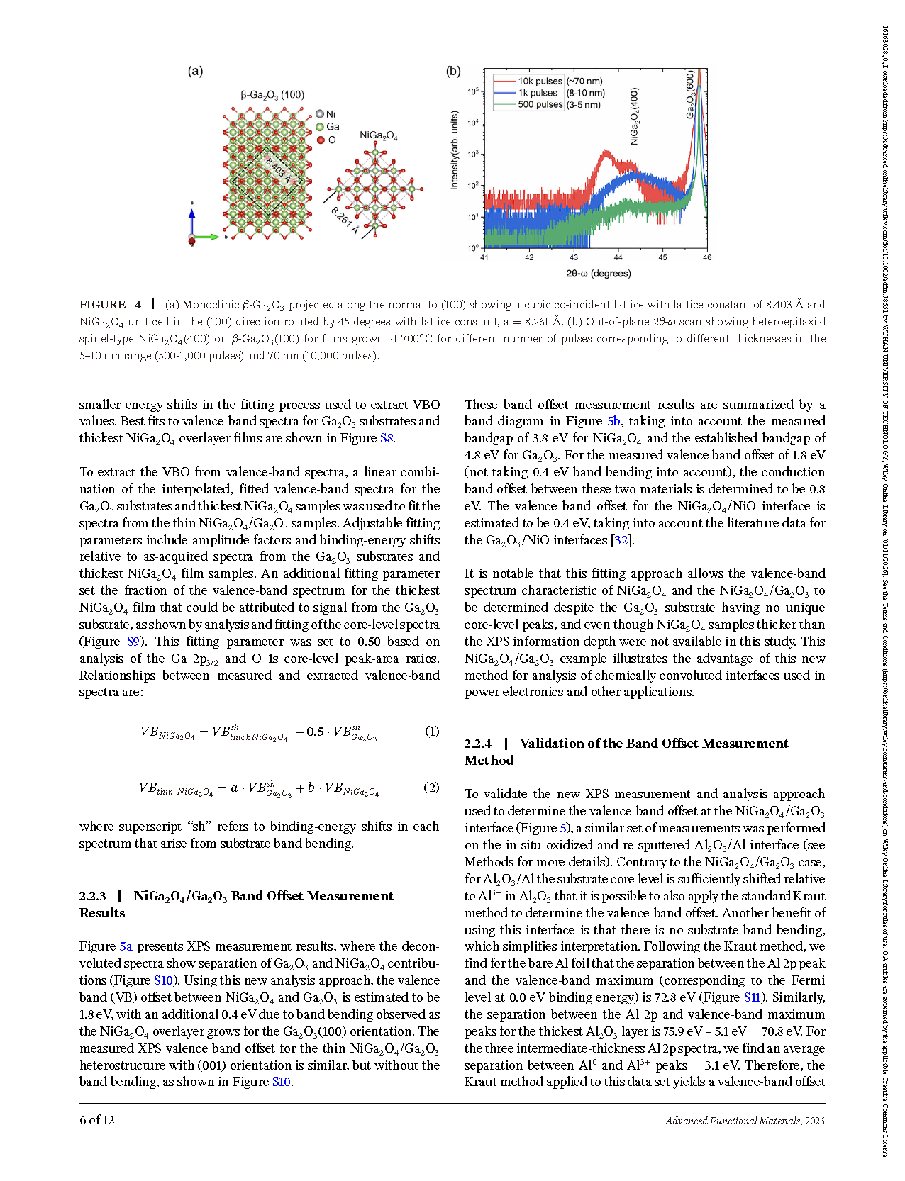
Figure 4. (a) Monoclinic β-Ga₂O₃ projected along the normal to (100) showing a cubic co‑incident lattice with lattice constant of 8.403 Å and NiGa₂O₄ unit cell in the (100) direction rotated by 45 degrees with lattice constant, a=8.261 Å. (b) Out‑of‑plane 2 θ‑ ω scan showing heteroepitaxial spinel‑type NiGa₂O₄(400) on β-Ga₂O₃(100) for films grown at 700◦C for different number of pulses corresponding to different thicknesses in the 5–10 nm range (500-1,000 pulses) and 70 nm (10,000 pulses).
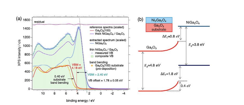
Figure 5. (a) XPS valence band spectra of thin NiGa₂O₄/Ga₂O₃(100) heterostructure showing extrapolated VB offset of ∼ 1.8 eV and 0.4 eV band bending in the Ga₂O₃ substrate. (b) Schematic band diagram (assuming flat band) of the NiGa₂O₄/Ga₂O₃ heterostructure using experimental data collected in this study.
DOI:
10.1002/adfm.78651
Instruction
Official Account

Cooperation
Top