


Researchers from The University of Tokyo have published a dissertation titled "Impact of oxidation conditions in SiO₂ atomic layer deposition on interface state densities at β-Ga₂O₃ (001) MOS interfaces with 600 °C post-deposition annealing" in Applied Physics Letters.
Background
β-Ga₂O₃ is regarded as a promising next-generation power semiconductor due to its wide bandgap (4.4–4.7 eV) and high breakdown electric field. Furthermore, the feasibility of growing bulk crystals from molten Ga₂O₃ via the edge-defined film-fed growth (EFG) method enables the fabrication of large-diameter wafers, paving the way for cost-effective manufacturing. Although successful demonstrations have been reported for high-voltage Schottky barrier diodes, the realization of high-performance β-Ga₂O₃ metal–oxide–semiconductor field-effect transistors (MOSFETs) remains a major challenge for several reasons. Since p-type doping techniques for β-Ga₂O₃ have not yet been established, it is inherently difficult to adopt conventional transistor architectures. Therefore, enhancement-mode operation has predominantly been demonstrated with fin-shaped channel structures, even though planar transistor formation remains a viable alternative if an electron channel can be formed on a nitrogen-doped semi-insulating layer.
Abstract
We investigated the impact of SiO2 film deposition conditions in either thermal or plasma-enhanced atomic layer depositions (ALDs) on the interface characteristics of β-Ga2O3 metal–oxide–semiconductor (MOS) capacitors, especially focusing on oxidation reaction conditions in ALD. The formation of the interface with an interface state density as low as ∼1011 eV−1 cm−2 at 0.2 eV below the conduction band edge and a low near-interface oxide trap density was achieved by tuning the O3-dose in thermal-ALD, with a post-deposition-annealing temperature limited to a relatively low temperature of 600 °C to avoid the thermally induced damages on Ga2O3. The fixed charge density at the SiO2/β-Ga2O3 interface was also minimized by thermal-ALD with the sufficient dose of O3. These results demonstrate the significant role of the control of SiO2 deposition conditions to achieve high-quality SiO2/β-Ga2O3 MOS interfaces with low-thermal-budget processes.
Highlights
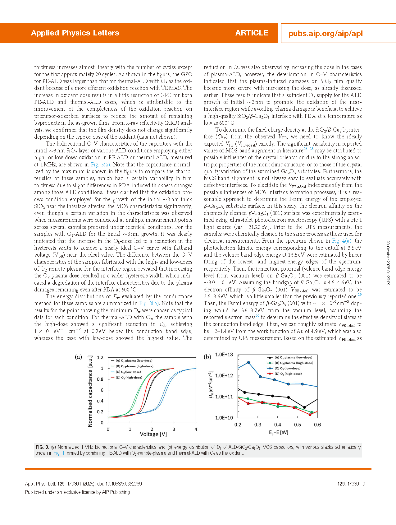
The study found that, compared with PE-ALD using remote O₂plasma, thermal ALD using O₃is more effective at reducing the interface state density and the density of traps in the near-interface oxide layer, whilst avoiding the impact of plasma damage on the electrical properties of the interface.
It was found that there is an optimal O₃supply dose for both the interfacial state density and the trap density in the near-interface oxide layer, indicating that excessive oxidation does not necessarily improve interfacial quality, and that oxidation conditions require precise control.
A methodology for the preparation of SiO₂/β-Ga₂O₃(001) interfaces suitable for low-thermal-budget processes has been established, demonstrating that by optimising the ALD oxidation reaction conditions, low levels of interfacial defects and fixed chargecan still be achieved even when the post-deposition annealing temperature is limited to 600 °C.
Conclusion
In conclusion, we investigated the impact of SiO2 deposition conditions via ALD on the SiO2/β-Ga2O3 (001) MOS characteristics, focusing especially on the oxidant supply during the ALD growth of the initial ~3 nm on β-Ga2O3. The use of O3 as an oxidant in thermal-ALD was found to be more efficient than the employment of O2-remote-plasma-ALD in reducing both Dit and Qtrap after PDA at a relatively low temperature (600°C), which is required to avoid thermally induced damages on the Ga2O3 properties. Our results indicate that controlling the oxidation reactions in the SiO2 film deposition processes has a significant influence on the formation of high-quality MOS interfaces of SiO2/β-Ga2O3 with PDA of limited thermal budget.
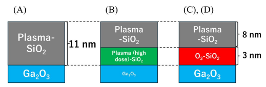
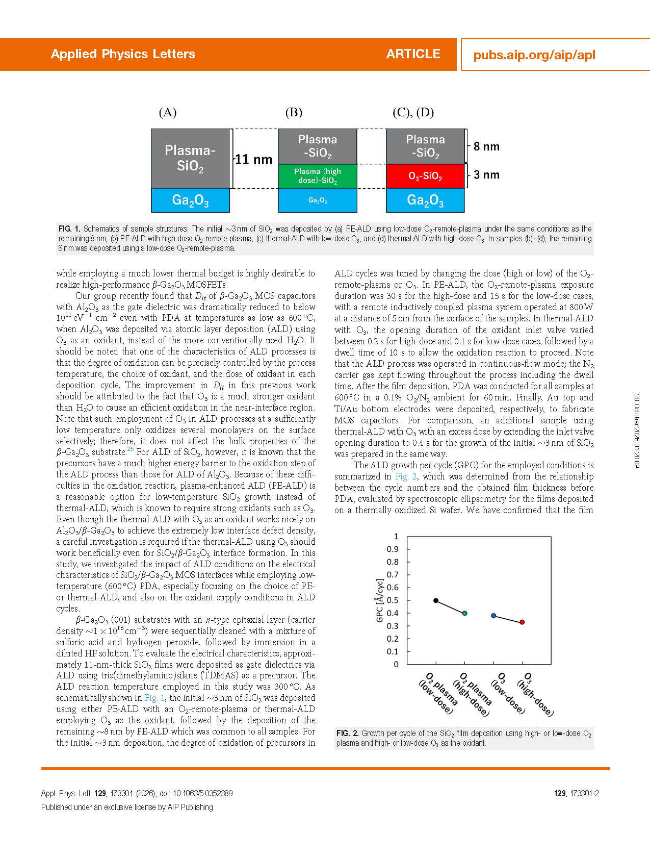
FIG. 1. Schematics of sample structures. The initial ~3 nm of SiO2 was deposited by (a) PE-ALD using low-dose O2-remote-plasma under the same conditions as the remaining 8 nm, (b) PE-ALD with high-dose O2-remote-plasma, (c) thermal-ALD with low-dose O3, and (d) thermal-ALD with high-dose O3. In samples (b)–(d), the remaining 8 nm was deposited using a low-dose O2-remote-plasma.
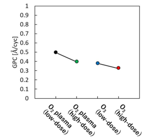
FIG. 2. Growth per cycle of the SiO2 film deposition using high- or low-dose O2 plasma and high- or low-dose O3 as the oxidant.
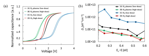
FIG. 3. (a) Normalized 1MHz bidirectional C–V characteristics and (b) energy distribution of Dit of ALD-SiO2/Ga2O3 MOS capacitors, with various stacks schematically shown in Fig. 1 formed by combining PE-ALD with O2-remote-plasma and thermal-ALD with O3 as the oxidant.
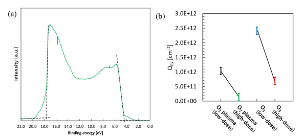
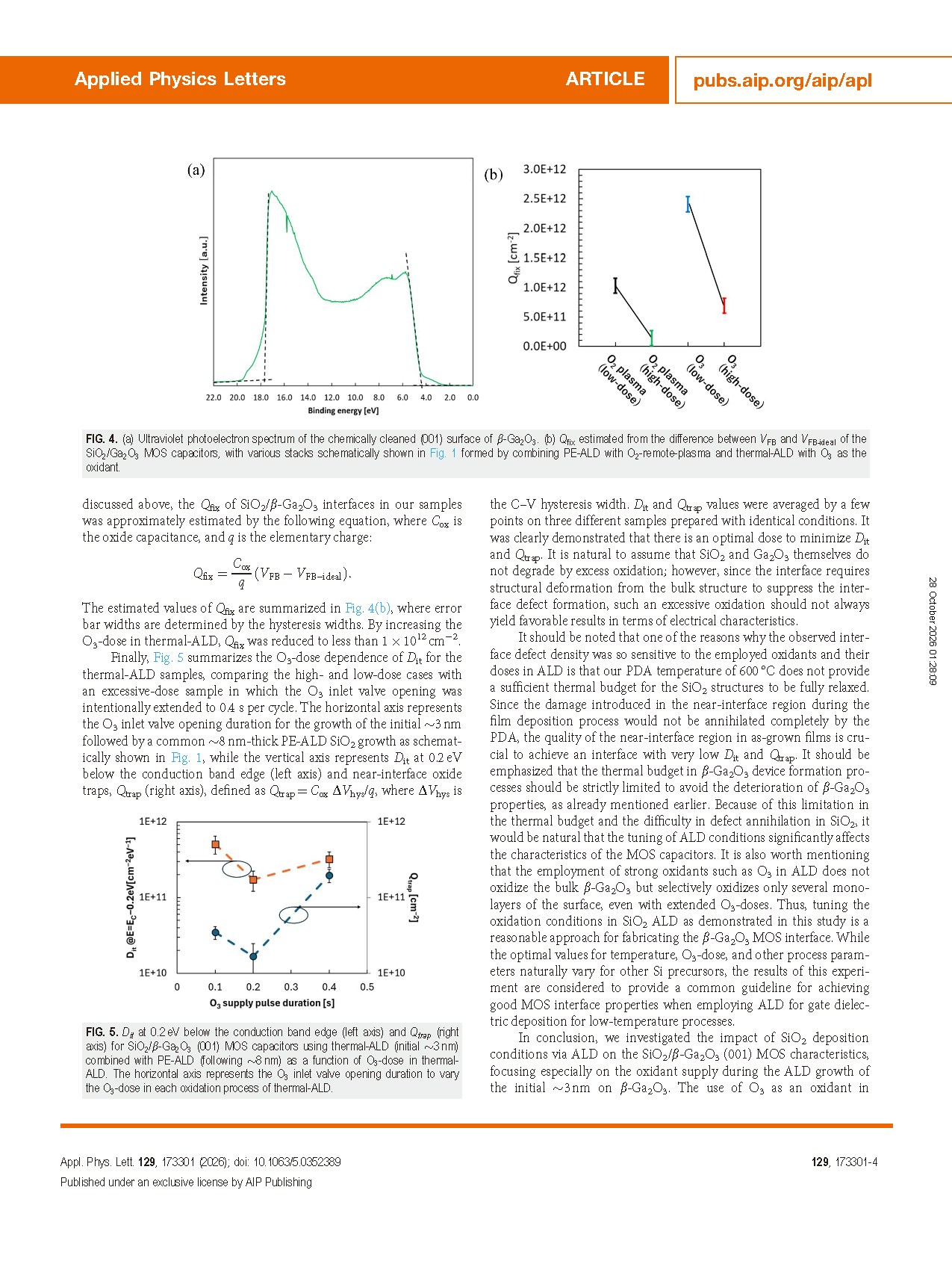
FIG. 4. (a) Ultraviolet photoelectron spectrum of the chemically cleaned (001) surface of β-Ga2O3. (b) Qfix estimated from the difference between VFB and VFB-ideal of the SiO2/Ga2O3 MOS capacitors, with various stacks schematically shown in Fig. 1 formed by combining PE-ALD with O2-remote-plasma and thermal-ALD with O3 as the oxidant.
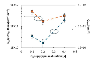
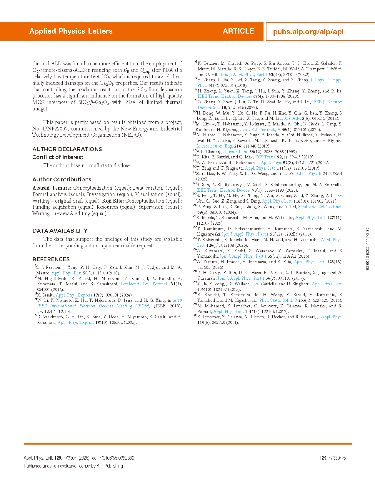
FIG. 5. Dit at 0.2 eV below the conduction band edge (left axis) and Qtrap (right axis) for SiO2/β-Ga2O3 (001) MOS capacitors using thermal-ALD (initial ~3 nm) combined with PE-ALD (following ~8 nm) as a function of O3-dose in thermal-ALD. The horizontal axis represents the O3 inlet valve opening duration to vary the O3-dose in each oxidation process of thermal-ALD.
DOI:
https://doi.org/10.1063/5.0352389
Instruction
Official Account

Cooperation
Top