
【International Papers】Silane-Mediated Expansion of Domains in Si-Doped κ-Ga₂O₃ Epitaxy and its Impact on the In-Plane Electronic Conduction
日期:2023-12-15阅读:867
Researchers from the University of Parma have published a dissertation titled " Silane-Mediated Expansion of Domains in Si-Doped κ-Ga2O3 Epitaxy and its Impact on the In-Plane Electronic Conduction " in Advanced Functional Materials.
Abstract
Unintentionally doped (001)-oriented orthorhombic κ-Ga2O3 epitaxial films on c-plane sapphire substrates are characterized by the presence of ≈ 10 nm wide columnar rotational domains that can severely inhibit in-plane electronic conduction. Comparing the in- and out-of-plane resistance on well-defined sample geometries, it is experimentally proved that the in-plane resistivity is at least ten times higher than the out-of-plane one. The introduction of silane during metal-organic vapor phase epitaxial growth not only allows for n-type Si extrinsic doping, but also results in the increase of more than one order of magnitude in the domain size (up to ≈ 300 nm) and mobility (highest µ ≈ 10 cm2V−1s−1, with corresponding lowest ρ ≈ 0.2 Ωcm). To qualitatively compare the mean domain dimension in κ-Ga2O3 epitaxial films, non-destructive experimental procedures are provided based on X-ray diffraction and Raman spectroscopy. The results of this study pave the way to significantly improved in-plane conduction in κ-Ga2O3 and its possible breakthrough in new generation electronics. The set of cross-linked experimental techniques and corresponding interpretation here proposed can apply to a wide range of material systems that suffer/benefit from domain-related functional properties.

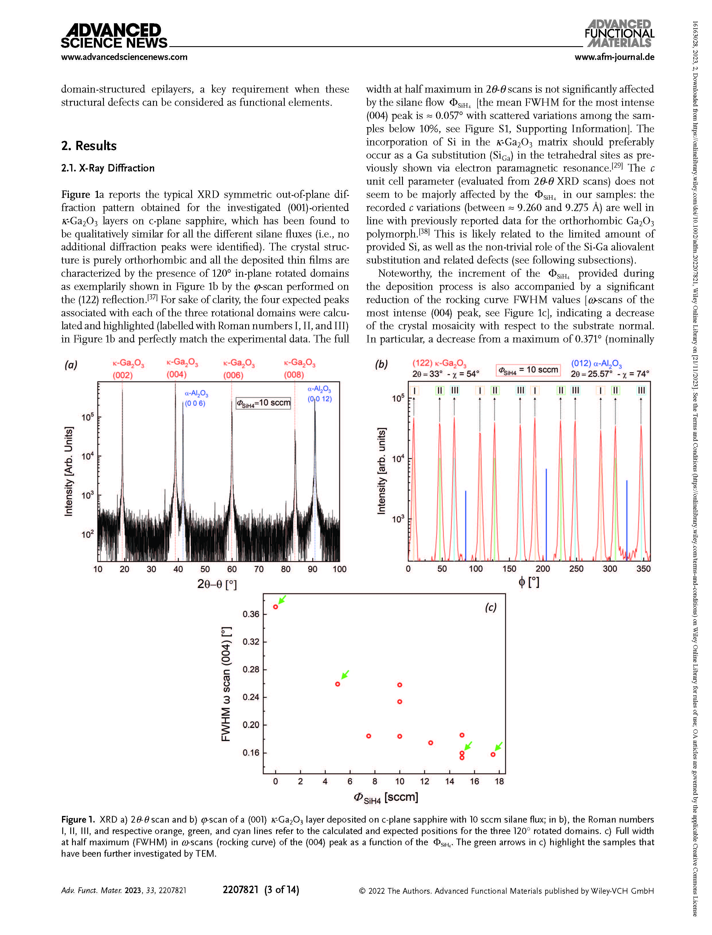
Figure 1 XRD a) 2θ-θ scan and b) φ-scan of a (001) κ-Ga2O3 layer deposited on c-plane sapphire with 10 sccm silane flux; in b), the Roman numbers I, II, III, and respective orange, green, and cyan lines refer to the calculated and expected positions for the three 120° rotated domains. c) Full width at half maximum (FWHM) in ω-scans (rocking curve) of the (004) peak as a function of the φSiH4. The green arrows in c) highlight the samples that have been further investigated by TEM.

Figure 2 Room temperature, a) electrical resistivity ρ, b) mobility µ, and c) charge carrier density n extracted from van der Pauw–Hall electrical measurements of Si-doped κ-Ga2O3 layers as a function of the φSiH4 provided during the deposition. The green arrows highlight the samples that have been further investigated by TEM.
Paper Link:https://doi.org/10.1002/adfm.202207821


