
【Conference Papers】IFWS 2023丨Report on the Fourth Generation Semiconductor Material Gallium Oxide Conference
日期:2024-01-12阅读:818
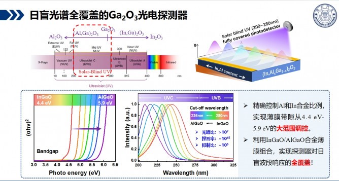
Xu Xiangyu, Xiamen University: Research on defect of Gallium Oxide, modulation of Alloy Engineering Electronic structures and development of Solar-blind photodetector

Semiconductor materials are the cornerstone of the information technology industry, and Gallium Oxide (Ga2O3) is a potential new ultra-wideband gap material, and Ga2O3 is an ideal choice for high-power, high-efficiency, UHV devices. It is also the preferred material for highly sensitive and highly responsive Solar-blind UV detector.
Recently, the 9th International Forum on Third Generation Semiconductors (IFWS) & The 20th China International Forum on Semiconductor Lighting (SSLCHINA) was held in Xiamen International Convention Center. During the session of "ultra-wide band gap Semiconductor Technology and Technology", Xu Xiangyu from Xiamen University brought the theme report of "Gallium Oxide defect Study, Alloy Engineering electronic Structure Modulation and Development of the Solar-blind photodetector", sharing the performance control research of high performance Ga2O3 photodetector. Photoelectric regulation and electronic structure of Al/In alloyed thin films, progress of vertical Schottky single crystal Ga2O3 photodetector.


The report pointed out that the high-performance Ga2O3 photodetector uses electronic packaging technology to achieve visual integration with the Internet of Things module, and completes the remote real-time monitoring of Gallium Oxide photodetectors on arc signals, Solar-blind LED and other light sources! Provide solutions for future industrial intelligent management. In terms of vertical Schottky single crystal Ga2O3 photodetector, the MSM structure detector has high responsiveness, but its weakness lies in its slow response speed. Strategy to improve device response speed: build built-in electric field, efficient separation, and accelerate drift. High quality single crystal ensures carrier mobility, and extremely low surface roughness ensures the lowest possible surface defect state. The Schottky contact is constructed by the large function metal to establish the internal electric field; Select ultra-thin and semi-transparent metal layer to ensure the effective light area and maximize the use of depletion layer for photoelectric conversion.
In this paper, a Solar-blind UV photodetector with high responsiveness and high detectivity was obtained by annealing the epitaxial film, and the sensitivity to the actual Solar-blind signal was realized. It is explained that the great improvement of device performance is influenced by defect caused by annealing and surface state change. By Al/In alloying of Ga2O3, a wide range of band gap regulation is achieved, and a UV photodetector capable of responding to all day blind band is prepared. The influence of alloying components on the band structure is explained. The semi-transparent Pt/Ga2O3 vertical structure Schottky photodiode was fabricated by high quality single crystal. The device has good photoelectric characteristics and successfully achieves the response speed without sustained photoconductance by adjusting the depth of interface depletion layer region.
High-throughput method to help screen and predict semiconductor interface structure: A case study of β-Ga2O3 /AlN interface

Semiconductors (IFWS) & the 20th China International Forum on Semiconductor Lighting (SSLCHINA) was held in Xiamen International Convention Center. During the "ultra-wide band gap Semiconductor Technology Branch", Feng Jiaren from Wuhan University shared a keynote report on "High-throughput Method Assisted Screening and prediction of semiconductor interface structure - taking β-Ga2O3 /AlN interface as an example".
Power electronic devices are widely used in all aspects of power transmission and transformation, and are widely used in major electricity-related fields. High-performance power electronic devices can reduce the loss in the process of power transmission and conversion, and help the "two-carbon" goal. Gallium Oxide is a variable semiconductor material that has six different crystalline phases, the most stable of which is the beta phase. Large sized single crystal substrates can be grown by melting of β-phase Gallium Oxide, which is very advantageous for the production of high-performance power devices, and its research has attracted much attention, but also faces challenges such as β-Ga2O3 material interface modeling.


Taking the β-Ga2O3 /AlN interface as an example, the report shared the research results of high-throughput methods to assist screening and predicting the interface structure of semiconductors, involving interface structure prediction, interface screening, interface batch generation, interface stability discussion, band alignment and other content. The high throughput search software package (IPG) for semiconductor interface structure was developed, and the Ga2O3 /AlN interface was taken as an example to verify the software function. From 70862440 configurations, the interface structure of several crystal faces was searched out. The analysis of electronic structure and band alignment was consistent with the experimental values. IPG software package is universal (metal/semiconductor interface, medium/semiconductor interface), which provides theoretical support for efficient design of electronic devices and accelerates material design.


