


Paper Sharing
【Member Papers】Nanjing University of Posts and Telecommunications (NUPT) Dr. Weihua Tang's Group Investigates the Method of Growing Sn:Ga₂O₃ by Mist-CVD
日期:2024-02-23阅读:982
Mist-chemical vapor deposition (mist-CVD) stands out as a widely employed technique for the growth of Ga2O3 thin films. This method boasts advantages such as vacuum-free operation, cost-effectiveness, and ease of operation. Notably, its compatibility with mainstream metal-organic chemical vapor deposition (MOCVD) technology, owing to the deposition of Ga2O3 through the reaction of organic gallium sources with oxygen, has garnered significant attention and extensive academic exploration. Despite existing reports on mist-CVD growth methods for Ga2O3 films, research on intentionally doped Ga2O3 films is relatively limited. Moreover, the majority of reported Ga2O3 films primarily focus on analog devices, with scarce studies on the fabrication of photodetectors.
This study successfully utilized mist-CVD technology to deposit a layer of tin-doped gallium oxide (Sn:Ga2O3) film on an α-Al2O3 substrate. The Mist-CVD configuration is a self-made system (as shown in Figure 1), comprising a tube furnace and a 2.4 MHz ultrasonic nebulizer. Utilizing air as the carrier gas, the nebulized solution of gallium acetylacetonate is transferred from the nebulizer to the substrate. The absorption spectrum of the film exhibited a wider bandgap compared to the common β-Ga2O3. X-ray diffraction (XRD) results indicated the coexistence of α-Ga2O3 and β-Ga2O3 phases in the film, while scanning electron microscopy (SEM) revealed the deposition of 125 nm of gallium oxide on the substrate within 30 minutes. (as shown in Figure 2) Employing a mechanical transfer method, we established a metal-semiconductor-metal (MSM) type photodetector by transferring electrodes onto the film. Under a bias voltage of -6 V, the photodetector demonstrated impressive performance, including a dark current as low as 10 pA and a photocurrent of 2.96 μA. The ratio of photocurrent to dark current reached an impressive 2.96×10⁵, with an external quantum efficiency of 245.79% and a photoresponsivity of 0.72 A/W. (as shown in Figure 3) In comparison to undoped gallium oxide films grown using the same technique (UID Ga2O3), photoconductivity and responsivity were enhanced by a factor of 103. This performance enhancement is attributed to the introduction of tin doping, which introduces deep-level donor impurity energy levels. Under illumination, carriers in the impurity energy levels are activated, leading to an increase in photocurrent. (as shown in Figure 4)
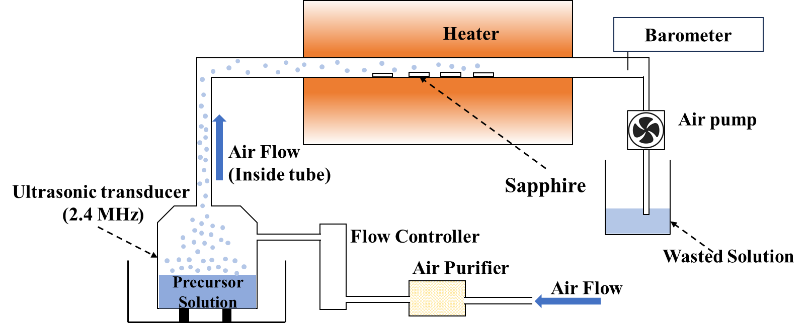
Figure 1 Schematics of home-made mist-CVD system.

Figure 2 UV–vis absorbance spectra of (a) Sn:Ga2O3and (b) UID Ga2O3 thin film. XRD pattern of (c) Sn:Ga2O3and (d) UID Ga2O3 thin film. (e) Surface and (f) cross section SEM photograph of the Sn: Ga2O3, (g) Surface and (h) cross section SEM photograph of the UID Ga2O3 thin film.

Figure 3 (a) Photoresponse spectrum of the device, (b) the I-V characteristics curves in the dark and under illumination of different light intensities of the device. (c) The functional relationship between the Iph and light intensity. (d) The relationship of R and EQE with light intensity.

Figure 4 The operating mechanism of (a) Sn: Ga2O3, (b) UID Ga2O3 MSM PD.(c) Conductance variation of PD. (d) Curve of photoconductive gain versus incident light intensity.
This research unveils the feasibility of employing the cost-effective mist-CVD growth method to fabricate Sn:Ga2O3 and its application in the preparation of deep ultraviolet photodetectors. Through tin doping, we successfully enhanced the device's detection capability for UV-C. Furthermore, we conducted an in-depth investigation into the mist-CVD growth of Sn:Ga2O3, exploring the physical mechanisms behind the enhancement of Ga2O3 photoconductivity due to Sn doping. This study provides new physical guidance for doping engineering. It contributes substantively to the advancement of deep ultraviolet photodetector technology, opening up new directions for future developments in the field of optoelectronic devices.


