Paper Sharing
【International Papers】Electronic states near surfaces and interfaces of β-Ga₂O₃ and κ-Ga₂O₃ epilayers investigated by surface photovoltage spectroscopy, photoconductivity and optical absorption
日期:2024-08-30阅读:906
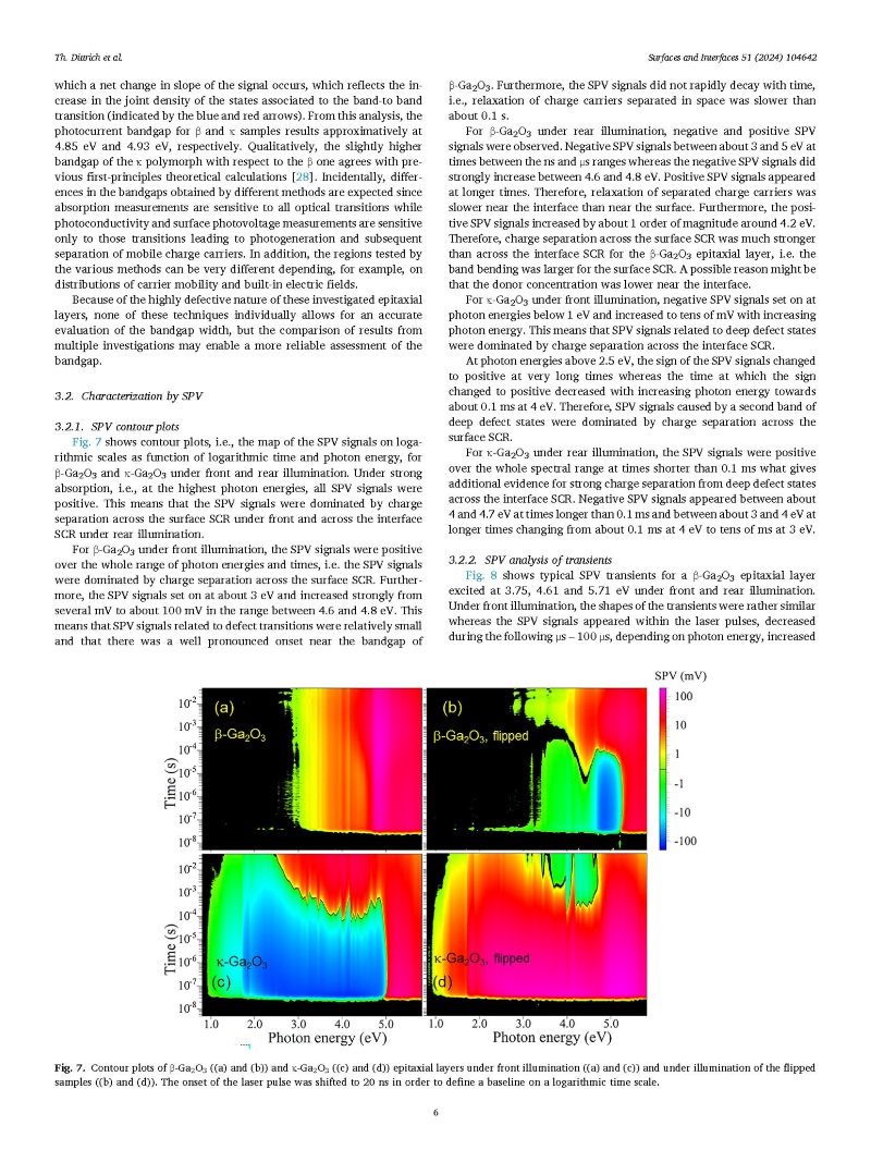
Researchers from the University of Parma have published a dissertation titled "Electronic states near surfaces and interfaces of β-Ga2O3 and κ-Ga2O3 epilayers investigated by surface photovoltage spectroscopy, photoconductivity and optical absorption" in Surfaces and Interfaces.
Abstract
Transient surface photovoltage (SPV) spectroscopy, optical absorption, and photoconductivity (PC) were applied to study electronic transitions in (-201) β-Ga2O3 and (001) κ-Ga2O3 epitaxial layers on c-plane sapphire substrates. SPV signals were distinguished for charge separation near the surface and near the layer/substrate interface. The bandgaps of β-Ga2O3 and κ-Ga2O3 epitaxial layers were found to be, respectively, about 4.75 and 4.79 eV from optical absorption measurements, about 4.8 and 4.9 eV from PC, and 4.65 and 4.9 (near the surface) from SPV measurements. Near the κ-Ga2O3 layer/substrate interface SPV instead gives a value of 4.75 eV, possibly related to the presence of an interlayer. Defect-related transitions with onset energies at about 4.5, 4.1, and 3.5 eV were observed along the whole β-Ga2O3 layer cross-section. In contrast, defects related to different transitions were differently distributed in κ-Ga2O3 epitaxial layers: transitions setting on at about 4.3 eV originate from defects uniformly distributed across the layer, while transitions starting at 2.4 eV and 1.7 eV were respectively connected with defects located near the surface or near the layer/substrate interface. The PC measurements at photo-excitation energy above the bandgap indicated that defect densities and recombination losses were much larger in κ-Ga2O3 than in β-Ga2O3.

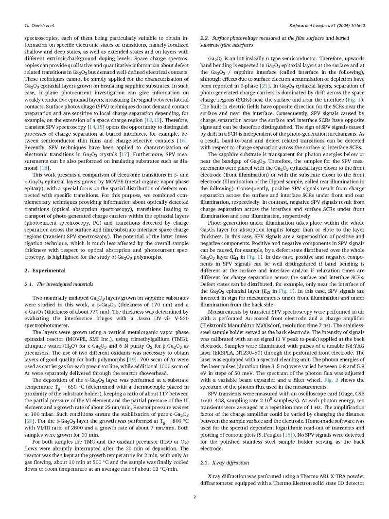
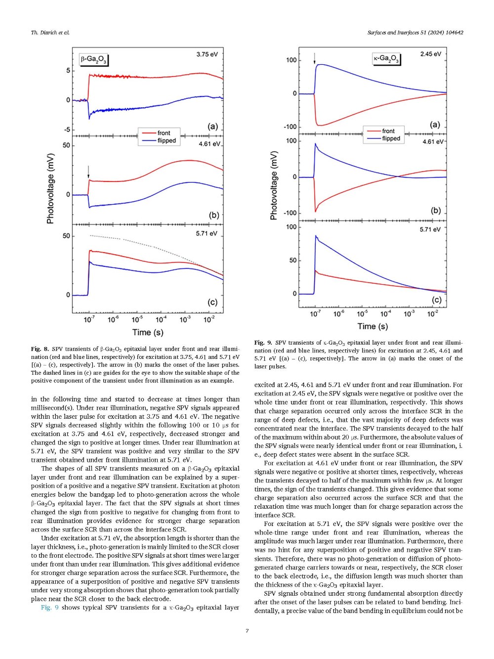
Fig. 1. Measurement arrangements (left) and schematic band diagrams (right) of a Ga2O3 epitaxial layer for SPV measurements under front illumination (a) and under illumination of the flipped sample (b). A, B, correspond to charge separation across the surface and interface SCRs under front illumination while C, D represent charge separation at the interface and surface SCRs under rear illumination. The corresponding SPV signals have positive (A and C) and negative (B and D) signs. EV, EC, Et1 and Et2 denote the valence and conduction band edges and defect states distributed over the whole layer and only near the interface, respectively.
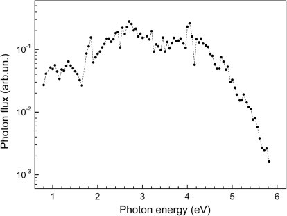
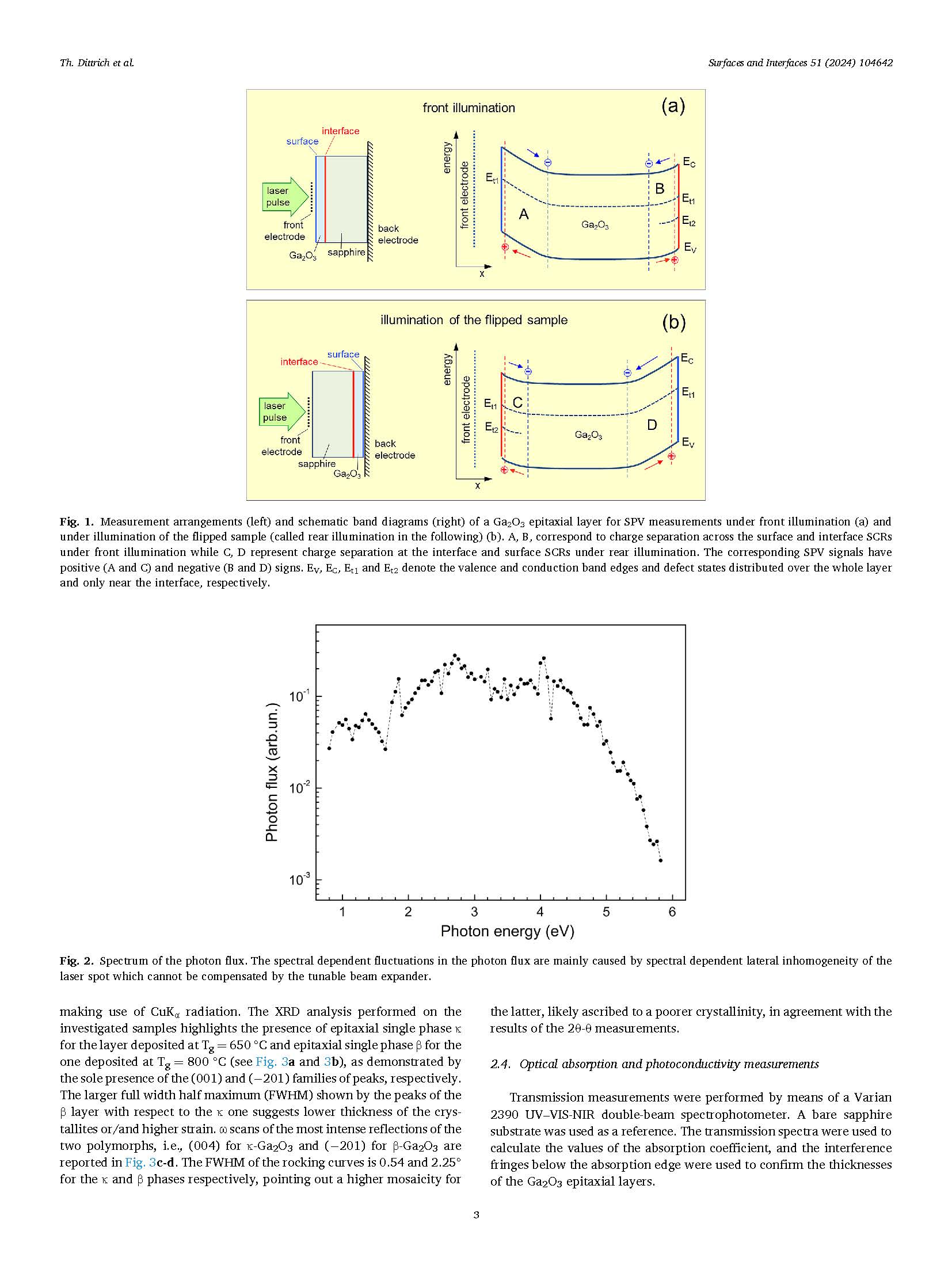
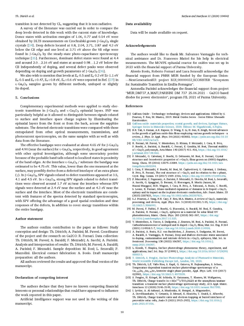
Fig. 2. Spectrum of the photon flux. The spectral dependent fluctuations in the photon flux are mainly caused by spectral dependent lateral inhomogeneity of the laser spot which cannot be compensated by the tunable beam expander.
DOI:doi.org/10.1016/j.surfin.2024.104642