News Trends
【World Express】Japan NEDO Layout Gallium Oxide to Help Semiconductor Industry Technological Breakthroughs
日期:2024-09-02阅读:1146
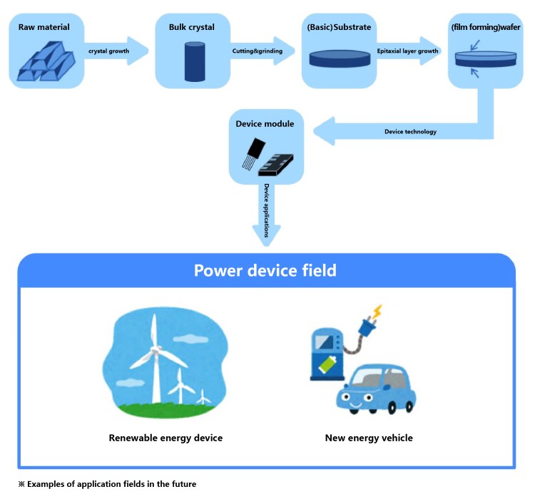
Japan’s New Energy and Industrial Technology Development Organization (NEDO) recently announced that it will focus on promoting technology development projects based on β-Gallium Oxide (β-Ga2O3) materials. The initiative aims to address the new challenges posed by the rapid adoption of renewable energy and electric vehicles, especially the urgent need for semiconductor devices with high output, high efficiency and tolerance to extreme environments.
As the demand for clean energy continues to increase worldwide, the limitations of traditional semiconductor materials such as Silicon (Si) and Silicon Carbide (SiC) in some demanding applications are becoming apparent. Compared to these materials, β-Ga2O3 is notable for its excellent dielectric breakdown strength. This characteristic makes β-Ga2O3 exhibit excellent performance in the medium and high voltage range, making it an ideal material for the development of high voltage power devices and modules.
In this project, NEDO plans to focus on the development of manufacturing technology for β-Ga2O3 wafers. The agency will study how the new material can be used in mass production to make it practical in terms of size, quality and cost. Through this technology development, it is expected that in the future, semiconductor devices can be produced that can adapt to harsh environments such as high temperatures, while having low loss and energy saving characteristics.
The successful development of this technology will not only have a profound impact on the semiconductor industry, but also play an important role in supporting the global green energy transition, improving the performance of electric vehicles and enhancing the reliability of energy infrastructure. In the future, with the further maturity of the technology, Gallium Oxide has a broad application prospect in the field of power electronics and power modules.
Executive Unit
Novel Crystal Technology (NCT)(Lead Enterprise)
Mitsubishi Electric
Japan Fine Ceramics Center (JFCC)
Project Duration (Expected)
2024 to 2028 (5 years)
Main Research and Development Content
□ Developed β-Ga2O3 crystal growth technology
□ Developed β-Ga2O3 epitaxy technology
□ Developed β-Ga2O3 defect detection technology
□ Developed β-Ga2O3 power devices
□ Developed β-Ga2O3 power module
Project Process