


Paper Sharing
【Domestic Papers】Professor Ma Xiaohua's Research Group From Xidian University Conducts Research on The β-Ga₂O₃ MOSFET Structure
日期:2024-09-13阅读:971
As a representative of ultra-wide band gap semiconductor materials, Gallium Oxide (Ga2O3) has an ultra-wide bandgap (4.9eV) and ultra-high critical breakdown field strength (8 MV/cm), and is considered as a promising semiconductor material for the preparation of the next generation of high-power, high-efficiency and low-power power electronic systems. In addition, it has been found that β-Ga2O3 also exhibits an electron saturation speed of up to 2×107 cm/s, and its Johnson's Figure of Merit (2844) is higher than that of SiC and GaN. Therefore, it has important application potential in the field of RF devices, and it is of great significance to explore and study Gallium Oxide based RF power devices.
However, in practical RF applications, the control circuit and power consumption need to be considered. Therefore, there is an urgent need for enhanced devices to simplify RF topological circuits and reduce static power consumption. Due to the deficiency of device design and process, the performance of Gallium Oxide based enhanced MOSFETs reported in the world is still poor. There are still many shortcomings in the RF performance of these enhanced devices, and the main limiting factor is the negative impact of the device process on the channel electron concentration and channel mobility. Therefore, it is very important to improve the device design and preparation process and effectively improve the channel mobility for the enhanced Ga2O3 base RF MOSFET.
Professor Ma Xiaohua's research group from Xidian University has innovatively proposed a quasi two-dimensional high mobility channel enhanced β-Ga2O3 MOSFET structure. Low damage etching technology is introduced to form a grooved gate structure, and the thickness of the heavily doped channel is reduced to a few nanometers, which reduces the vertical electron scattering and effectively improves the channel mobility. At the same time, the heavily doped material is used as the channel layer, which makes the device have small on-resistance and low ohmic contact resistance, so as to show excellent radio frequency performance. The research result is titled "Quasi 2D high mobility channel E-mode β-Ga2O3 MOSFET with Johnson FOM of 7.56 THz·V". The paper was published in the internationally renowned journal Applied Physics Letters. Wang Xizhen, PhD candidate of the class of 2021, is the first author of this paper, and Professor Ma Xiaohua, Professor Lu Xiaoli and Associate Professor He Yunlong are co-corresponding authors.
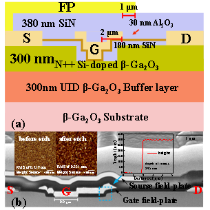
FIG. 1 Schematic diagram of device structure and SEM image
The study shows that the fabrication process of the device includes low-damage etching in the area under the gate, and the etching depth is 295 nm. The research team adopted a step-by-step etching method, using O2 plasma to repair the etching damage of the device. Oxygen plasma produces a large number of oxygen ions during the ionization process, and the oxygen vacancy existing in the Ga2O3 material can be supplemented by these oxygen ions. AFM images show that the change of surface roughness before and after etching is less than 0.15 nm, indicating that lower damage is introduced in the etching process, reducing the influence of ionized impurities scattering, thus ensuring the device has a high mobility.
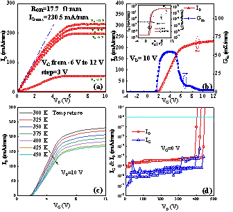
FIG. 2 Output characteristics, transfer characteristics, thermal stability and breakdown characteristics of the device
According to the calculation of CV curve, the device field mobility is 147.5cm2 /(V·s), and the excellent device mobility makes it have good RF characteristics, and the peak transconductance of the device is as high as 54.2 m S/mm. The excellent mobility is one of the reasons for the high transconductance, which is also in line with the transfer characteristics of the device.
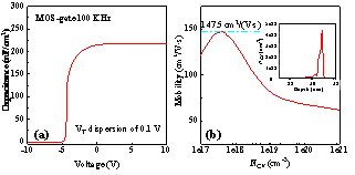
FIG. 3 CV curve of the device and the variation of device mobility with carrier concentration
In addition, the mobility and RF characteristics of devices with different channel thicknesses are also shown from the simulation results. The devices with smaller channel thicknesses have better performance, which is consistent with the experimental results, and provides theoretical support for the experiment. Especially when the channel thickness in the region beneath the gate is reduced to the order of nanometers, the electron scattering in the vertical direction can be ignored to a certain extent, thus achieving a quasi-two-dimensional channel similar to 2DEG, effectively improving the channel mobility of the device and improving the RF characteristics of the device.
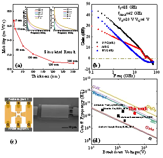
FIG. 4 Mobility simulation results, device small signal characteristics, de-embedding structure and Johnson's Figure of Merit diagram
In terms of small signal characteristics of the device, fT and fMAX of the device are 18 GHz and 42 GHz respectively. The Johnson's Figure of Merit fT×VBK is 7.56 THz·V, which reaches the highest value of Gallium Oxide enhanced MOSFET devices known in the world. This result lays a foundation for the application of β-Ga2O3 based MOSFET in future RF power electronics devices.
The research was supported by the National Key Laboratory of Wide Band Gap Semiconductor Devices and Integration Technology Open Project, the Fundamental Research Funds for the Central Universities, and the National Innovation Center for Radiation Application.
