


Paper Sharing
【Domestic Papers】Ultrathin Sn-doped Ga₂O₃ for power field-effect transistors: Si-compatible 4-inch array with high-k gate dielectric
日期:2024-09-20阅读:891
Researchers from the Beijing Institute of Technology have published a dissertation titled "Ultrathin Sn-doped Ga2O3 for power field-effect transistors: Si-compatible 4-inch array with high-k gate dielectric " in Science Bulletin.
Gallium oxide (Ga2O3), a novel ultrawide-bandgap (UWBG) semiconductor, has attracted considerable attention owing to its large bandgap of up to 4.9 eV, a high breakdown electric field of 8 MV/cm, and a high Baliga’s figure of merit exceeding 3000. These remarkable properties strongly support its potential applications in power electronics, extreme environmentresistance devices, and solar-blind detectors. Despite recent advancements in Ga2O3 film growth for device fabrication, the reported methods often entail high temperatures of 1000 C, complex processes, and the need for homogeneous substrates, which inevitably escalates production costs, limiting mass production feasibility. In contrast, physical vapor deposition (PVD) methods such as magnetron sputtering have successfully shown advantages for oxide semiconductors and associated devices. These benefits include compatibility with silicon, low cost, low temperature, flexible doping modulation, large-area growth, and rapid production. However, the utilization of PVD methods for UWBG Ga2O3 and its application in power devices has been neglected to some extent.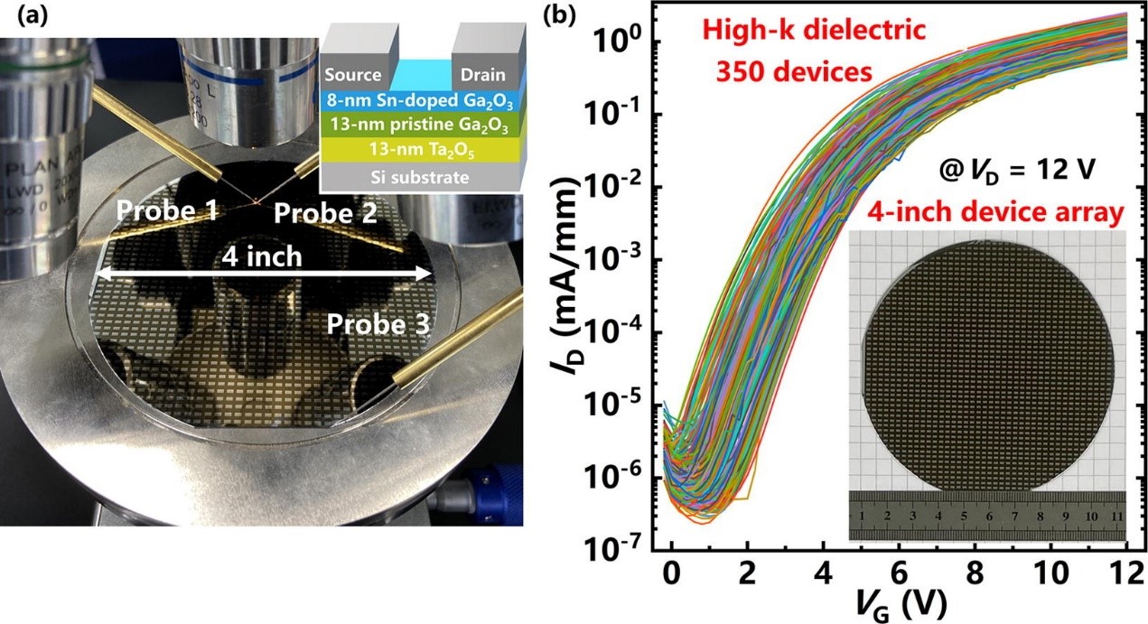
DOI:https://doi.org/10.1016/j.scib.2024.04.059
